PRESENTED BY:- SAGAR NETAM
INTRODUCTION
 There are three types of configurations in which
Transistor operation is carried out namely CB,CE,CC.
 CC :In this circuit the base terminal of the transistor
serves as the input, the emitter is the output, and the
collector is common to both
 Signal input between base and common collector.
 Signal output between emitter and common collector.
 The CC circuit is also known as an emitter follower
since the output voltage at the emitter follows the
input voltage at the base.
 It has voltage gain slightly less than unity.
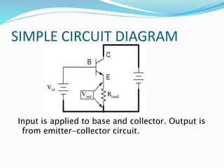
SIMPLE CIRCUIT DIAGRAM
Input is applied to base and collector. Output is
from emitter-collector circuit.
WORKING :INPUT CHARACTERISTICS
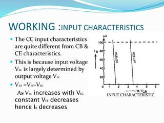
 The CC input characteristics
are quite different from CB &
CE characteristics.
 This is because input voltage
VBC is largely determined by
output voltage VEC
 VEB =VEC-VBC
As VBC increases with VEC
constant VEB decreases
hence IB decreases
INPUT CHARACTERISTIC
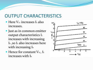
OUTPUT CHARACTERISTICS
 Here VCE increases IE also
increases.
 Just as in common emitter
output characteristics IC
increases with increasing
IB ,so IE also increases here
with increasing IB
 Hence for constant VEC, IE
increases with IB
APPLICATION
 It is useful as an impedance matching device since its
input impedance is much higher than its output
impedance. It is also termed a “buffer" for this reason
and is used in digital circuits with basic gates.
 When the voltage divider used but it is a poor voltage
source because it is so strongly affected by the value of
the load resistor. The same voltage divider with the
transistor buffer will supply power to keep the voltage
constant over its range of operation.
 It is also used for cascade amplifier.
Common collector

Common collector

  • 1.
  • 2.
    INTRODUCTION  There arethree types of configurations in which Transistor operation is carried out namely CB,CE,CC.  CC :In this circuit the base terminal of the transistor serves as the input, the emitter is the output, and the collector is common to both  Signal input between base and common collector.  Signal output between emitter and common collector.  The CC circuit is also known as an emitter follower since the output voltage at the emitter follows the input voltage at the base.  It has voltage gain slightly less than unity.
  • 3.
    SIMPLE CIRCUIT DIAGRAM Inputis applied to base and collector. Output is from emitter-collector circuit.
  • 4.
    WORKING :INPUT CHARACTERISTICS The CC input characteristics are quite different from CB & CE characteristics.  This is because input voltage VBC is largely determined by output voltage VEC  VEB =VEC-VBC As VBC increases with VEC constant VEB decreases hence IB decreases INPUT CHARACTERISTIC
  • 5.
    OUTPUT CHARACTERISTICS  HereVCE increases IE also increases.  Just as in common emitter output characteristics IC increases with increasing IB ,so IE also increases here with increasing IB  Hence for constant VEC, IE increases with IB
  • 6.
    APPLICATION  It isuseful as an impedance matching device since its input impedance is much higher than its output impedance. It is also termed a “buffer" for this reason and is used in digital circuits with basic gates.  When the voltage divider used but it is a poor voltage source because it is so strongly affected by the value of the load resistor. The same voltage divider with the transistor buffer will supply power to keep the voltage constant over its range of operation.  It is also used for cascade amplifier.