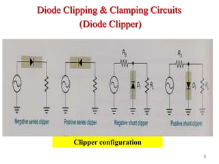
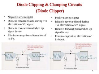
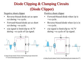
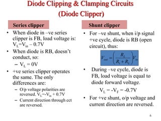
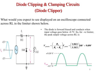
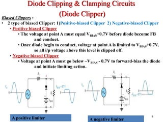
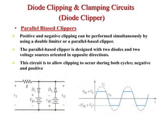
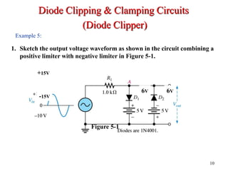
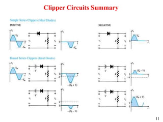
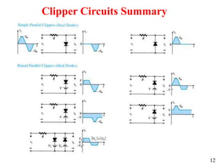
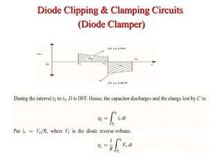
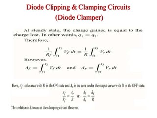
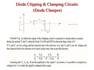
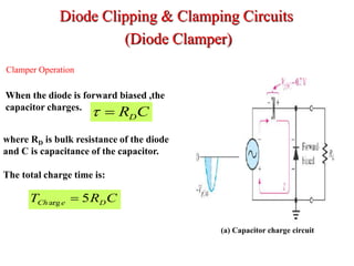
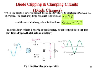
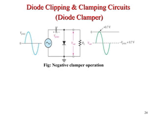
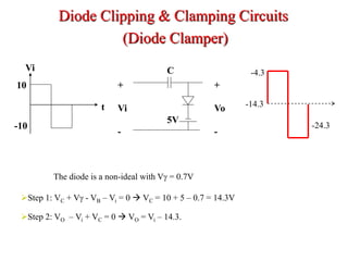
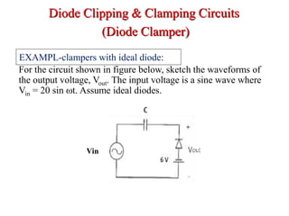
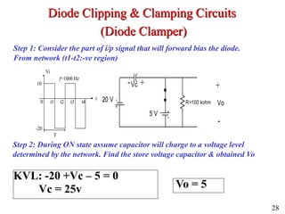
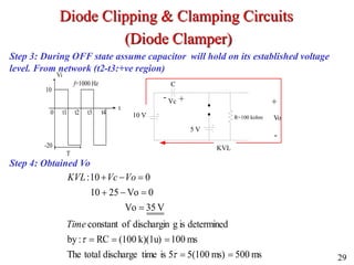
Clippers and Clampers
• Diode limiters/clippers – that limits/clips the portion of signal
voltage above or below certain level.
• Limiting circuits limit the positive or negative amount of an
input voltage to a specific value.
• 4 basic clipper configuration:
– Negative series clipper diode is in series with its load
– Positive series clipper
– Negative shunt clipper diode is in parallel with its load
– Positive shunt clipper
2
Diode Clipping & Clamping Circuits
(Diode Clipper)
3
Clipper configuration
Diode Clipping & Clamping Circuits
(Diode Clipper)
• Positive series clipper
• Diode is reverse-biased during
+ve alternation of i/p signal.
• Diode is forward-biased when i/p
signal is –ve.
• Eliminates positive alternation of
its input.
4
• Negative series clipper
• Diode is forward-biased during +ve
alternation of i/p signal.
• Diode is reverse-biased when i/p
signal is –ve.
• Eliminates negatives alternation of
its i/p.
Diode Clipping & Clamping Circuits
(Diode Clipper)
Negative shunt clipper
• Reverse-biased diode act as open
cct during +ve cycle.
• Forward-biased diode act as short
cct during –ve cycle.
• o/p signal is limit/clip to -0.7V
during –ve cycle of i/p signal.
Positive shunt clipper
• Forward-biased diode when i/p is
+ve cycle.
• Reverse-biased diode when i/p is in
–ve cycle.
• o/p signal is limit/clip to +0.7V
during +ve cycle of i/p signal.
5
Diode Clipping & Clamping Circuits
(Diode Clipper)
Series clipper
• When diode in –ve series
clipper is FB, load voltage is:
VL=Vin – 0.7V
• When diode is RB, doesn’t
conduct, so:
– VL = 0V
• +ve series clipper operates
the same. The only
differences are:
– O/p voltage polarities are
reversed. VL=-Vin + 0.7V
– Current direction through cct
are reversed.
Shunt clipper
• For –ve shunt, when i/p signal
+ve cycle, diode is RB (open
circuit), thus:
• During –ve cycle, diode is
FB, load voltage is equal to
diode forward voltage.
VL = -VF = -0.7V
• For +ve shunt, o/p voltage and
current direction are reversed.
6
in
L
L
out V
R
R
R
V 









1
Diode Clipping & Clamping Circuits
(Diode Clipper)
7
What would you expect to see displayed on an oscilloscope connected
across RL in the limiter shown below.
• The diode is forward biased and conducts when
input voltage goes below -0.7V. So, for –ve limiter,
the peak output voltage across RL is:
V
V
k
k
V
R
R
R
V in
p
L
L
out
p 09
.
9
10
1
.
1
0
.
1
)
(
1
)
( 



















Diode Clipping & Clamping Circuits
(Diode Clipper)
8
Biased Clippers :
• 2 type of biased Clipper: 1)Positive-biased Clipper 2) Negative-biased Clipper
• Positive biased Clipper
• The voltage at point A must equal VBIAS+0.7V before diode become FB
and conduct.
• Once diode begin to conduct, voltage at point A is limited to VBIAS+0.7V,
so all i/p voltage above this level is clipped off.
• Negative biased Clipper
• Voltage at point A must go below –VBIAS - 0.7V to forward-bias the diode
and initiate limiting action.
A positive limiter A negative limiter
Diode Clipping & Clamping Circuits
(Diode Clipper)
• Parallel Biased Clippers
 Positive and negative clipping can be performed simultaneously by
using a double limiter or a parallel-based clipper.
 The parallel-based clipper is designed with two diodes and two
voltage sources oriented in opposite directions.
 This circuit is to allow clipping to occur during both cycles; negative
and positive
Diode Clipping & Clamping Circuits
(Diode Clipper)
10
Example 5:
1. Sketch the output voltage waveform as shown in the circuit combining a
positive limiter with negative limiter in Figure 5-1.
Figure 5-1
+15V
-15V
6V 6V
Diode Clipping & Clamping Circuits
(Diode Clipper)
11
Clipper Circuits Summary
12
• Half-wave rectifier
– Circuit alters the shape of ac signal and change it to pulsating dc.
• Transient protection circuit
– Transient  abrupt current or voltage spike in short duration.
– Many digital circuits have i/p that cannot tolerate voltage fall outside a
specified range which can cause serious damage. A clipper can be used
to protect these circuits.
• AM detector
– Eliminate –ve portion of i/p waveform, so capacitor charges and
discharges at rate of peak i/p variations. This provides a signal at load
that is a reproduction of i/p signal.
13
Diode Clipping & Clamping Circuits
(Diode Clipper)
•Shift a waveform either above or below a given reference voltage
without distorting the waveform.
•Clamp a signal to a different dc level.
• known as DC restorers.
•used in TV Receivers as a DC Restorer.
• The network consists of:
a) Capacitor
b) Diode
c) Resistive element
d) Independent dc supply (option)
•T= RC is large enough to ensure that the voltage across the capacitor does not
discharge significantly during the interval the diode is nonconducting.
• Our analysis basis that all capacitor is fully charge and discharge in 5 time constant.
14
Diode Clipping & Clamping Circuits
(Diode Clamper)
Types:
2) Negative Clamper
1) Positive Clamper
Diode Clipping & Clamping Circuits
(Diode Clamper)
Diode Clipping & Clamping Circuits
(Diode Clamper)
Clamping Circuit Theorem:
• This theorem enables us to calculate the voltage
level to which the output is clamped by
considering the areas above and below the
reference level, when the values of Rf and R are
known.
• The clamping circuit theorem states that under
steady-state conditions, for any input waveform,
the ratio of the area under the output voltage
curve in the forward direction to that in the
reverse direction is equal to the ratio Rf /R.
• To prove the clamping circuit theorem, consider a typical
steady-state output for the clamping circuit, represented below:
Diode Clipping & Clamping Circuits
(Diode Clamper)
Diode Clipping & Clamping Circuits
(Diode Clamper)
Diode Clipping & Clamping Circuits
(Diode Clamper)
Diode Clipping & Clamping Circuits
(Diode Clamper)
When the diode is forward biased ,the
capacitor charges.
C
RD


where RD is bulk resistance of the diode
and C is capacitance of the capacitor.
The total charge time is:
C
R
T D
e
Ch 5
arg 
(a) Capacitor charge circuit
Clamper Operation
Diode Clipping & Clamping Circuits
(Diode Clamper)
22
When the diode is reverse biased, the capacitor starts to discharge through RL.
Therefore, the discharge time constant is found as: C
RL


C
R
T L
e
Disch 5
arg 
and the total discharge time is found as:
The capacitor retains a charge approximately equal to the input peak less
the diode drop so that it acts as a battery.
Fig.: Positive clamper operation
Reverse-
biased
Diode Clipping & Clamping Circuits
(Diode Clamper)
23
Operation of clamper
+ ve region
+
R Vo
-
+
-
Vi
C
• 0 - T/2: Diode is ON state
(short-ckt equivalent)
• Assume RC time is small
and capacitor charge to V
volts very quickly
• Vo=0 V (ideal diode)
- ve region • T/2- T: Diode is OFF state
(open-ckt equivalent)
• Both for the stored voltage
across capacitor and applied
signal current through
cathode to anode
• KVL: - V- V- Vo = 0 and
Vo = -2V
+
R Vo
-
+
-
V
C
Vo
-
+
V
Vi
t
0 T/2 T
V
-V
Total swing
o/p signal =
the total swing
i/p signal
+
R Vo
-
+
-
Vi
Vi
t
0 T/2 T
V
-V
24
Fig: Negative clamper operation
Diode Clipping & Clamping Circuits
(Diode Clamper)
 STEP 1: Knowing what value that the capacitor is charged to. And
from the polarity of the diode, we know that it is charged during
positive cycle. Using KVL,
 VC + VB – VS = 0  VC = VM – VB
 STEP 2: When the diode is reversed biased and VC is already a
constant value
 VO – VS + VC = 0  VO = VS – VC.
● A clamping circuit that includes an independent voltage source VB.
Peak value VM
Diode Clipping & Clamping Circuits
(Diode Clamper)
C
+
Vo
-
5V
+
Vi
-
Vi
t
-10
10
The diode is a non-ideal with V = 0.7V
Step 1: VC + V - VB – Vi = 0  VC = 10 + 5 – 0.7 = 14.3V
Step 2: VO – Vi + VC = 0  VO = Vi – 14.3.
-4.3
-24.3
-14.3
Diode Clipping & Clamping Circuits
(Diode Clamper)
EXAMPL-clampers with ideal diode:
For the circuit shown in figure below, sketch the waveforms of
the output voltage, Vout. The input voltage is a sine wave where
Vin = 20 sin t. Assume ideal diodes.
Vin
Diode Clipping & Clamping Circuits
(Diode Clamper)
28
Step 1: Consider the part of i/p signal that will forward bias the diode.
From network (t1-t2:-ve region)
+
R=100 kohm Vo
-
+
-
20 V
Vc
5 V
Step 2: During ON state assume capacitor will charge to a voltage level
determined by the network. Find the store voltage capacitor & obtained Vo
KVL: -20 +Vc – 5 = 0
Vc = 25v Vo = 5
Vi
-20
10
T
0 t1 t2 t3 t4
t
f=1000 Hz
Diode Clipping & Clamping Circuits
(Diode Clamper)
29
Step 3: During OFF state assume capacitor will hold on its established voltage
level. From network (t2-t3:+ve region)
+
R=100 kohm Vo
-
+
-
10 V
C
Vc
5 V
KVL
Step 4: Obtained Vo
ms
500
ms)
5(100
5
is
time
discharge
total
The
ms
100
k)(1u)
(100
RC
:
by
determined
is
g
dischargin
of
constant
V
35
Vo
0
Vo
25
10
0
10
:














Time
Vo
Vc
KVL
Vi
-20
10
T
0 t1 t2 t3 t4
t
f=1000 Hz
Diode Clipping & Clamping Circuits
(Diode Clamper)
Step 5: Checking!!! total swing o/p signal = total swing i/p signal From
network (t2-t3: +ve region)
Vo
35
0 t1 t2 t3 t4 t
5
Vi
-20
10
T
0 t1 t2 t3 t4
t
f=1000 Hz
30
Diode Clipping & Clamping Circuits
(Diode Clamper)
Summary of Clamper Circuits
31

Clippers_and_Clampers.pptx

  • 1.
  • 2.
    • Diode limiters/clippers– that limits/clips the portion of signal voltage above or below certain level. • Limiting circuits limit the positive or negative amount of an input voltage to a specific value. • 4 basic clipper configuration: – Negative series clipper diode is in series with its load – Positive series clipper – Negative shunt clipper diode is in parallel with its load – Positive shunt clipper 2 Diode Clipping & Clamping Circuits (Diode Clipper)
  • 3.
    3 Clipper configuration Diode Clipping& Clamping Circuits (Diode Clipper)
  • 4.
    • Positive seriesclipper • Diode is reverse-biased during +ve alternation of i/p signal. • Diode is forward-biased when i/p signal is –ve. • Eliminates positive alternation of its input. 4 • Negative series clipper • Diode is forward-biased during +ve alternation of i/p signal. • Diode is reverse-biased when i/p signal is –ve. • Eliminates negatives alternation of its i/p. Diode Clipping & Clamping Circuits (Diode Clipper)
  • 5.
    Negative shunt clipper •Reverse-biased diode act as open cct during +ve cycle. • Forward-biased diode act as short cct during –ve cycle. • o/p signal is limit/clip to -0.7V during –ve cycle of i/p signal. Positive shunt clipper • Forward-biased diode when i/p is +ve cycle. • Reverse-biased diode when i/p is in –ve cycle. • o/p signal is limit/clip to +0.7V during +ve cycle of i/p signal. 5 Diode Clipping & Clamping Circuits (Diode Clipper)
  • 6.
    Series clipper • Whendiode in –ve series clipper is FB, load voltage is: VL=Vin – 0.7V • When diode is RB, doesn’t conduct, so: – VL = 0V • +ve series clipper operates the same. The only differences are: – O/p voltage polarities are reversed. VL=-Vin + 0.7V – Current direction through cct are reversed. Shunt clipper • For –ve shunt, when i/p signal +ve cycle, diode is RB (open circuit), thus: • During –ve cycle, diode is FB, load voltage is equal to diode forward voltage. VL = -VF = -0.7V • For +ve shunt, o/p voltage and current direction are reversed. 6 in L L out V R R R V           1 Diode Clipping & Clamping Circuits (Diode Clipper)
  • 7.
    7 What would youexpect to see displayed on an oscilloscope connected across RL in the limiter shown below. • The diode is forward biased and conducts when input voltage goes below -0.7V. So, for –ve limiter, the peak output voltage across RL is: V V k k V R R R V in p L L out p 09 . 9 10 1 . 1 0 . 1 ) ( 1 ) (                     Diode Clipping & Clamping Circuits (Diode Clipper)
  • 8.
    8 Biased Clippers : •2 type of biased Clipper: 1)Positive-biased Clipper 2) Negative-biased Clipper • Positive biased Clipper • The voltage at point A must equal VBIAS+0.7V before diode become FB and conduct. • Once diode begin to conduct, voltage at point A is limited to VBIAS+0.7V, so all i/p voltage above this level is clipped off. • Negative biased Clipper • Voltage at point A must go below –VBIAS - 0.7V to forward-bias the diode and initiate limiting action. A positive limiter A negative limiter Diode Clipping & Clamping Circuits (Diode Clipper)
  • 9.
    • Parallel BiasedClippers  Positive and negative clipping can be performed simultaneously by using a double limiter or a parallel-based clipper.  The parallel-based clipper is designed with two diodes and two voltage sources oriented in opposite directions.  This circuit is to allow clipping to occur during both cycles; negative and positive Diode Clipping & Clamping Circuits (Diode Clipper)
  • 10.
    10 Example 5: 1. Sketchthe output voltage waveform as shown in the circuit combining a positive limiter with negative limiter in Figure 5-1. Figure 5-1 +15V -15V 6V 6V Diode Clipping & Clamping Circuits (Diode Clipper)
  • 11.
  • 12.
  • 13.
    • Half-wave rectifier –Circuit alters the shape of ac signal and change it to pulsating dc. • Transient protection circuit – Transient  abrupt current or voltage spike in short duration. – Many digital circuits have i/p that cannot tolerate voltage fall outside a specified range which can cause serious damage. A clipper can be used to protect these circuits. • AM detector – Eliminate –ve portion of i/p waveform, so capacitor charges and discharges at rate of peak i/p variations. This provides a signal at load that is a reproduction of i/p signal. 13 Diode Clipping & Clamping Circuits (Diode Clipper)
  • 14.
    •Shift a waveformeither above or below a given reference voltage without distorting the waveform. •Clamp a signal to a different dc level. • known as DC restorers. •used in TV Receivers as a DC Restorer. • The network consists of: a) Capacitor b) Diode c) Resistive element d) Independent dc supply (option) •T= RC is large enough to ensure that the voltage across the capacitor does not discharge significantly during the interval the diode is nonconducting. • Our analysis basis that all capacitor is fully charge and discharge in 5 time constant. 14 Diode Clipping & Clamping Circuits (Diode Clamper)
  • 15.
    Types: 2) Negative Clamper 1)Positive Clamper Diode Clipping & Clamping Circuits (Diode Clamper)
  • 16.
    Diode Clipping &Clamping Circuits (Diode Clamper) Clamping Circuit Theorem: • This theorem enables us to calculate the voltage level to which the output is clamped by considering the areas above and below the reference level, when the values of Rf and R are known. • The clamping circuit theorem states that under steady-state conditions, for any input waveform, the ratio of the area under the output voltage curve in the forward direction to that in the reverse direction is equal to the ratio Rf /R.
  • 17.
    • To provethe clamping circuit theorem, consider a typical steady-state output for the clamping circuit, represented below: Diode Clipping & Clamping Circuits (Diode Clamper)
  • 18.
    Diode Clipping &Clamping Circuits (Diode Clamper)
  • 19.
    Diode Clipping &Clamping Circuits (Diode Clamper)
  • 20.
    Diode Clipping &Clamping Circuits (Diode Clamper)
  • 21.
    When the diodeis forward biased ,the capacitor charges. C RD   where RD is bulk resistance of the diode and C is capacitance of the capacitor. The total charge time is: C R T D e Ch 5 arg  (a) Capacitor charge circuit Clamper Operation Diode Clipping & Clamping Circuits (Diode Clamper)
  • 22.
    22 When the diodeis reverse biased, the capacitor starts to discharge through RL. Therefore, the discharge time constant is found as: C RL   C R T L e Disch 5 arg  and the total discharge time is found as: The capacitor retains a charge approximately equal to the input peak less the diode drop so that it acts as a battery. Fig.: Positive clamper operation Reverse- biased Diode Clipping & Clamping Circuits (Diode Clamper)
  • 23.
    23 Operation of clamper +ve region + R Vo - + - Vi C • 0 - T/2: Diode is ON state (short-ckt equivalent) • Assume RC time is small and capacitor charge to V volts very quickly • Vo=0 V (ideal diode) - ve region • T/2- T: Diode is OFF state (open-ckt equivalent) • Both for the stored voltage across capacitor and applied signal current through cathode to anode • KVL: - V- V- Vo = 0 and Vo = -2V + R Vo - + - V C Vo - + V Vi t 0 T/2 T V -V Total swing o/p signal = the total swing i/p signal + R Vo - + - Vi Vi t 0 T/2 T V -V
  • 24.
    24 Fig: Negative clamperoperation Diode Clipping & Clamping Circuits (Diode Clamper)
  • 25.
     STEP 1:Knowing what value that the capacitor is charged to. And from the polarity of the diode, we know that it is charged during positive cycle. Using KVL,  VC + VB – VS = 0  VC = VM – VB  STEP 2: When the diode is reversed biased and VC is already a constant value  VO – VS + VC = 0  VO = VS – VC. ● A clamping circuit that includes an independent voltage source VB. Peak value VM Diode Clipping & Clamping Circuits (Diode Clamper)
  • 26.
    C + Vo - 5V + Vi - Vi t -10 10 The diode isa non-ideal with V = 0.7V Step 1: VC + V - VB – Vi = 0  VC = 10 + 5 – 0.7 = 14.3V Step 2: VO – Vi + VC = 0  VO = Vi – 14.3. -4.3 -24.3 -14.3 Diode Clipping & Clamping Circuits (Diode Clamper)
  • 27.
    EXAMPL-clampers with idealdiode: For the circuit shown in figure below, sketch the waveforms of the output voltage, Vout. The input voltage is a sine wave where Vin = 20 sin t. Assume ideal diodes. Vin Diode Clipping & Clamping Circuits (Diode Clamper)
  • 28.
    28 Step 1: Considerthe part of i/p signal that will forward bias the diode. From network (t1-t2:-ve region) + R=100 kohm Vo - + - 20 V Vc 5 V Step 2: During ON state assume capacitor will charge to a voltage level determined by the network. Find the store voltage capacitor & obtained Vo KVL: -20 +Vc – 5 = 0 Vc = 25v Vo = 5 Vi -20 10 T 0 t1 t2 t3 t4 t f=1000 Hz Diode Clipping & Clamping Circuits (Diode Clamper)
  • 29.
    29 Step 3: DuringOFF state assume capacitor will hold on its established voltage level. From network (t2-t3:+ve region) + R=100 kohm Vo - + - 10 V C Vc 5 V KVL Step 4: Obtained Vo ms 500 ms) 5(100 5 is time discharge total The ms 100 k)(1u) (100 RC : by determined is g dischargin of constant V 35 Vo 0 Vo 25 10 0 10 :               Time Vo Vc KVL Vi -20 10 T 0 t1 t2 t3 t4 t f=1000 Hz Diode Clipping & Clamping Circuits (Diode Clamper)
  • 30.
    Step 5: Checking!!!total swing o/p signal = total swing i/p signal From network (t2-t3: +ve region) Vo 35 0 t1 t2 t3 t4 t 5 Vi -20 10 T 0 t1 t2 t3 t4 t f=1000 Hz 30 Diode Clipping & Clamping Circuits (Diode Clamper)
  • 31.
    Summary of ClamperCircuits 31