This document contains 13 solved problems related to rectifier circuits using diodes. The problems calculate various electrical characteristics of half-wave, full-wave, and bridge rectifier circuits, including DC and AC voltages and currents, power delivered to loads, ripple factor, transformer specifications, and diode voltage ratings. Example calculations are shown for circuits using a single diode, full-wave rectifiers, and full-wave rectifiers with LC filter components.
These slides provide an elementary description of Power Electronics and its application domains. It also shows the different power devices and converters.
An alternator is an electrical generator that converts mechanical energy to electrical energy in the form of alternating current. For reasons of cost and simplicity, most alternators use a rotating magnetic field with a stationary armature.
Symmetrical Components
Symmetrical Component Analysis
Synthesis of Unsymmetrical Phases from Their Symmetrical Components
The Symmetrical Components of Unsymmetrical Phasors
Phase Shift of Symmetrical Components in or Transformer Banks
Power in Terms of Symmetrical Components
Do Diodes and electronic stuff freaks you out?And what about those clippers and clampers?The details are as follows.
You can learn every concept related to it here.Enjoy clipping :)
Includes Introduction, Derivation of power flow through transmission line, Single line diagram of three phase transmission, methods of finding the performance of transmission line. 1.Analytical Method 2.Graphical method (circle diagram)., circle diagram of receiving end side and sending end side.
Introduction
Working Principle
Step Down and Step Up Cycloconverter
Single phase to single phase cycloconverter
Mid-Point and Bridge type cycloconverter
Advantages and disadvantages
Applications
International Refereed Journal of Engineering and Science (IRJES)irjes
International Refereed Journal of Engineering and Science (IRJES) is a leading international journal for publication of new ideas, the state of the art research results and fundamental advances in all aspects of Engineering and Science. IRJES is a open access, peer reviewed international journal with a primary objective to provide the academic community and industry for the submission of half of original research and applications.
Hardware Analysis of Resonant Frequency Converter Using Isolated Circuits And...IJERD Editor
-LLC resonant frequency converter is basically a combo of series as well as parallel resonant ckt. For
LCC resonant converter it is associated with a disadvantage that, though it has two resonant frequencies, the
lower resonant frequency is in ZCS region[5]. For this application, we are not able to design the converter
working at this resonant frequency. LLC resonant converter existed for a very long time but because of
unknown characteristic of this converter it was used as a series resonant converter with basically a passive
(resistive) load. . Here, it was designed to operate in switching frequency higher than resonant frequency of the
series resonant tank of Lr and Cr converter acts very similar to Series Resonant Converter. The benefit of LLC
resonant converter is narrow switching frequency range with light load[6] . Basically, the control ckt plays a
very imp. role and hence 555 Timer used here provides a perfect square wave as the control ckt provides no
slew rate which makes the square wave really strong and impenetrable. The dead band circuit provides the
exclusive dead band in micro seconds so as to avoid the simultaneous firing of two pairs of IGBT’s where one
pair switches off and the other on for a slightest period of time. Hence, the isolator ckt here is associated with
each and every ckt used because it acts as a driver and an isolation to each of the IGBT is provided with one
exclusive transformer supply[3]. The IGBT’s are fired using the appropriate signal using the previous boards
and hence at last a high frequency rectifier ckt with a filtering capacitor is used to get an exact dc
waveform .The basic goal of this particular analysis is to observe the wave forms and characteristics of
converters with differently positioned passive elements in the form of tank circuits.
Exam 086044RR - Modulation and Detection CircuitsWhen you.docxSANSKAR20
Exam: 086044RR - Modulation and Detection Circuits
When you have completed your exam and reviewed your answers, click Submit Exam. Answers will not be recorded until you
hit Submit Exam. If you need to exit before completing the exam, click Cancel Exam.
Questions 1 to 25: Select the best answer to each question. Note that a question and its answers may be split across a page
break, so be sure that you have seen the entire question and all the answers before choosing an answer.
R
MAA/V—
f =600 kHz
C -0.000352
L =200 £iH
R=101A
1. Look at the circuit shown in the figure above. The frequency of the power supply is 600 kHz, the
capacitance of C is 0.000352 jiF the inductance of L is 200 |aH, and the resistance of R is 10 Q. What
would be the calculated effective resistance (RJ of this circuit?
A. 56,818 fi
B. 52,119 Q
C. 10,461 n
D. 43,167 n
2. An unmodulated carrier has an amplitude of 5 V. When modulated, the maximum amplitude is 10 V.
What is the modulation percentage?
A. 50 percent
B. 120 percent
C. 30 percent
D. 100 percent
3. In a standard AM transmission with 100 percent modulation,
A. the sideband amplitude is 70.7 percent of the carrier amplitude.
B. the sideband amplitude is one-eighth of the carrier amplitude.
C. the sideband amplitude is one-fourth of the carrier amplitude.
D. the sideband amplitude is 50 percent of the carrier amplitude.
^A/Wsr-
f =600 kHz
C =0,000352 fiF
L=20QmH
R=ioy?
4. For the circuit shown in the figure above, what would be the calculated value of the inductive reactance
(Xj)? (Round your answer to the nearest whole number.)
A. 942 D.
B. 1,057 a
C. 754 a
D. 598 a
5. A 1.5 MHz carrier frequency is amplitude-modulated by a 200 kHz sinewave audio signal. The
bandwidth would be
A. 4,000 kHz.
B. 400 kHz.
C. 405 kHz.
D. 40 kHz.
6 . modulation is particularly adaptable to computer systems, data transmission, and space
communications.
A. Pulse-amplistude
B. Pulse-position
C. Phase
D. Pulse
7. Some methods of pulse modulation provide for transmission of a number of channels on a single carrier.
That is accomplished by dividing the transmission time among the several channels, which is called
A. damping.
B. multiplexing.
C. frequency-shift keying.
D. duplexing.
8. A 1,200 kHz RF carrier is amplitude-modulated by a 500 Hz sinewave audio signal. The upper sideband
frequency would be
A. 1,195 kHz.
B. 1,205 kHz.
C. 120.5 kHz.
D. 1,200.5 kHz.
9. In a Foster-Seeley phase shift discriminator, certain voltage conditions depend on whether the input
signal is at, above, or below resonance. Look at the vector diagram shown in the figure above. Which of
the following statements correctly describes the circuit represented by this vector diagram?
A. The input signal in this circuit is at resonance, and the discriminator's secondary voltages cancel each other.
B. The input signal is above resonance, and no output signal will be produced.
C. The output signal produced will be directly ...
Exam 387017RR - Resonant CircuitsWhen you have completed .docxSANSKAR20
Exam: 387017RR - Resonant Circuits
When you have completed your exam and reviewed your answers, click Submit Exam. Answers will not be recorded until you
hit Submit Exam. If you need to exit before completing the exam, click Cancel Exam.
Questions 1 to 20: Select the best answer to each question. Note that a question and its answers may be split across a page
break, so be sure that you have seen the entire question and all the answers before choosing an answer.
1. In the circuit shown, if the value of the reactive component was increased, how would it change the
waveforms?
A. The phase shift between the current and the voltage would increase.
B. The phase shift between the current and the voltage would reverse.
C. The phase shift between the current and the voltage would decrease.
D. The phase shift between the current and the voltage would remain the same.
2. Look at the phasor diagram and the circuit shown. The diagram shows the impedances for the
components in the circuit. What is the total impedance of the circuit?
Voltage
R = 300n
(A) (B)
A. 85 a
B. 500 £2
C.100O
D. 50 a
A-
100V
B
100V^
100V
D
3. In the circuit above, if you placed meter leads between points A and D, what voltage would you
measure?
A.300 V
B. 100 V
C.0V
0. 141 V
4. A parallel-tuned circuit is found to have insufficient bandwidth. You can increase the bandwidth of the
circuit by
A. increasing circuit resistance.
B. using the conjugate impedance.
C. adding resistance in parallel.
D. increasing the £"2.
5. Look at this graph of current and voltage phase relationships. The circuit that produces the illustrated
current and voltage phase relationships would be
A. inductive with some resistance.
B. purely inductive.
C. purely capacitive.
D. capacitive with some resistance.
B. 1.5.
C. 30.3.
D. 45.5.
Circuits Circuit 4
7. Look at the four circuit diagrams shown. Technician A says that Circuit 3 is a low-pass circuit, and that
Circuit 4 is a high-pass circuit. Technician B says that Circuit 1 is a band-pass circuit, and that Circuit 2 is a
band-reject circuit. Which of the following statements is correct?
A. Both technicians are correct.
B. Only Technician A is correct.
C. Only Technician B is correct.
D. Neither of the two technicians is correct.
Curve 1 Curve 2
8. Two electronics technicians are looking at the characteristic curves shown. Technician A say that Curve
1 is the curve for a low-pass circuit, and that Curve 2 is the curve for a high-pass circuit. Technician B says
that Curve 3 is the curve for a band-pass circuit, and that Curve 4 is the curve for a band-reject circuit.
Which of the following statements is correct?
A. Both technicians are correct.
B. Only Technician B is correct.
C. Neither of the two technicians is correct.
D. Only Technician A is correct.
A
100V
B
100V
c
100V
D—
Voltage
Voltage
Voltage
Current
Current
Waveform 3 Waveform 4
9. In the circuit shown, the generator Irequency is raised ...
Design and Simulation of Power Factor Correction Boost Converter using Hyster...ijtsrd
Nowadays various power converters like AC DC or DC DC are widely used due to their flexible output voltage and high efficiency. But these converters take the current in the form of pulses from the utility grid so that the high Total Harmonic Distortion THD and poor Power Factor PF are the major disadvantages of these converters. Hence there is a continuous need for PF improvement and reduction of line current harmonics. The most popular topology for Active Power Factor Correction APFC is a boost converter as it draws continuous input current. This input current can be manipulated by Hysteresis control technique. The boost converter can perform this type of active power factor correction in many discontinuous and continuous modes. The design and simulation of boost converter with power factor correction in continuous conduction mode is represented by using MATLAB SIMULINK software. Yu Yu Khin | Yan Aung Oo "Design and Simulation of Power Factor Correction Boost Converter using Hysteresis Control" Published in International Journal of Trend in Scientific Research and Development (ijtsrd), ISSN: 2456-6470, Volume-3 | Issue-5 , August 2019, URL: https://www.ijtsrd.com/papers/ijtsrd27905.pdfPaper URL: https://www.ijtsrd.com/engineering/electrical-engineering/27905/design-and-simulation-of-power-factor-correction-boost-converter-using-hysteresis-control/yu-yu-khin
This project is proposed to integrate the Fuel cell emulator with a boost converter and load the DC motor
and the performance analysis is done. Fuel cell as a renewable energy source is considered to be one of the most
promising sources of electrical power. The characteristics of fuel cell is such that the DC power extracted from it is
at low voltage level, this project proposes a prototype of a new power electronics based fuel cell emulator. After
proposing a fuel cell emulator, it is integrated with a boost converter and DC motor is loaded. After the successful
working of the boost converter, it can be directly connected with the actual Fuel Cell Systems (FCS) to satisfy the
DC motor load which is integrated with fuel cell emulator and boost converter.
Simulated Analysis of Resonant Frequency Converter Using Different Tank Circu...IJERD Editor
LLC resonant frequency converter is basically a combo of series as well as parallel resonant ckt. For
LCC resonant converter it is associated with a disadvantage that, though it has two resonant frequencies, the
lower resonant frequency is in ZCS region [5]. For this application, we are not able to design the converter
working at this resonant frequency. LLC resonant converter existed for a very long time but because of
unknown characteristic of this converter it was used as a series resonant converter with basically a passive
(resistive) load. . Here, it was designed to operate in switching frequency higher than resonant frequency of the
series resonant tank of Lr and Cr converter acts very similar to Series Resonant Converter. The benefit of LLC
resonant converter is narrow switching frequency range with light load[6] . Basically, the control ckt plays a
very imp. role and hence 555 Timer used here provides a perfect square wave as the control ckt provides no
slew rate which makes the square wave really strong and impenetrable. The dead band circuit provides the
exclusive dead band in micro seconds so as to avoid the simultaneous firing of two pairs of IGBT’s where one
pair switches off and the other on for a slightest period of time. Hence, the isolator ckt here is associated with
each and every ckt used because it acts as a driver and an isolation to each of the IGBT is provided with one
exclusive transformer supply[3]. The IGBT’s are fired using the appropriate signal using the previous boards
and hence at last a high frequency rectifier ckt with a filtering capacitor is used to get an exact dc
waveform .The basic goal of this particular analysis is to observe the wave forms and characteristics of
converters with differently positioned passive elements in the form of tank circuits. The supported simulation
is done through PSIM 6.0 software tool
Unit 8 - Information and Communication Technology (Paper I).pdfThiyagu K
This slides describes the basic concepts of ICT, basics of Email, Emerging Technology and Digital Initiatives in Education. This presentations aligns with the UGC Paper I syllabus.
The Indian economy is classified into different sectors to simplify the analysis and understanding of economic activities. For Class 10, it's essential to grasp the sectors of the Indian economy, understand their characteristics, and recognize their importance. This guide will provide detailed notes on the Sectors of the Indian Economy Class 10, using specific long-tail keywords to enhance comprehension.
For more information, visit-www.vavaclasses.com
How to Split Bills in the Odoo 17 POS ModuleCeline George
Bills have a main role in point of sale procedure. It will help to track sales, handling payments and giving receipts to customers. Bill splitting also has an important role in POS. For example, If some friends come together for dinner and if they want to divide the bill then it is possible by POS bill splitting. This slide will show how to split bills in odoo 17 POS.
Operation “Blue Star” is the only event in the history of Independent India where the state went into war with its own people. Even after about 40 years it is not clear if it was culmination of states anger over people of the region, a political game of power or start of dictatorial chapter in the democratic setup.
The people of Punjab felt alienated from main stream due to denial of their just demands during a long democratic struggle since independence. As it happen all over the word, it led to militant struggle with great loss of lives of military, police and civilian personnel. Killing of Indira Gandhi and massacre of innocent Sikhs in Delhi and other India cities was also associated with this movement.
The Roman Empire A Historical Colossus.pdfkaushalkr1407
The Roman Empire, a vast and enduring power, stands as one of history's most remarkable civilizations, leaving an indelible imprint on the world. It emerged from the Roman Republic, transitioning into an imperial powerhouse under the leadership of Augustus Caesar in 27 BCE. This transformation marked the beginning of an era defined by unprecedented territorial expansion, architectural marvels, and profound cultural influence.
The empire's roots lie in the city of Rome, founded, according to legend, by Romulus in 753 BCE. Over centuries, Rome evolved from a small settlement to a formidable republic, characterized by a complex political system with elected officials and checks on power. However, internal strife, class conflicts, and military ambitions paved the way for the end of the Republic. Julius Caesar’s dictatorship and subsequent assassination in 44 BCE created a power vacuum, leading to a civil war. Octavian, later Augustus, emerged victorious, heralding the Roman Empire’s birth.
Under Augustus, the empire experienced the Pax Romana, a 200-year period of relative peace and stability. Augustus reformed the military, established efficient administrative systems, and initiated grand construction projects. The empire's borders expanded, encompassing territories from Britain to Egypt and from Spain to the Euphrates. Roman legions, renowned for their discipline and engineering prowess, secured and maintained these vast territories, building roads, fortifications, and cities that facilitated control and integration.
The Roman Empire’s society was hierarchical, with a rigid class system. At the top were the patricians, wealthy elites who held significant political power. Below them were the plebeians, free citizens with limited political influence, and the vast numbers of slaves who formed the backbone of the economy. The family unit was central, governed by the paterfamilias, the male head who held absolute authority.
Culturally, the Romans were eclectic, absorbing and adapting elements from the civilizations they encountered, particularly the Greeks. Roman art, literature, and philosophy reflected this synthesis, creating a rich cultural tapestry. Latin, the Roman language, became the lingua franca of the Western world, influencing numerous modern languages.
Roman architecture and engineering achievements were monumental. They perfected the arch, vault, and dome, constructing enduring structures like the Colosseum, Pantheon, and aqueducts. These engineering marvels not only showcased Roman ingenuity but also served practical purposes, from public entertainment to water supply.
Ethnobotany and Ethnopharmacology:
Ethnobotany in herbal drug evaluation,
Impact of Ethnobotany in traditional medicine,
New development in herbals,
Bio-prospecting tools for drug discovery,
Role of Ethnopharmacology in drug evaluation,
Reverse Pharmacology.
Students, digital devices and success - Andreas Schleicher - 27 May 2024..pptxEduSkills OECD
Andreas Schleicher presents at the OECD webinar ‘Digital devices in schools: detrimental distraction or secret to success?’ on 27 May 2024. The presentation was based on findings from PISA 2022 results and the webinar helped launch the PISA in Focus ‘Managing screen time: How to protect and equip students against distraction’ https://www.oecd-ilibrary.org/education/managing-screen-time_7c225af4-en and the OECD Education Policy Perspective ‘Students, digital devices and success’ can be found here - https://oe.cd/il/5yV
Students, digital devices and success - Andreas Schleicher - 27 May 2024..pptx
Solved problems on rectifiers
1. 16/5/2014 Electronic Devices and Integrated Circuits > Junction Diode Rectifier > SOLVED PROBLEMS - Pg. : Safari Books Online
http://my.safaribooksonline.com/book/electrical-engineering/semiconductor-technology/9788177589788/junction-diode-rectifier/solved_problems-003 1/8
Free Trial
Sign In
This Book
Search
Contents
Electronic Devices
and Integrated
Circuits
Table of Contents
Index
Copyright
Dedication
Preface
Acknowledgements
Ch. 1. Physics of
Semiconductors
Ch. 2. Physical Phenomenon
in Homojunction
Ch. 3. Diode as Circuit
Element
Ch. 4. Junction Diode
Rectifier
Introduction
Half-wave Rectifier
Full-wave Rectifier
Bridge Rectifier
Transformer Utilization
Factor
Passive Filter
Voltage Multiplier
Voltage Regulation
SOLVED PROBLEMS
EXERCISES
Ch. 5. Physical Phenomenon
in BJT
Ch. 6. Physical Phenomenon
in JFET and MOSFET
Ch. 7. Biasing
Ch. 8. BJT Amplifiers
Ch. 9. FET Amplifiers
Ch. 10. Frequency Response
of BJT Amplifiers
Ch. 11. Multistage Amplifiers
Ch. 12. Feedback in
Amplifiers
Ch. 13. Oscillators
Ch. 14. Power Amplifiers
Ch. 15. Operational Amplifier
Ch. 16. Regulated Power
Supplies
Ch. 17. Integrated Circuit
Timers
Ch. 18. Special Two-terminal
Devices
Ch. 19. Tuned Amplifier
Bibliography
Index
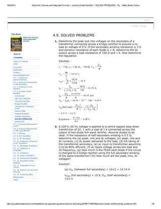
4.9. SOLVED PROBLEMS
1. Determine the peak and rms voltages on the secondary of a
transformer connected across a bridge rectifier to provide a no
load dc voltage of 9 V. If the secondary winding resistance is 3 Ω
and dynamic resistance of each diode is 1 Ω, determine the dc
output across a load resistance of 100 Ω and 1 K. Also determine
the regulation.
Solution:
2. A 220 V, 60 Hz voltage is applied to a centre tapped step-down
transformer of 22: 1 with a load of 1 K connected across the
output of two-diode full-wave rectifier. Assume diodes to be
ideal. If the resistance of half-secondary winding is 0.5 Ω,
determine the (a) peak, rms and dc voltages, (b) peak, rms and
dc currents, (c) dc power delivered to the load, (d) VA rating of
the transformer secondary, (e) ac input to transformer assuming
it to be 80% efficient, (f) ac ripple voltage across the load and
its frequency, (g) How much is the PIVof each diode if the circuit
is changed to a bridge rectifier using the full secondary winding
of the same transformer? (h) How much are the peak, rms, dc
voltages?
Solution:
(a) Vm (between full secondary) = 10√2 = 14.14 V
vrms (full secondary) = 10 V, Vm (half secondary) =
7.07 V
2. 16/5/2014 Electronic Devices and Integrated Circuits > Junction Diode Rectifier > SOLVED PROBLEMS - Pg. : Safari Books Online
http://my.safaribooksonline.com/book/electrical-engineering/semiconductor-technology/9788177589788/junction-diode-rectifier/solved_problems-003 2/8
(c) DC power delivered the load = I2
DCRL = (4.495
mA)21 K = 20.2 mW
(d) VA rating of the transformer can be found out using
TUF.
(f) As the ripple voltage under consideration would be
the second harmonics because the magnitude of higher
harmonics will become much less than it. Hence, the ac
ripple voltage is expressed as
3. Calculate the VDC, IDC, Vr(rms), Irms through a 1 KΩ load
connected to a half-wave rectifier circuit shown in Fig. 4.29 (a).
Figure 4.29(a). Figure 4.29(a)
Figure 4.29(b). Figure 4.29(b)
3. 16/5/2014 Electronic Devices and Integrated Circuits > Junction Diode Rectifier > SOLVED PROBLEMS - Pg. : Safari Books Online
http://my.safaribooksonline.com/book/electrical-engineering/semiconductor-technology/9788177589788/junction-diode-rectifier/solved_problems-003 3/8
Solution:
4. A sinusoidal voltage of 22 V, 50 Hz is applied to a half-wave
rectifier in Fig. 4.29(a) with dynamic resistance of the diode of
1 W. Calculate the maximum dc and rms currents flowing
through the load. Also calculate the dc output power developed,
ac-input power supplied, rectification efficiency, and ripple
factor.
Solution:
5. A 230 V−0−230 V input voltage is connected to a full-wave
rectifier shown in Fig. 4.30. Calculate the dc, ac voltages, dc
and ac power developed across the load. Also calculate the dc,
rms currents that will flow through the load.
Solution:
Figure 4.30. Figure 4.30
4. 16/5/2014 Electronic Devices and Integrated Circuits > Junction Diode Rectifier > SOLVED PROBLEMS - Pg. : Safari Books Online
http://my.safaribooksonline.com/book/electrical-engineering/semiconductor-technology/9788177589788/junction-diode-rectifier/solved_problems-003 4/8
Pin(ac) = V2
rmsRL = 2302 × 1 K = 52.9 W
6. Obtain number of turns in the primary and secondary of a
transformer connected in Fig. 4.31 to develop a dc voltage of 10
V across a load off 1 KΩ. What is the frequency of the ac voltage
present across the load?
Figure 4.31. Figure 4.31
Solution:
Figure 4.32. Figure 4.32
If there are 100 turns in the primary, then it must have 10 turns
in the secondary.
Frequency of the ac voltage present across the load = fin = 50
Hz.
7. Calculate the ripple factor without and with capacitor filter in
Fig. 4.32.
Solution:
5. 16/5/2014 Electronic Devices and Integrated Circuits > Junction Diode Rectifier > SOLVED PROBLEMS - Pg. : Safari Books Online
http://my.safaribooksonline.com/book/electrical-engineering/semiconductor-technology/9788177589788/junction-diode-rectifier/solved_problems-003 5/8
Theoretical ripple factor including filter =
8. What is the value of VDC and Vac developed across the load in
circuit of Fig. 4.33 assuming all diodes to be ideal. What is the
frequency of ac voltage present across load?
Figure 4.33. Figure 4.33
Solution:
Frequency of the ac voltage present across the load = 2fin = 100
Hz.
9. Design a full-wave rectifier with LC filter to provide 10 V dc at
100 mA along with maximum ripple of 2%. The frequency of
input voltage is 50 Hz. Determine the ripple factor of the LC
filter.
Solution:
10. Figure 4.34 is the output waveform of a half-wave rectifier with
6. 16/5/2014 Electronic Devices and Integrated Circuits > Junction Diode Rectifier > SOLVED PROBLEMS - Pg. : Safari Books Online
http://my.safaribooksonline.com/book/electrical-engineering/semiconductor-technology/9788177589788/junction-diode-rectifier/solved_problems-003 6/8
capacitor filter. The value of the capacitor is 1000 μF and the
value of load resistance is 100 Ω with frequency of input voltage
equal to 50 Hz. Determine the ripple factor and dc voltage.
Figure 4.34. Figure 4.34
Solution:
Ripple factor from theoretical expression is
11. Calculate the ripple factor in the case of a full-wave rectifier with
π-filter having the component values C1 = C2 = 500 μF and laod
resistance = 100 Ω.
Solution:
Expression for ripple factor = r =
Show that maximum dc power is transferred to the load in a full-
wave rectifier only when the dynamic resistance of the diode is
equal to the load resistance.
12. Design a full-wave rectifier with an LC filter that can yield dc
voltage of 9 V at 100 mA with a maximum ripple of 2%.
Solution:
7. 16/5/2014 Electronic Devices and Integrated Circuits > Junction Diode Rectifier > SOLVED PROBLEMS - Pg. : Safari Books Online
http://my.safaribooksonline.com/book/electrical-engineering/semiconductor-technology/9788177589788/junction-diode-rectifier/solved_problems-003 7/8
if LC is selected to be ten times higher than 0.13 H i.e. 1.3 H,
then C = 46 μF = 50 μF (standard value).
RB = 700Lmax = 700 × 1.3 H = 910Ω
Since RB is ten times higher than the load resistance RL = 90 Ω,
it will waste little power with the advantage of using L > LC.
13. A full-wave rectifier uses the LC filter as shown in Fig. 4.35
having the component values as L = 30 H, C = 25 μF. Calculate
the value of bleeder resistance required for the rectified voltage
= 250sin 100πt. If the value of load resistance is RL connected
in 10 KΩ, what would be the value of (a) filter dc output voltage,
(b) dc current through bleeder resistance, (c) dc current through
the load, (d) ripple factor?
Solution:
Value of bleeder resistance (load resistance is open) = RB = 3ωL
= 3 × 2πf × L = 28.3 KΩ
Figure 4.35. Figure 4.35
8. 16/5/2014 Electronic Devices and Integrated Circuits > Junction Diode Rectifier > SOLVED PROBLEMS - Pg. : Safari Books Online
http://my.safaribooksonline.com/book/electrical-engineering/semiconductor-technology/9788177589788/junction-diode-rectifier/solved_problems-003 8/8
Get instant access to over $1 million worth of books and videos.
You are currently reading a PREVIEW of this book.
Start a Free 10-Day Trial