Introduction to VLSIDesign
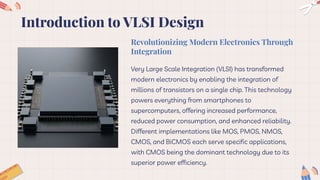
Very Large Scale Integration (VLSI) has transformed
modern electronics by enabling the integration of
millions of transistors on a single chip. This technology
powers everything from smartphones to
supercomputers, offering increased performance,
reduced power consumption, and enhanced reliability.
Different implementations like MOS, PMOS, NMOS,
CMOS, and BiCMOS each serve specific applications,
with CMOS being the dominant technology due to its
superior power efficiency.
Revolutionizing Modern Electronics Through
Integration
3.
Basic MOS TransistorOperation
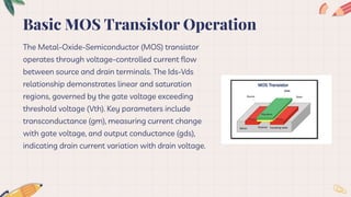
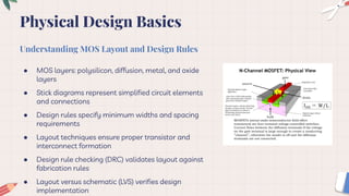
The Metal-Oxide-Semiconductor (MOS) transistor
operates through voltage-controlled current flow
between source and drain terminals. The Ids-Vds
relationship demonstrates linear and saturation
regions, governed by the gate voltage exceeding
threshold voltage (Vth). Key parameters include
transconductance (gm), measuring current change
with gate voltage, and output conductance (gds),
indicating drain current variation with drain voltage.
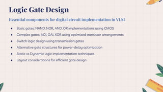
Logic Gate Design
Essentialcomponents for digital circuit implementation in VLSI
● Basic gates: NAND, NOR, AND, OR implementations using CMOS
● Complex gates: AOI, OAI, XOR using optimized transistor arrangements
● Switch logic design using transmission gates
● Alternative gate structures for power-delay optimization
● Static vs Dynamic logic implementation techniques
● Layout considerations for efficient gate design
9.
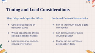
Timing and LoadConsiderations
Time Delays and Capacitive Effects
● Gate delays depend on
transistor sizing
● Wiring capacitance affects
signal propagation speed
● Load capacitance impacts
circuit performance
Fan-in and Fan-out Characteristics
● Fan-in: Maximum inputs a gate
can handle
● Fan-out: Number of gates
driven by output
● Higher fan-out increases
propagation delay
10.
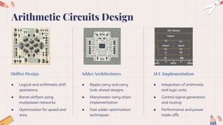
Arithmetic Circuits Design
ShifterDesign
● Logical and arithmetic shift
operations
● Barrel shifters using
multiplexer networks
● Optimization for speed and
area
Adder Architectures
● Ripple carry and carry
look-ahead designs
● Manchester carry chain
implementation
● Fast adder optimization
techniques
ALU Implementation
● Integration of arithmetic
and logic units
● Control signal generation
and routing
● Performance and power
trade-offs
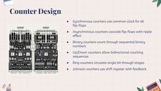
Counter Design
● Synchronouscounters use common clock for all
flip-flops
● Asynchronous counters cascade flip-flops with ripple
effect
● Binary counters count through sequential binary
numbers
● Up/Down counters allow bidirectional counting
sequences
● Ring counters circulate single bit through stages
● Johnson counters use shift register with feedback
2+2 = 4
13.
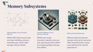
Memory Subsystems
Static RandomAccess Memory
(SRAM)
SRAM offers fast access times
and high reliability, using six
transistors per cell for data
storage without refresh.
Dynamic Random Access
Memory (DRAM)
DRAM uses single
transistor-capacitor pair per
cell, requiring periodic refresh
but achieving higher density
than SRAM.
ROM and Serial Memories
ROM provides permanent
storage while serial memories
offer sequential data access,
each optimized for specific
applications.
14.
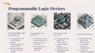
Programmable Array
Logic (PAL)
FieldProgrammable
Gate Arrays
Complex PLDs (CPLDs)
Programmable Logic Devices
Programmable Logic
Arrays (PLAs)
● Programmable AND
and OR arrays
● Flexible
implementation of
logic functions
● Higher complexity
but more versatile
design
● Fixed OR array with
programmable AND
● Faster operation
than PLAs
● Cost-effective for
simple logic
functions
● Configurable logic
blocks and
interconnects
● High flexibility in
design
implementation
● Reprogrammable
for different
● Multiple PAL-like
blocks with
interconnects
● Non-volatile
memory
configuration
● Suitable for
medium-complexity
15.
● Built-in Self-Test(BIST)
implementation
● Scan chain design for testability
● Fault simulation and coverage
analysis
● Automated Test Pattern
Generation (ATPG)
Key Testing Strategies
● Limited pin accessibility in
complex circuits
● High cost of comprehensive
testing
● Increased overhead for test
circuitry
● Time-consuming test pattern
generation
Common Testing Challenges
CMOS Testing Fundamentals
16.
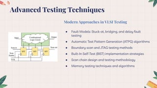
Advanced Testing Techniques
ModernApproaches in VLSI Testing
● Fault Models: Stuck-at, bridging, and delay fault
testing
● Automatic Test Pattern Generation (ATPG) algorithms
● Boundary scan and JTAG testing methods
● Built-In Self-Test (BIST) implementation strategies
● Scan chain design and testing methodology
● Memory testing techniques and algorithms