clipper and clamper are the application of semiconductor diodes
1.
Clipper and Clamper
Circuits
PresentedBy
DEBASISH MOHANTA
Assistant Professor
Department of Electrical Engineering
Government College of Engineering, Keonjhar
2.
Clipper
The clipperis a wave shaping network which control the shape of the output waveform by clipping
or removing some portion of the applied wave.
Clippers find extensive use in radar, digital and other electronic systems.
A clipper or limiter is used to clip off or remove a portion of the ac signal.
The half wave rectifier is basically a clipper that eliminates one of the alternations of an ac signal.
The important types of diode clippers are
i. Positive clipper
ii. Negative clipper
iii. Biased clipper
iv. Combination clipper
3.
Clipper
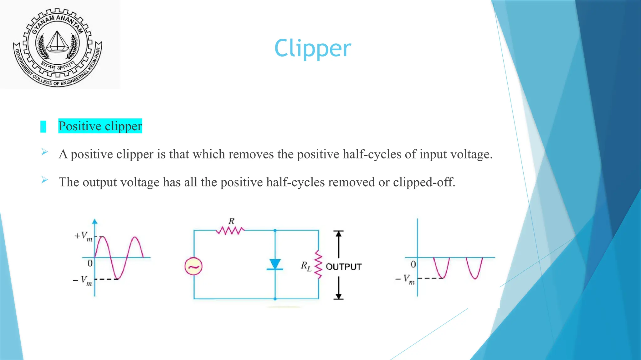
i. Positive clipper
A positive clipper is that which removes the positive half-cycles of input voltage.
The output voltage has all the positive half-cycles removed or clipped-off.
4.
Clipper
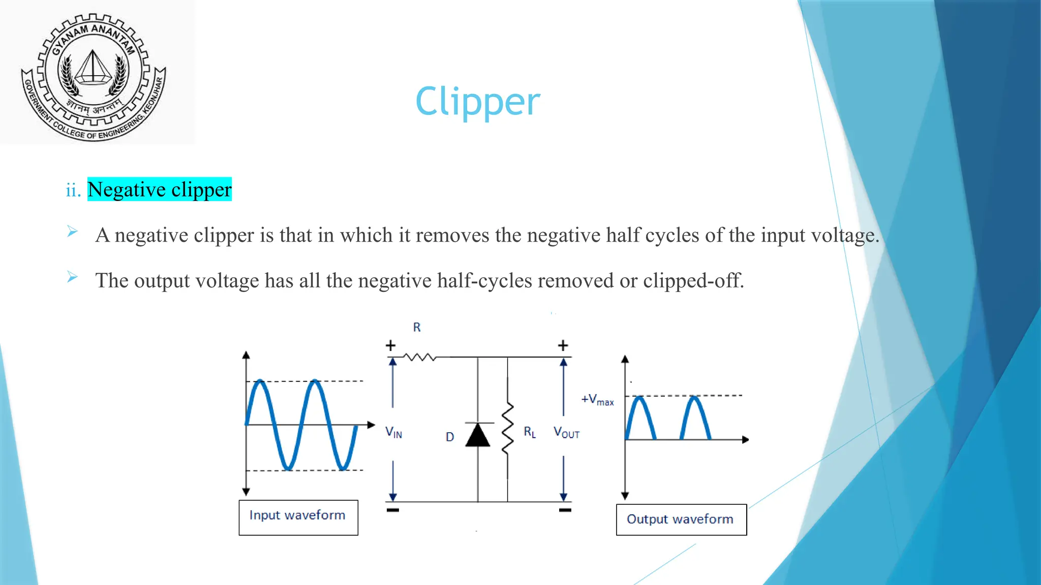
ii. Negative clipper
A negative clipper is that in which it removes the negative half cycles of the input voltage.
The output voltage has all the negative half-cycles removed or clipped-off.
5.
Clipper
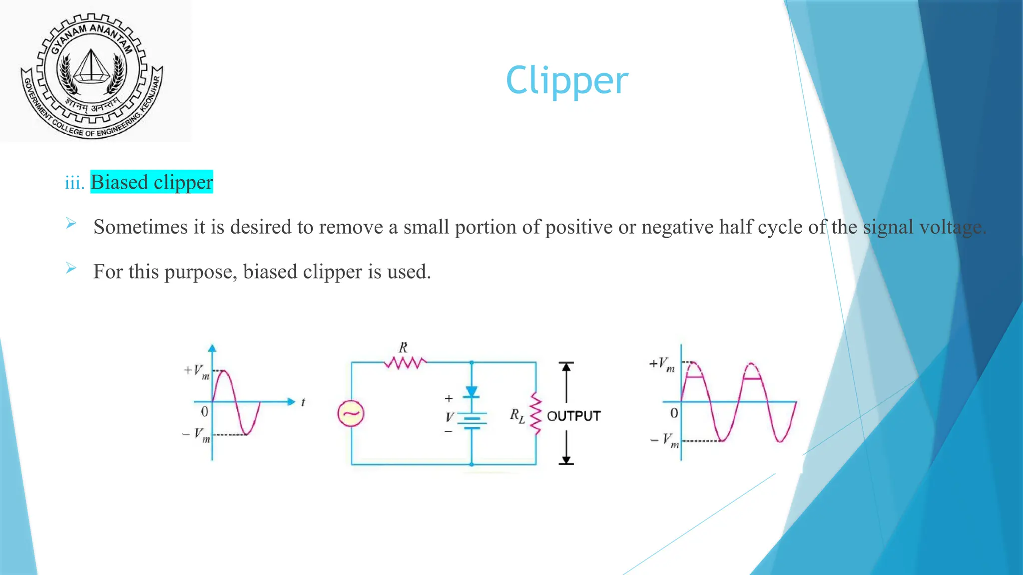
iii. Biased clipper
Sometimes it is desired to remove a small portion of positive or negative half cycle of the signal voltage.
For this purpose, biased clipper is used.
6.
Clipper
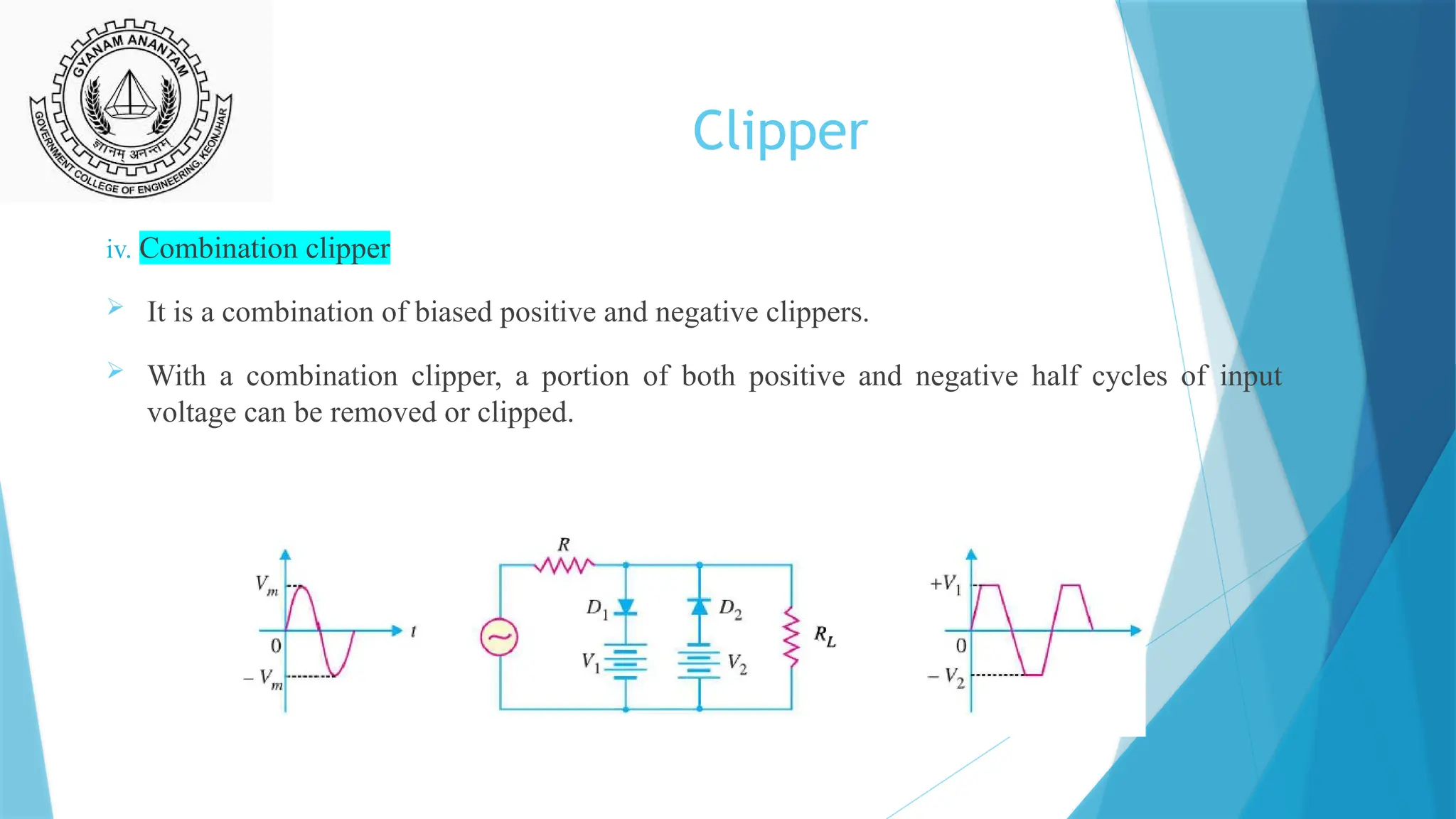
iv. Combination clipper
It is a combination of biased positive and negative clippers.
With a combination clipper, a portion of both positive and negative half cycles of input
voltage can be removed or clipped.
7.
Numerical
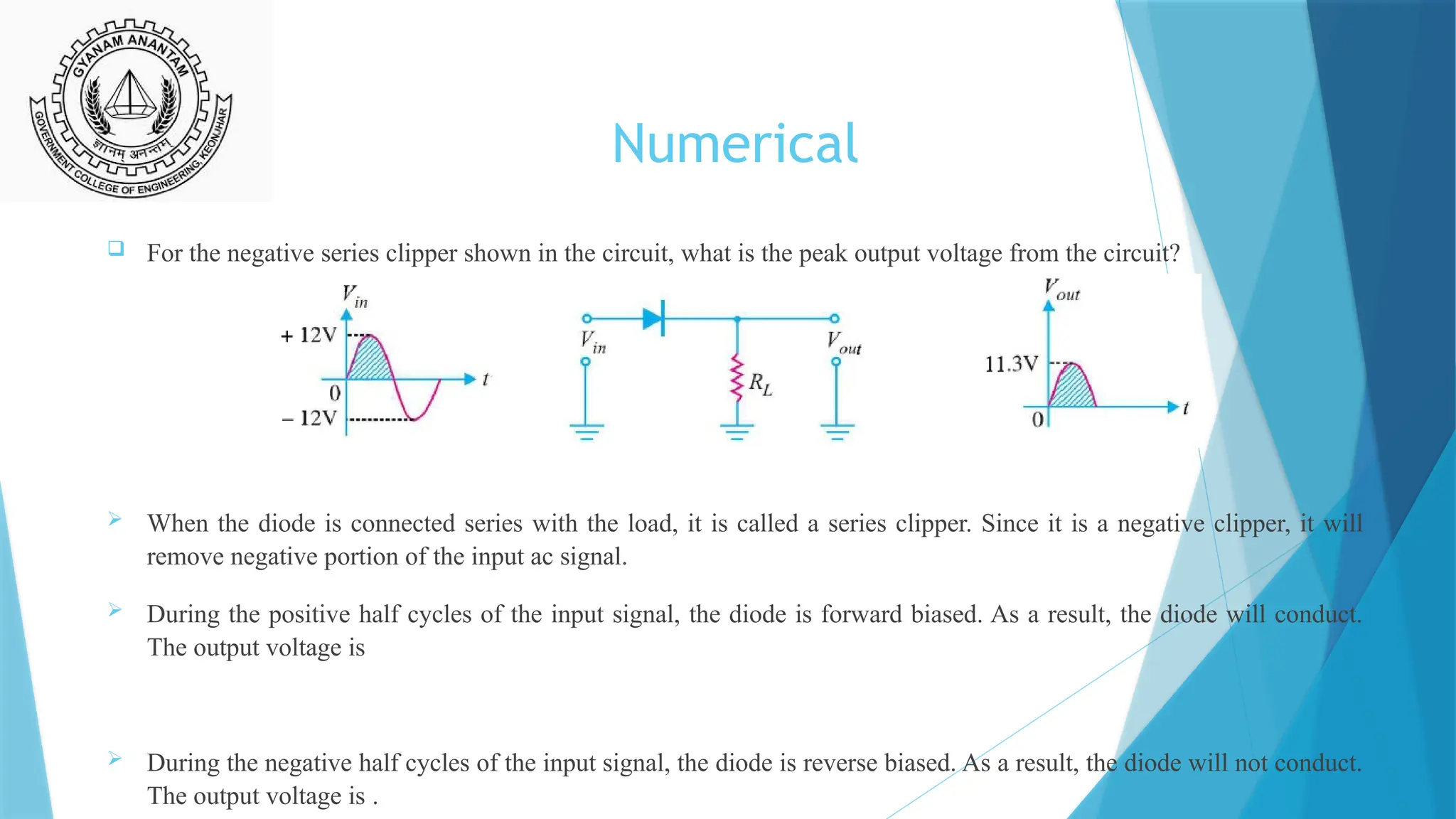
For thenegative series clipper shown in the circuit, what is the peak output voltage from the circuit?
When the diode is connected series with the load, it is called a series clipper. Since it is a negative clipper, it will
remove negative portion of the input ac signal.
During the positive half cycles of the input signal, the diode is forward biased. As a result, the diode will conduct.
The output voltage is
During the negative half cycles of the input signal, the diode is reverse biased. As a result, the diode will not conduct.
The output voltage is .
8.
Numerical
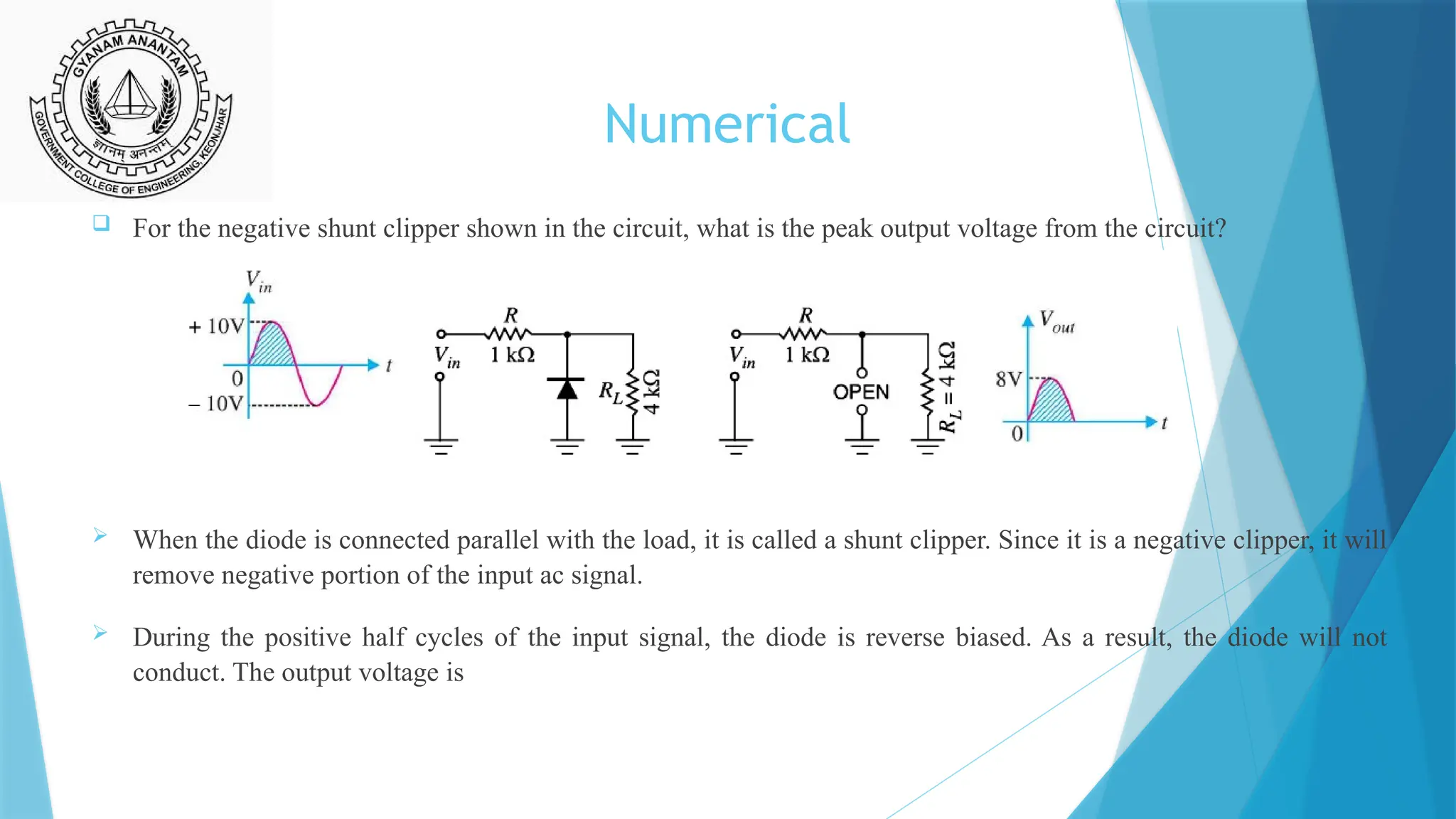
For thenegative shunt clipper shown in the circuit, what is the peak output voltage from the circuit?
When the diode is connected parallel with the load, it is called a shunt clipper. Since it is a negative clipper, it will
remove negative portion of the input ac signal.
During the positive half cycles of the input signal, the diode is reverse biased. As a result, the diode will not
conduct. The output voltage is
9.
Numerical
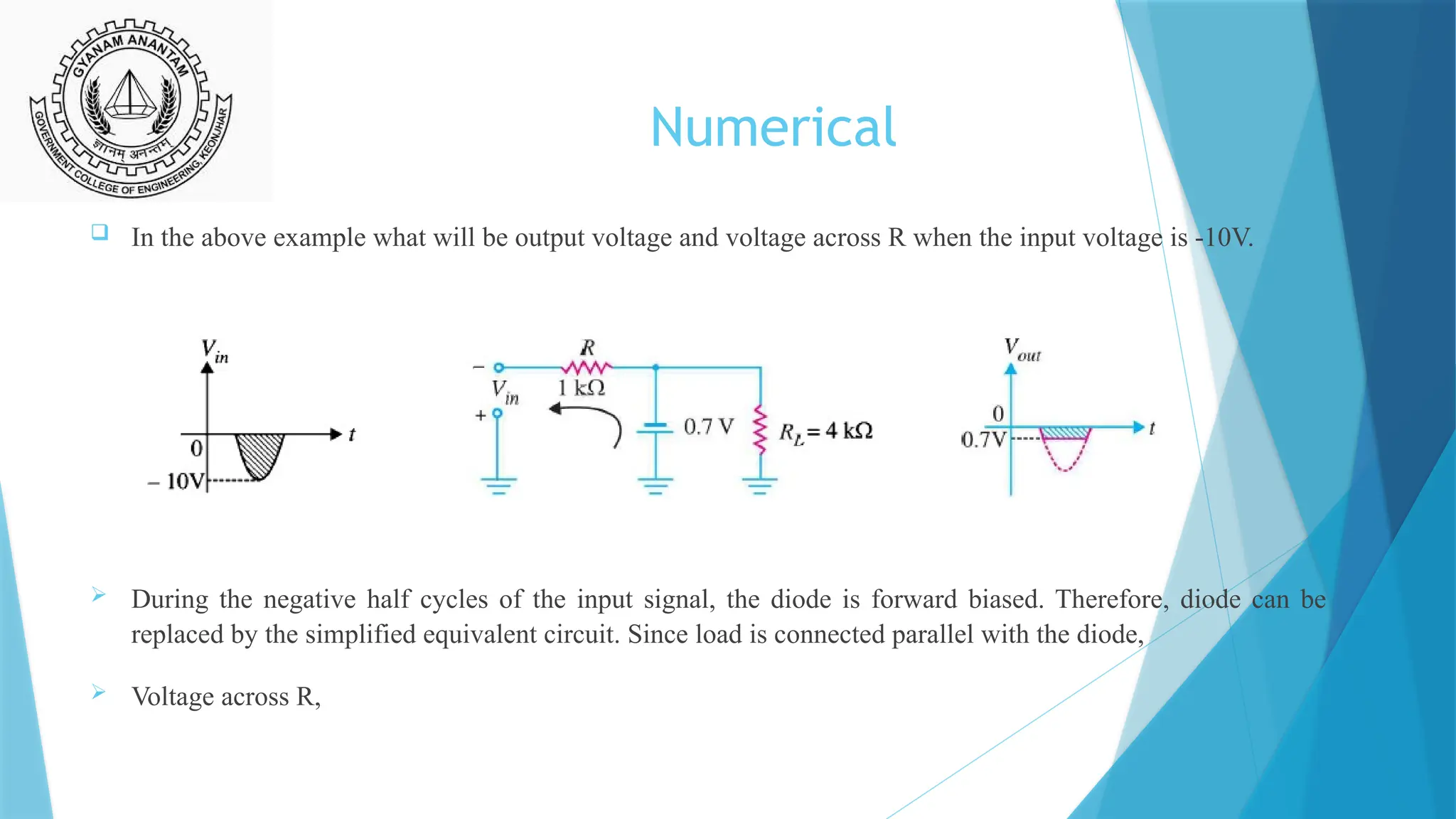
In theabove example what will be output voltage and voltage across R when the input voltage is -10V.
During the negative half cycles of the input signal, the diode is forward biased. Therefore, diode can be
replaced by the simplified equivalent circuit. Since load is connected parallel with the diode,
Voltage across R,
10.
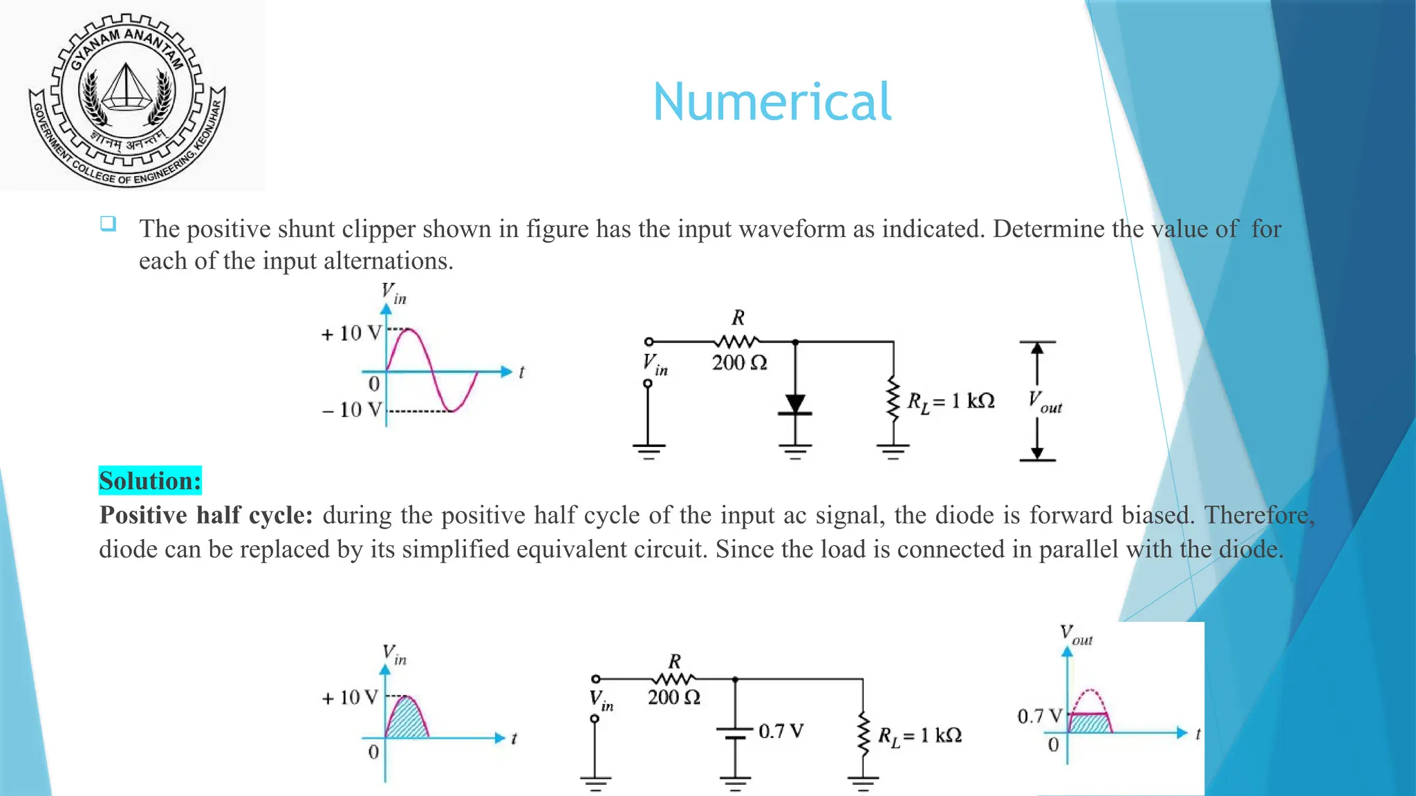
Numerical
The positiveshunt clipper shown in figure has the input waveform as indicated. Determine the value of for
each of the input alternations.
Solution:
Positive half cycle: during the positive half cycle of the input ac signal, the diode is forward biased. Therefore,
diode can be replaced by its simplified equivalent circuit. Since the load is connected in parallel with the diode.
11.
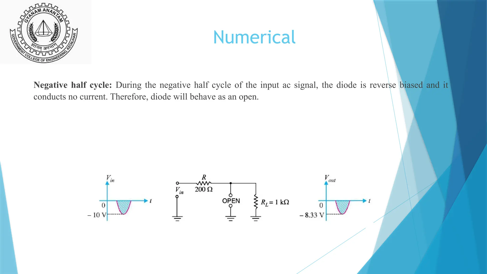
Numerical
Negative half cycle:During the negative half cycle of the input ac signal, the diode is reverse biased and it
conducts no current. Therefore, diode will behave as an open.
12.
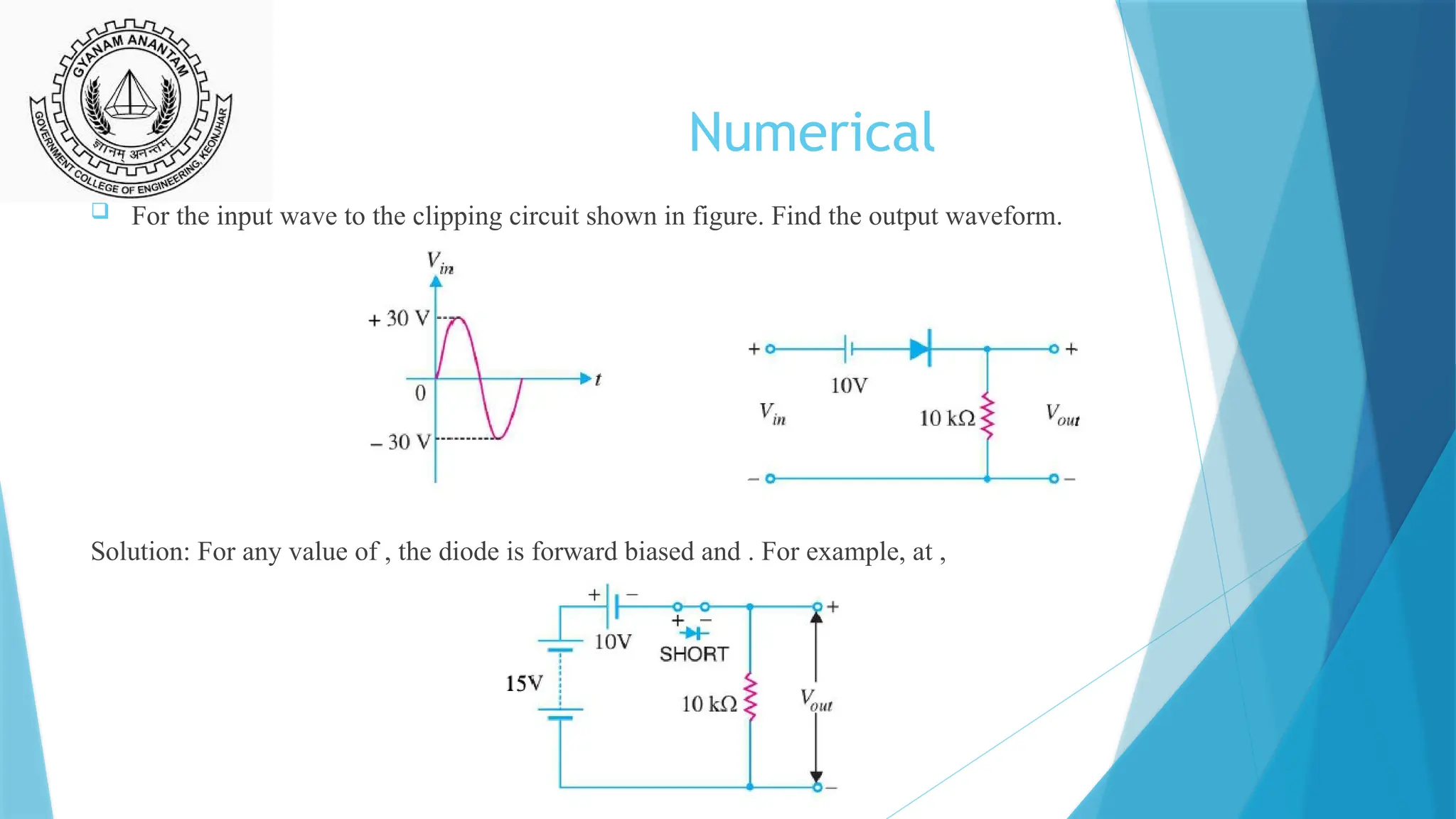
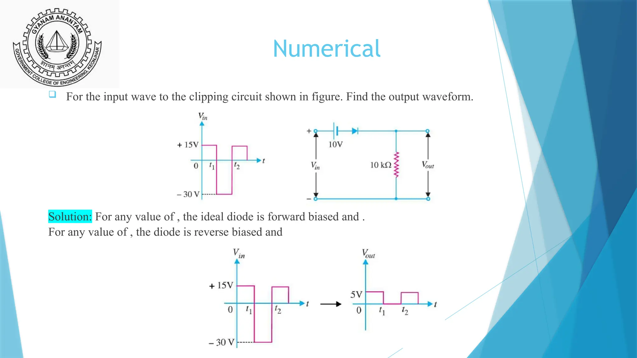
Numerical
For theinput wave to the clipping circuit shown in figure. Find the output waveform.
Solution: For any value of , the diode is forward biased and . For example, at ,
13.
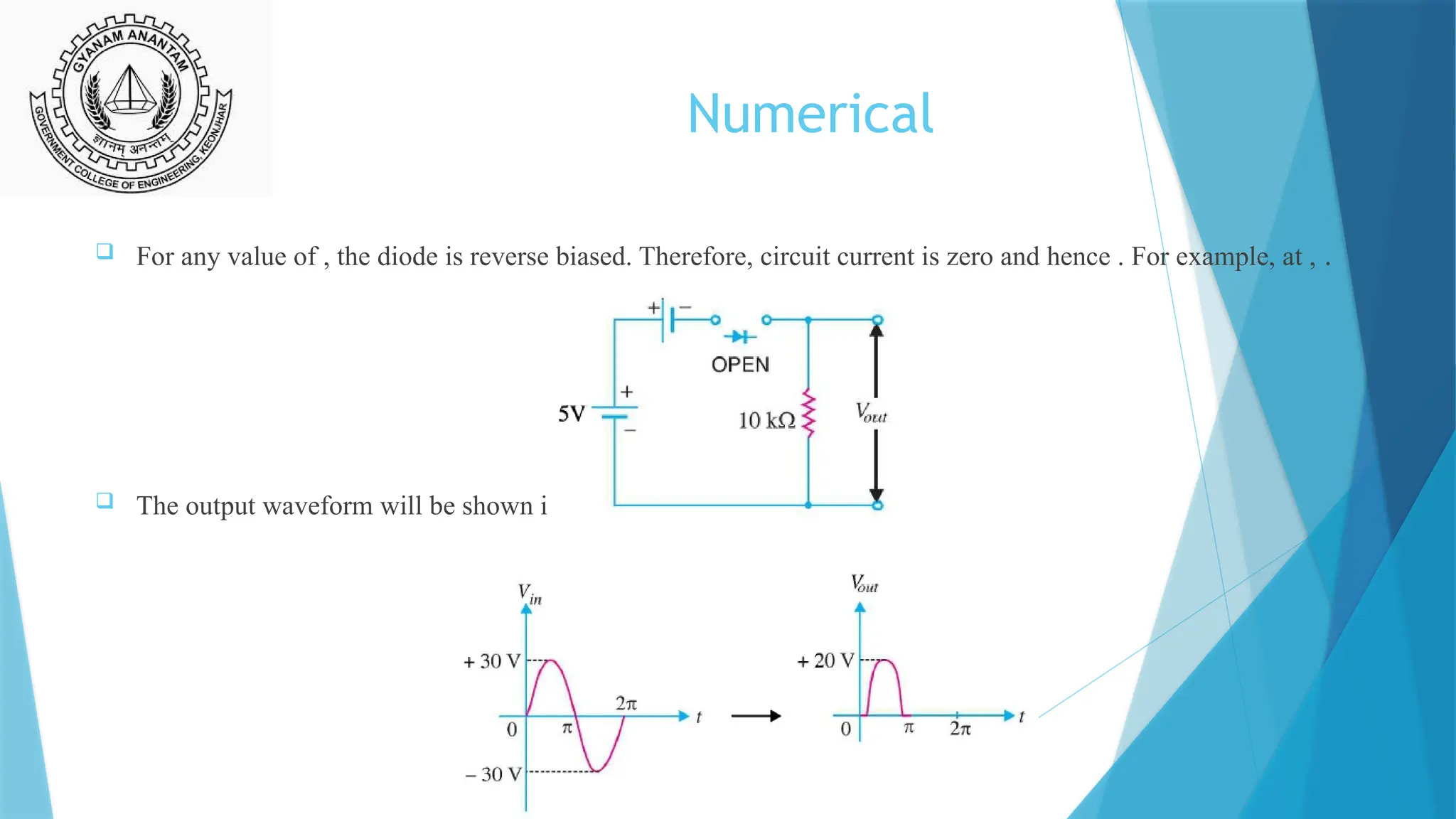
Numerical
For anyvalue of , the diode is reverse biased. Therefore, circuit current is zero and hence . For example, at , .
The output waveform will be shown in fig.
14.
Numerical
For theinput wave to the clipping circuit shown in figure. Find the output waveform.
Solution: For any value of , the ideal diode is forward biased and .
For any value of , the diode is reverse biased and
15.
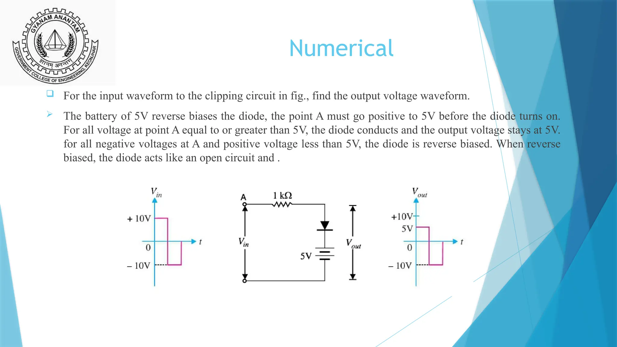
Numerical
For theinput waveform to the clipping circuit in fig., find the output voltage waveform.
The battery of 5V reverse biases the diode, the point A must go positive to 5V before the diode turns on.
For all voltage at point A equal to or greater than 5V, the diode conducts and the output voltage stays at 5V.
for all negative voltages at A and positive voltage less than 5V, the diode is reverse biased. When reverse
biased, the diode acts like an open circuit and .
16.
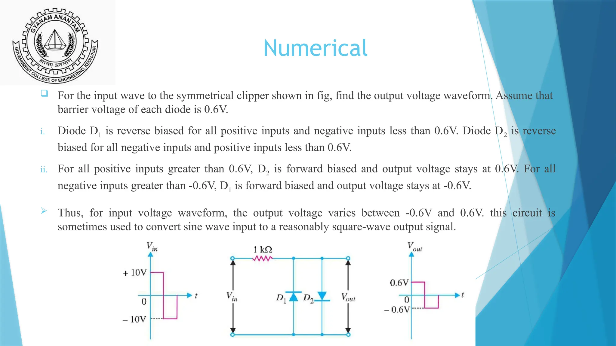
Numerical
For theinput wave to the symmetrical clipper shown in fig, find the output voltage waveform. Assume that
barrier voltage of each diode is 0.6V.
i. Diode D1 is reverse biased for all positive inputs and negative inputs less than 0.6V. Diode D2 is reverse
biased for all negative inputs and positive inputs less than 0.6V.
ii. For all positive inputs greater than 0.6V, D2 is forward biased and output voltage stays at 0.6V. For all
negative inputs greater than -0.6V, D1 is forward biased and output voltage stays at -0.6V.
Thus, for input voltage waveform, the output voltage varies between -0.6V and 0.6V. this circuit is
sometimes used to convert sine wave input to a reasonably square-wave output signal.
17.
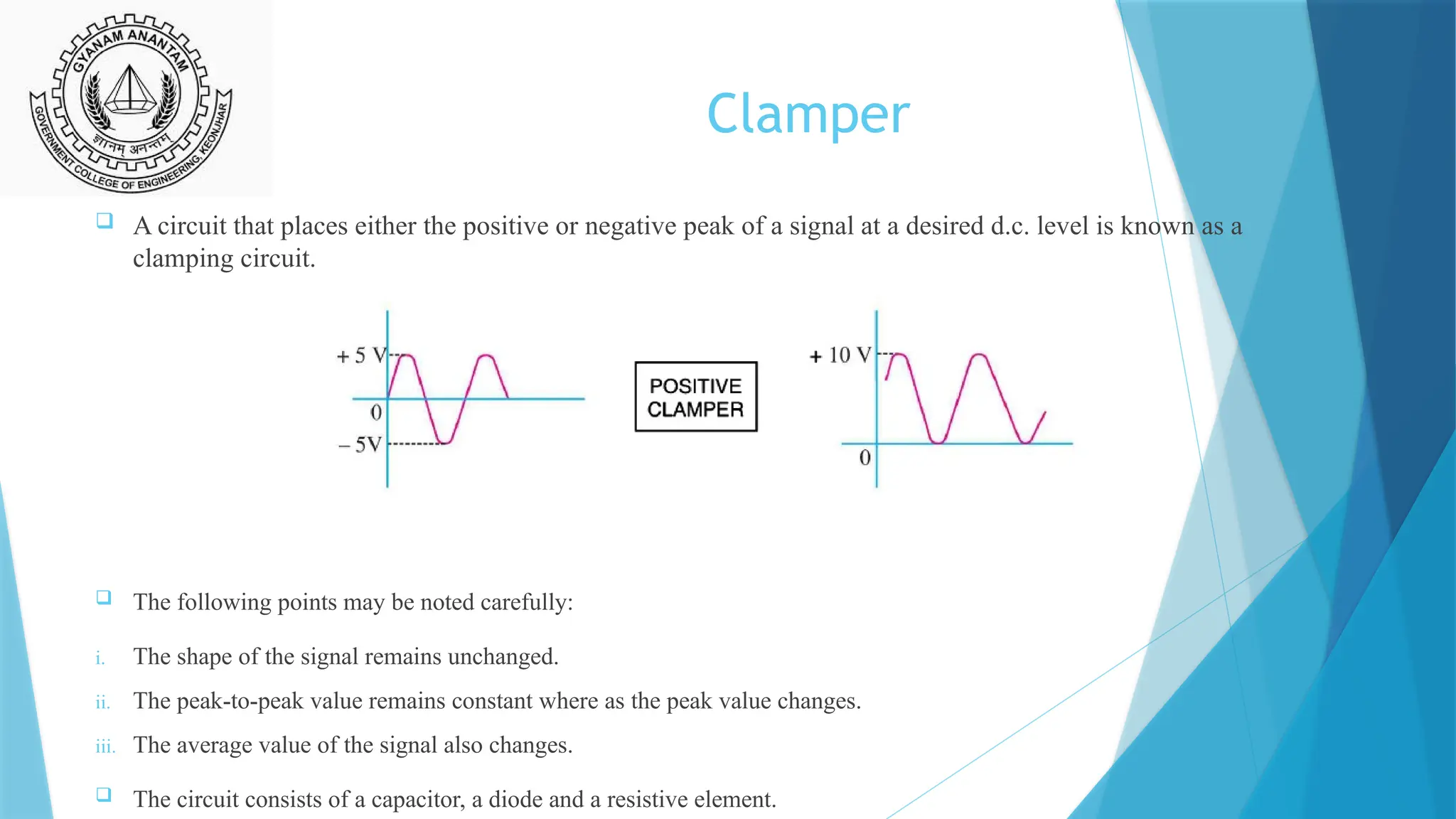
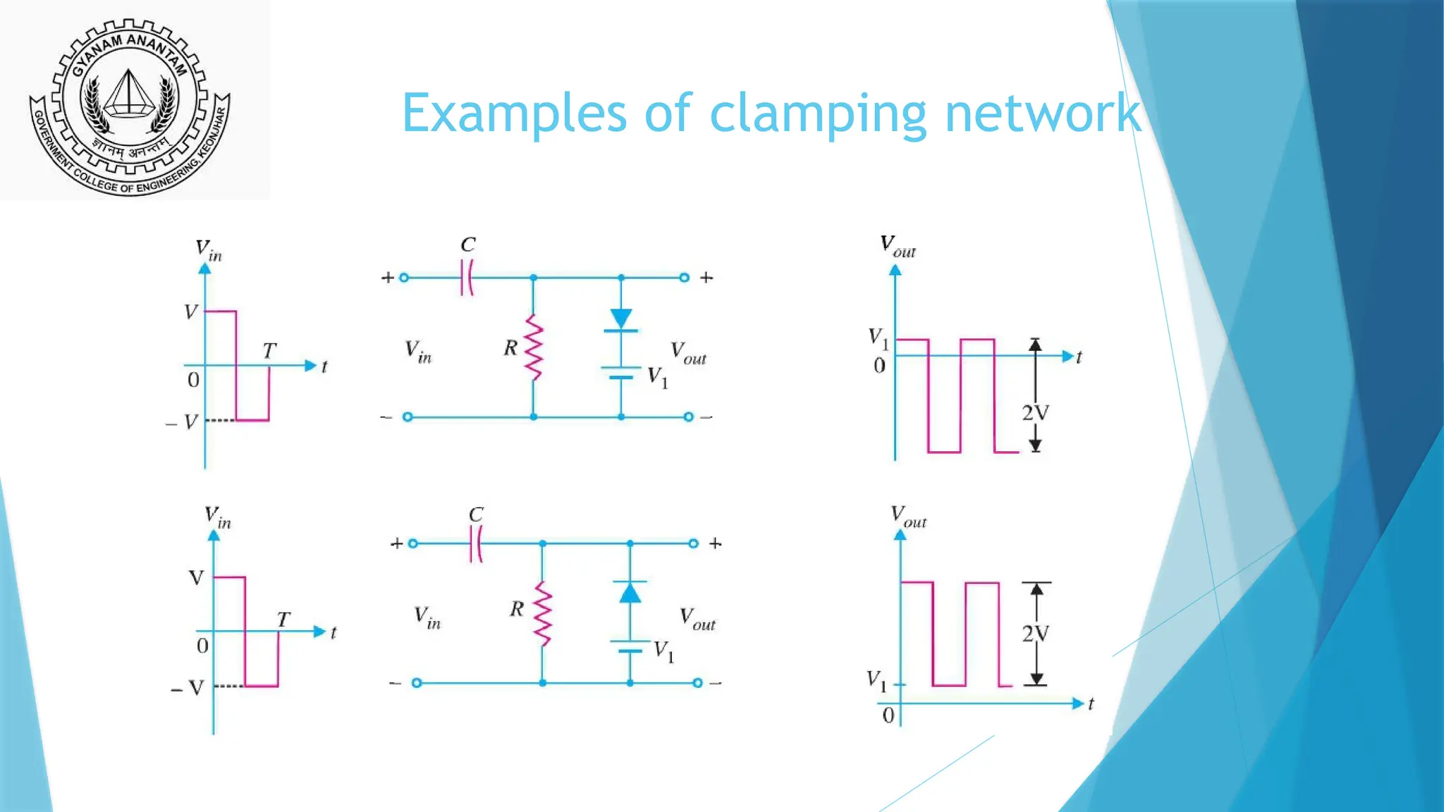
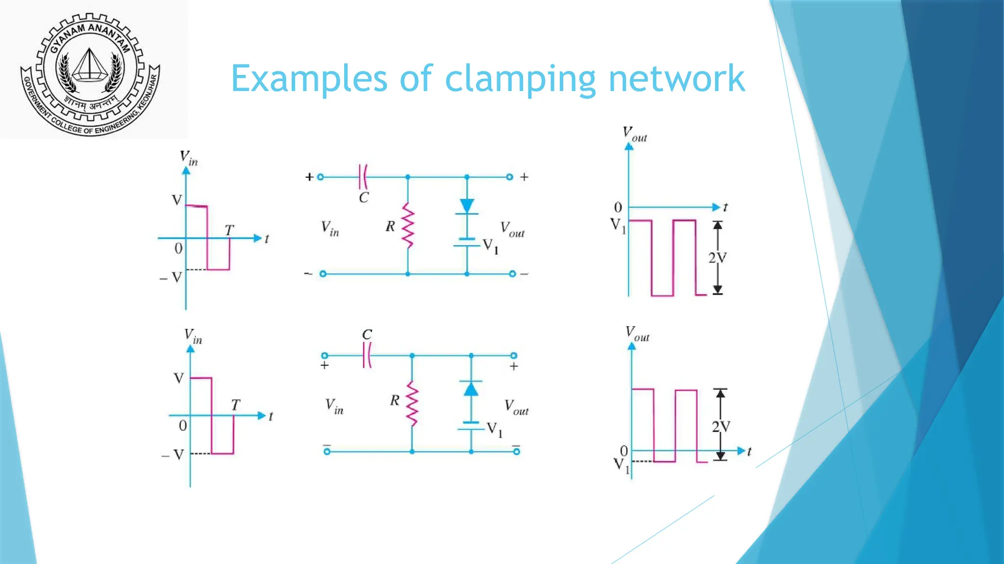
Clamper
A circuitthat places either the positive or negative peak of a signal at a desired d.c. level is known as a
clamping circuit.
The following points may be noted carefully:
i. The shape of the signal remains unchanged.
ii. The peak-to-peak value remains constant where as the peak value changes.
iii. The average value of the signal also changes.
The circuit consists of a capacitor, a diode and a resistive element.
18.
Analysis of clampingnetwork
i. Start the analysis of clamping network by considering the part of the input signal that will
forward bias the diode.
ii. Assume that during the period when the diode is in the ON state, the capacitor will charge to a
voltage level as determined by the network.
iii. Assume that during the period when the diode is in the OFF state, the capacitor will hold on to its
established voltage level.
iv. The total swing of the output must match the total swing of the input signal.
19.
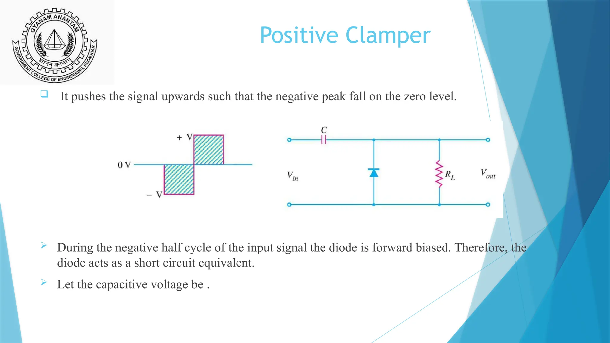
Positive Clamper
Itpushes the signal upwards such that the negative peak fall on the zero level.
During the negative half cycle of the input signal the diode is forward biased. Therefore, the
diode acts as a short circuit equivalent.
Let the capacitive voltage be .
Positive Clamper
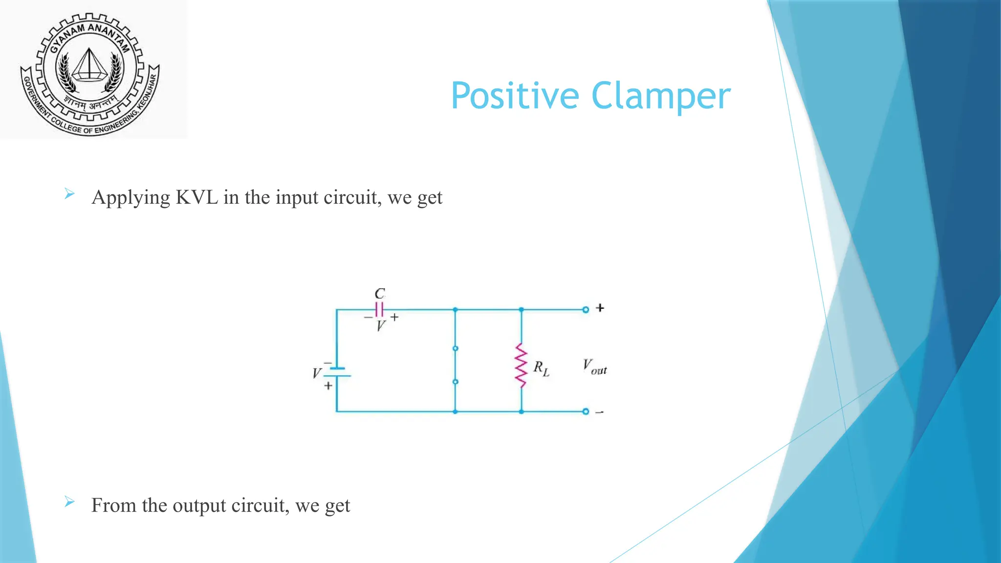
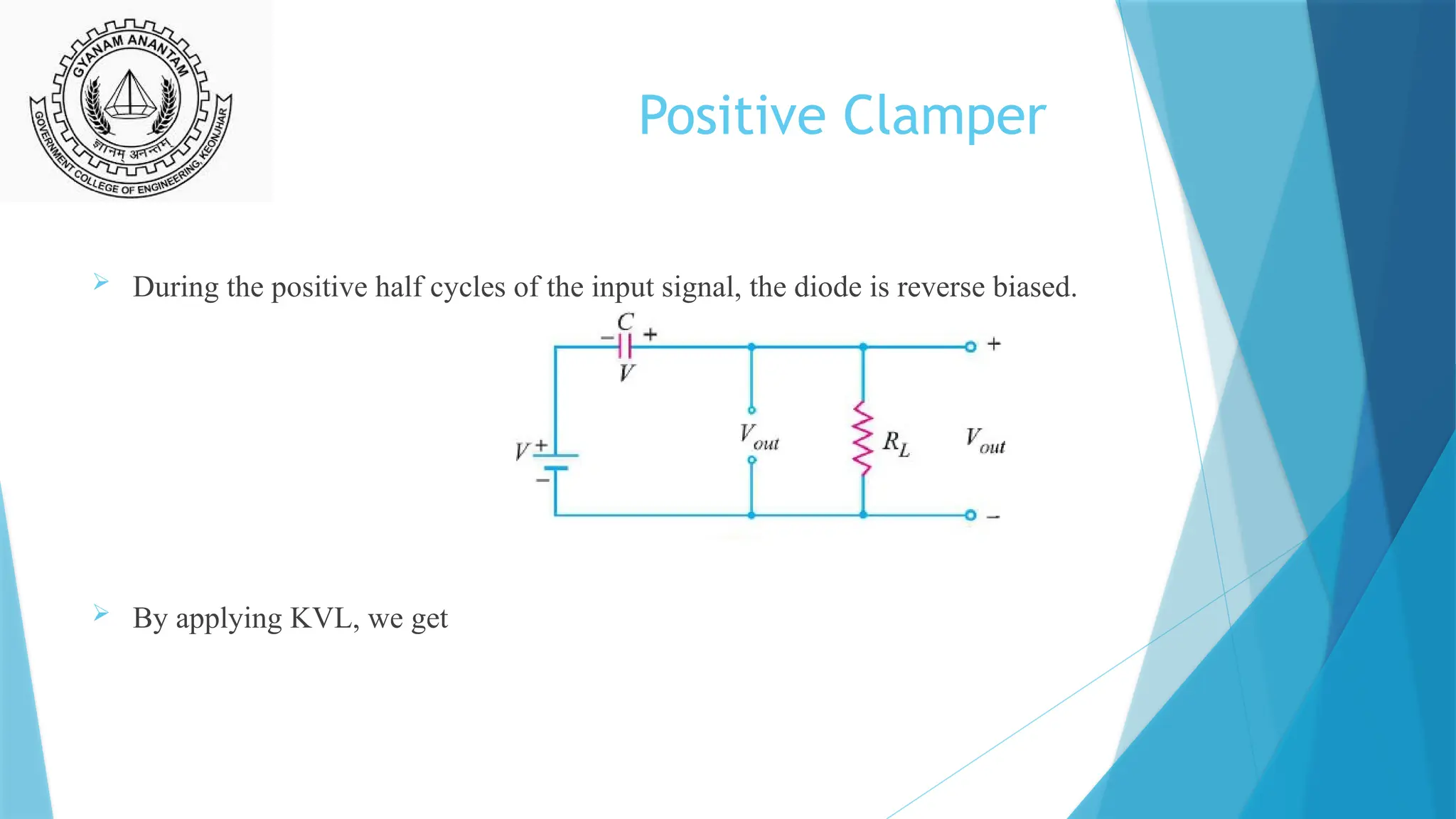
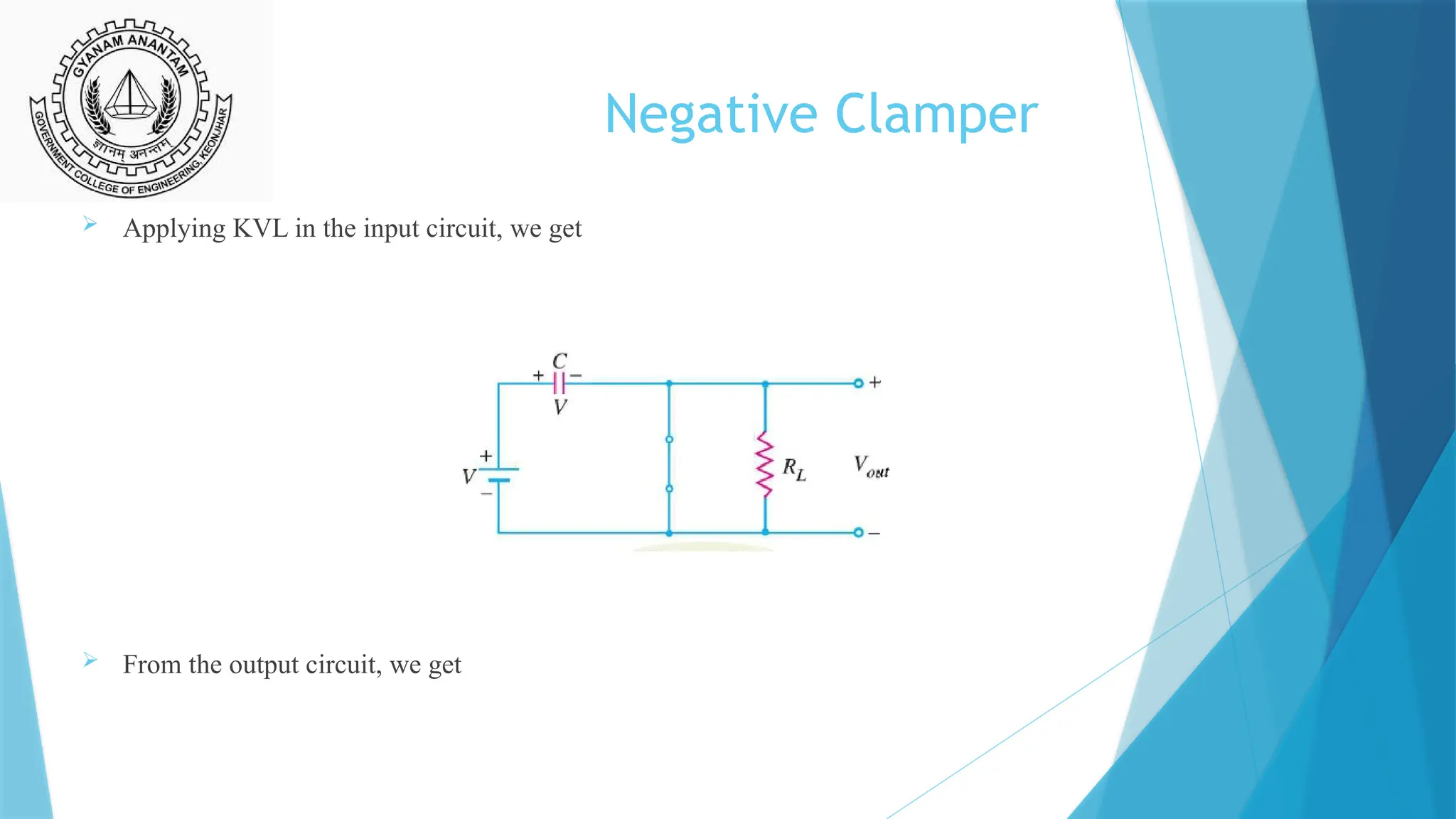
Duringthe positive half cycles of the input signal, the diode is reverse biased.
By applying KVL, we get
22.
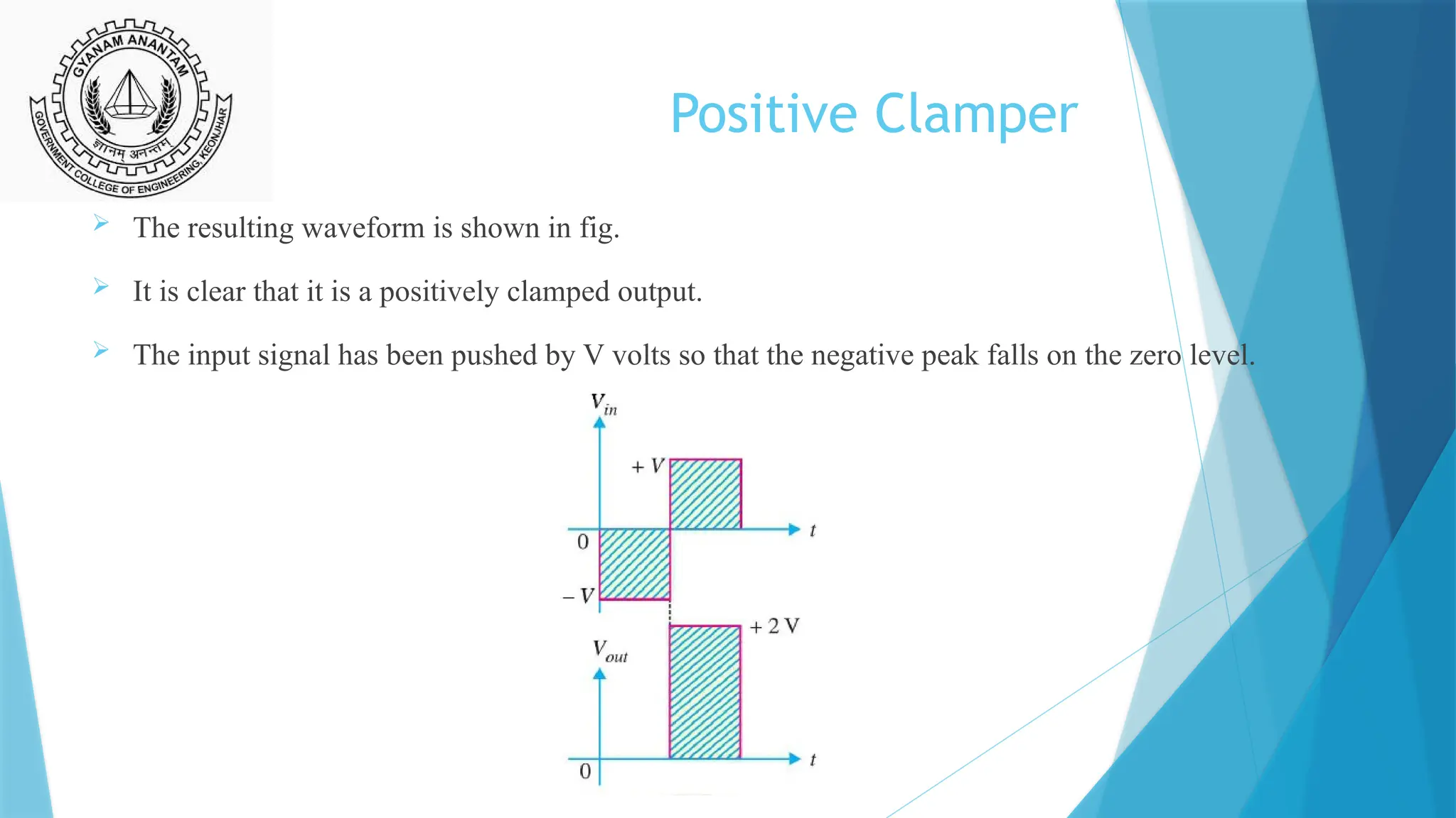
Positive Clamper
Theresulting waveform is shown in fig.
It is clear that it is a positively clamped output.
The input signal has been pushed by V volts so that the negative peak falls on the zero level.
23.
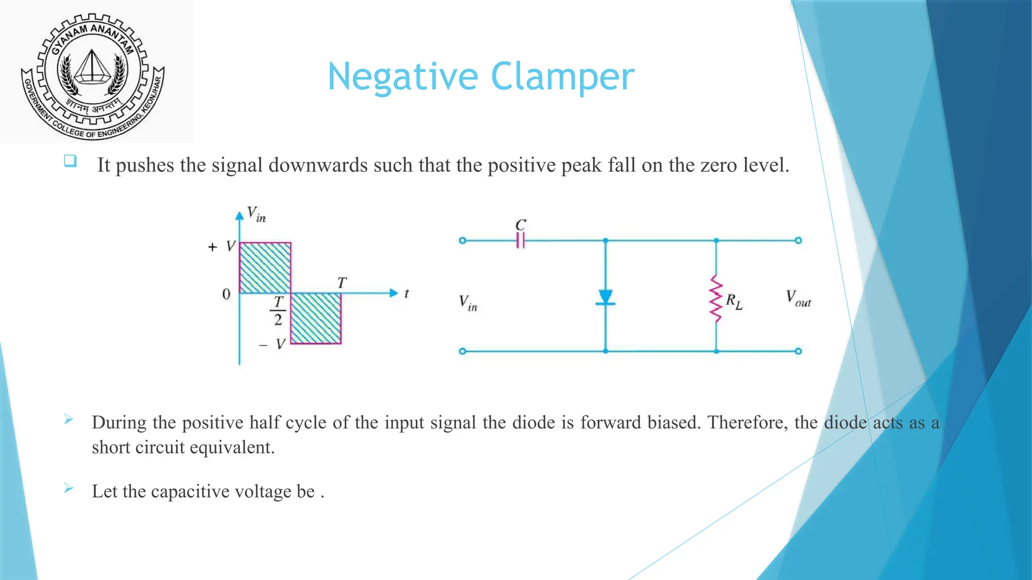
Negative Clamper
Itpushes the signal downwards such that the positive peak fall on the zero level.
During the positive half cycle of the input signal the diode is forward biased. Therefore, the diode acts as a
short circuit equivalent.
Let the capacitive voltage be .
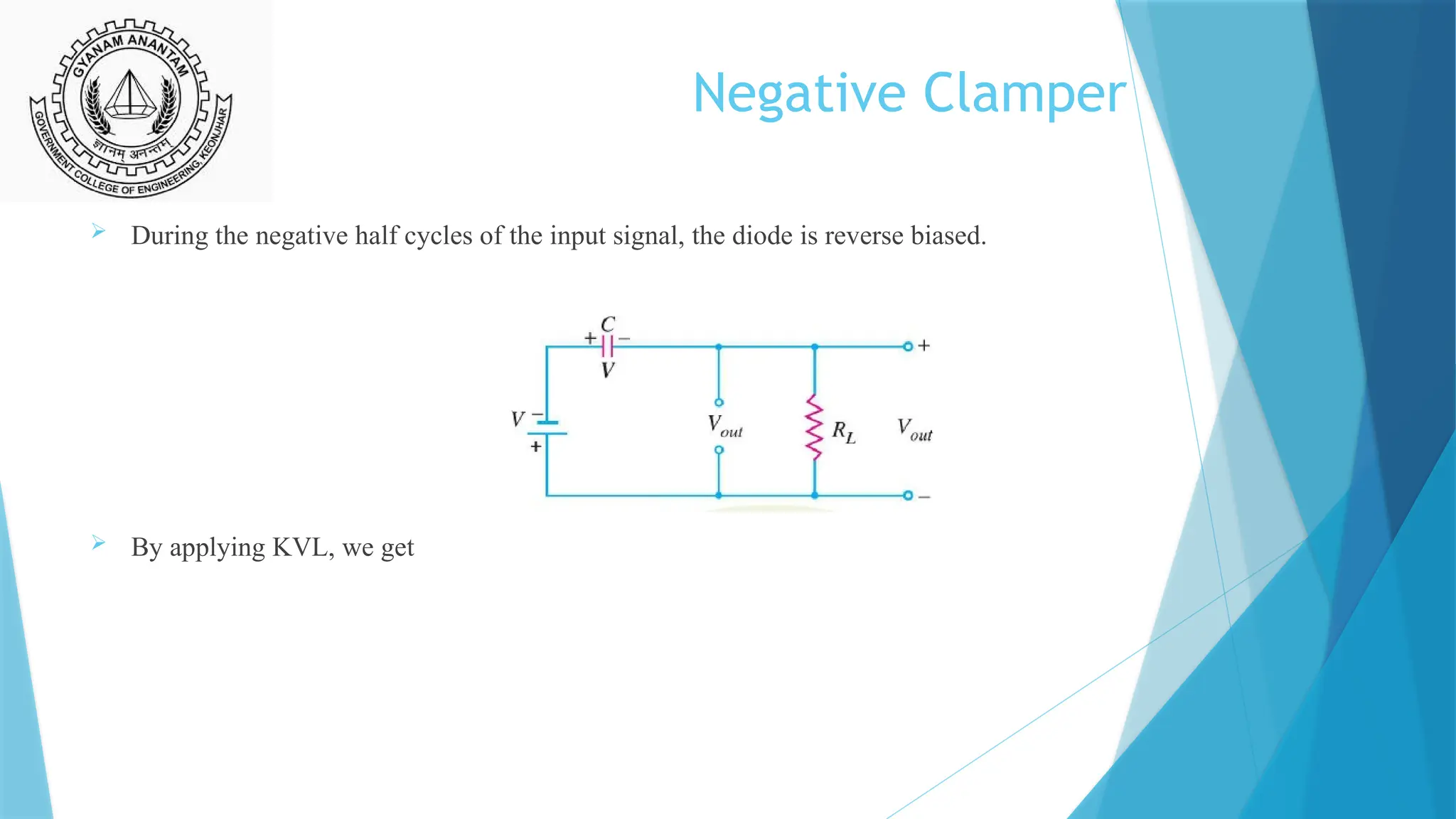
Negative Clamper
Duringthe negative half cycles of the input signal, the diode is reverse biased.
By applying KVL, we get
26.
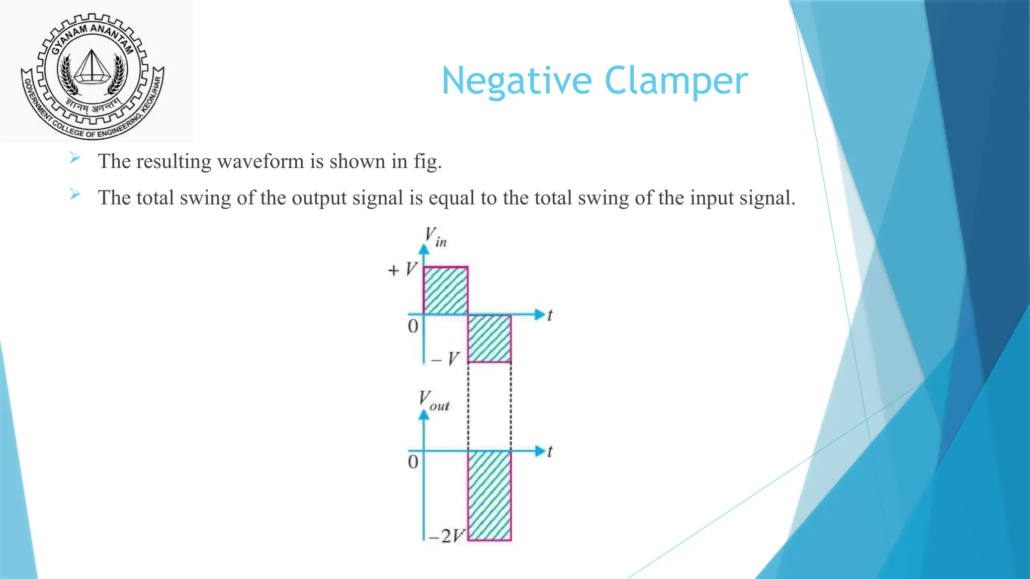
Negative Clamper
Theresulting waveform is shown in fig.
The total swing of the output signal is equal to the total swing of the input signal.
27.
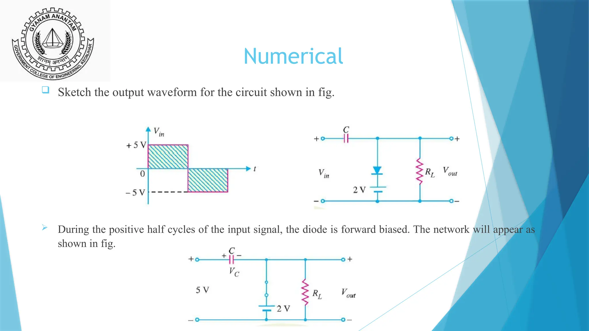
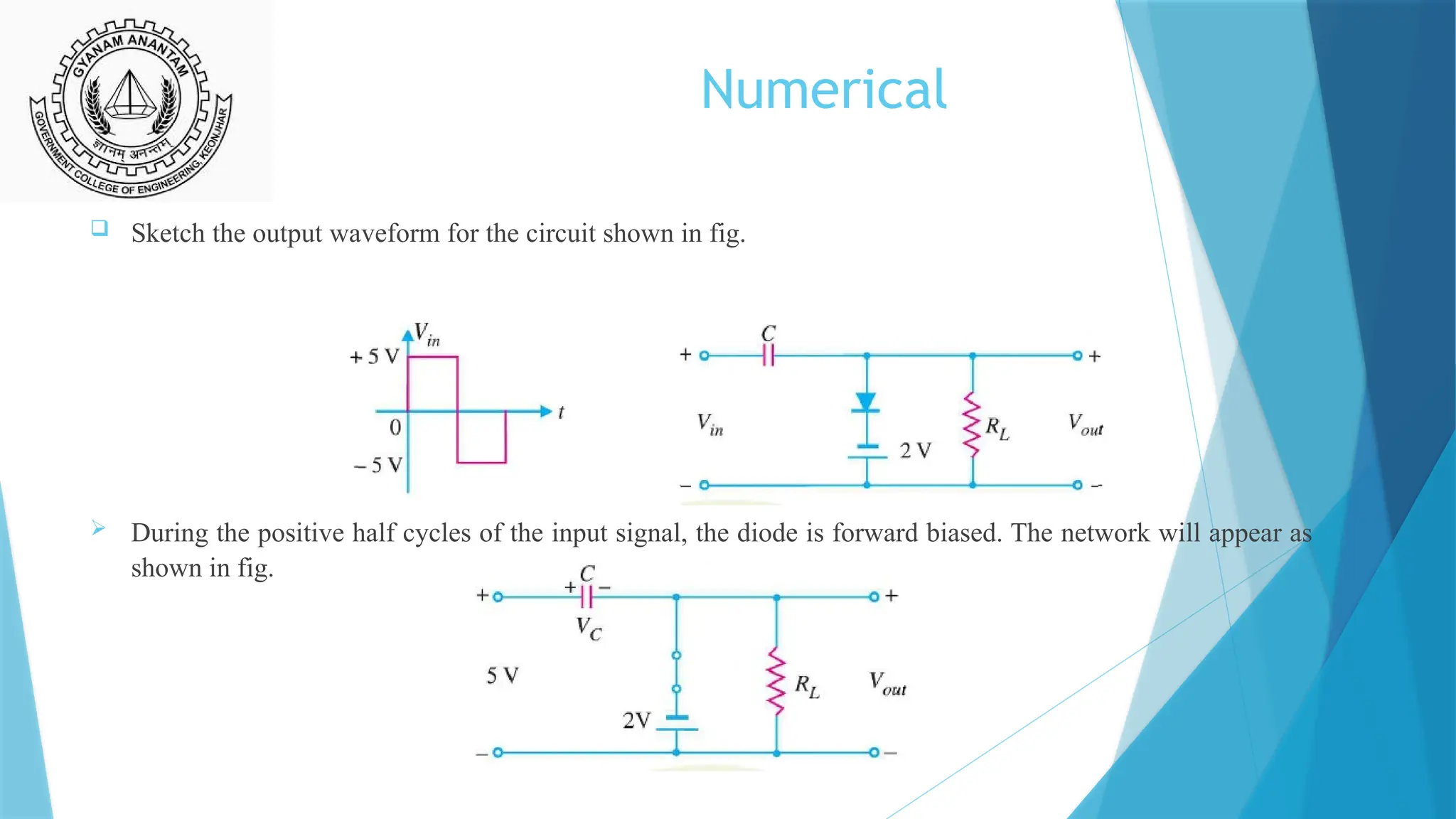
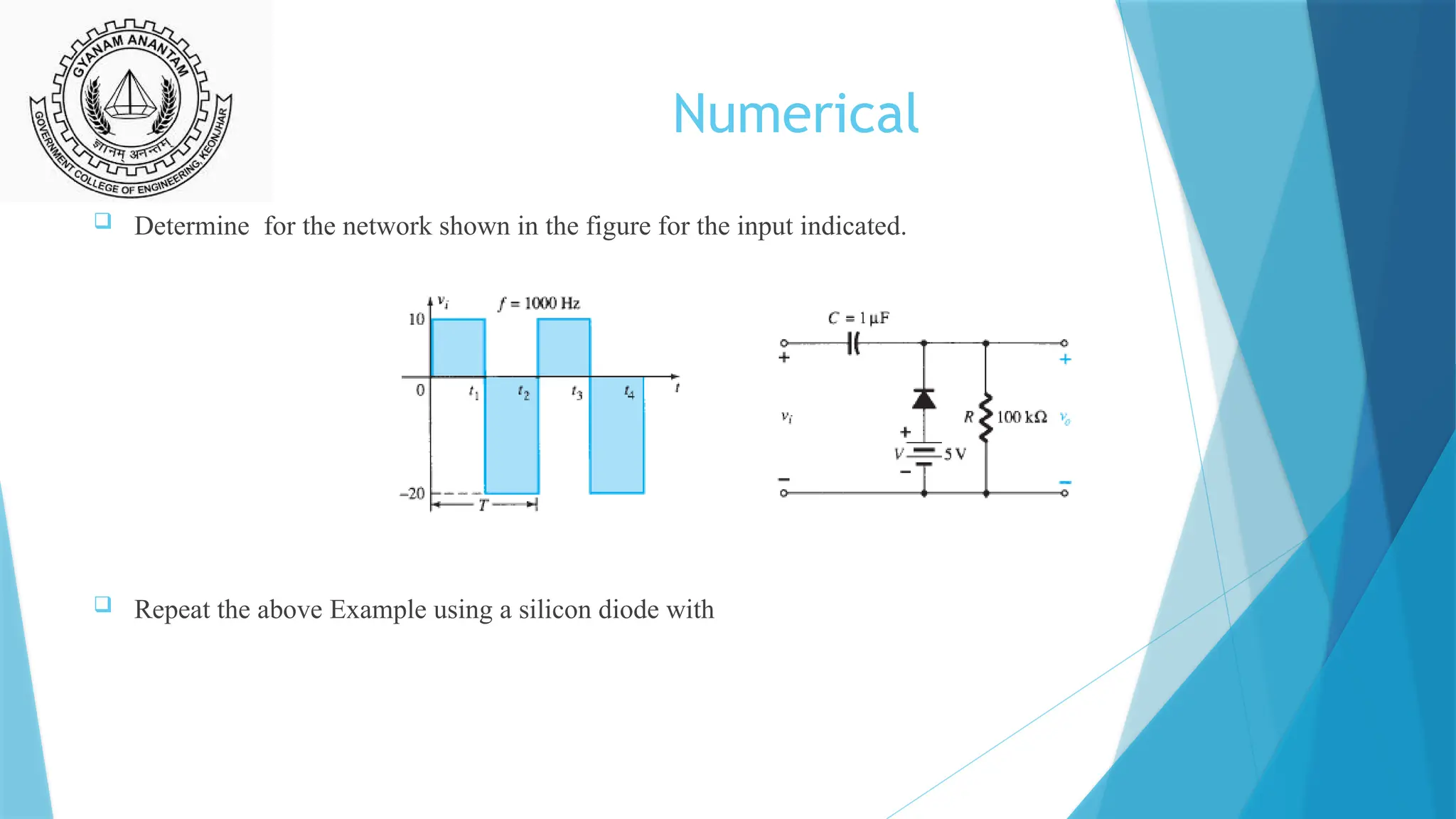
Numerical
Sketch theoutput waveform for the circuit shown in fig.
During the positive half cycles of the input signal, the diode is forward biased. The network will appear as
shown in fig.
28.
Numerical
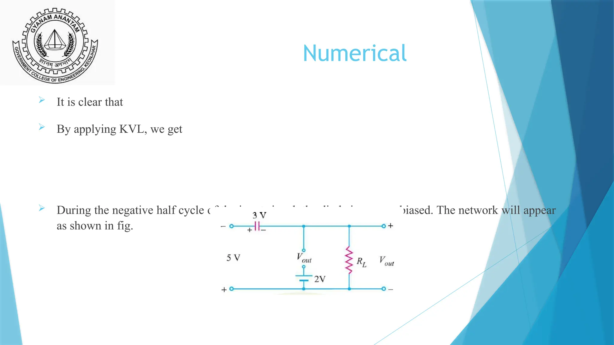
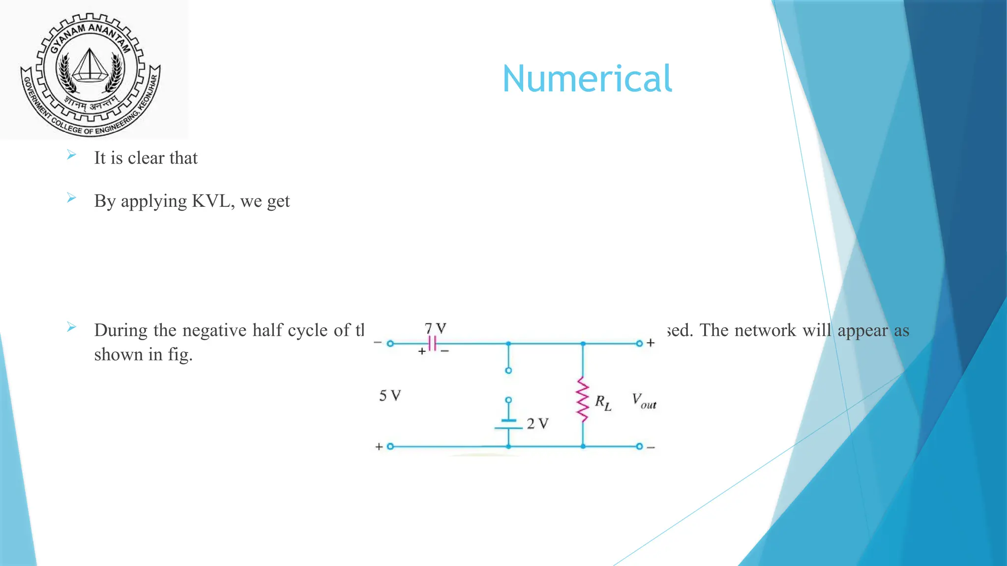
It isclear that
By applying KVL, we get
During the negative half cycle of the input signal, the diode is reverse biased. The network will appear
as shown in fig.
29.
Numerical
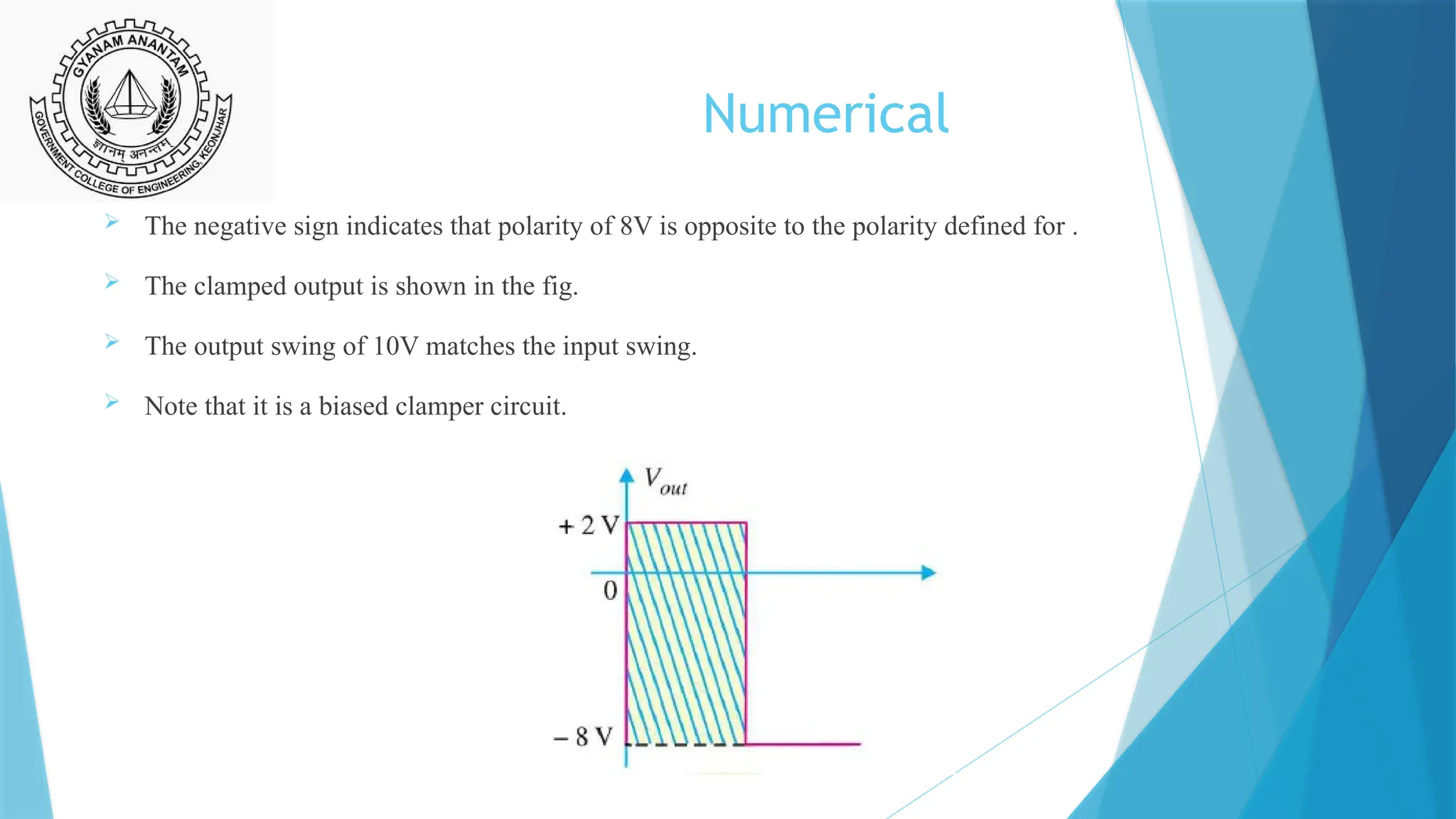
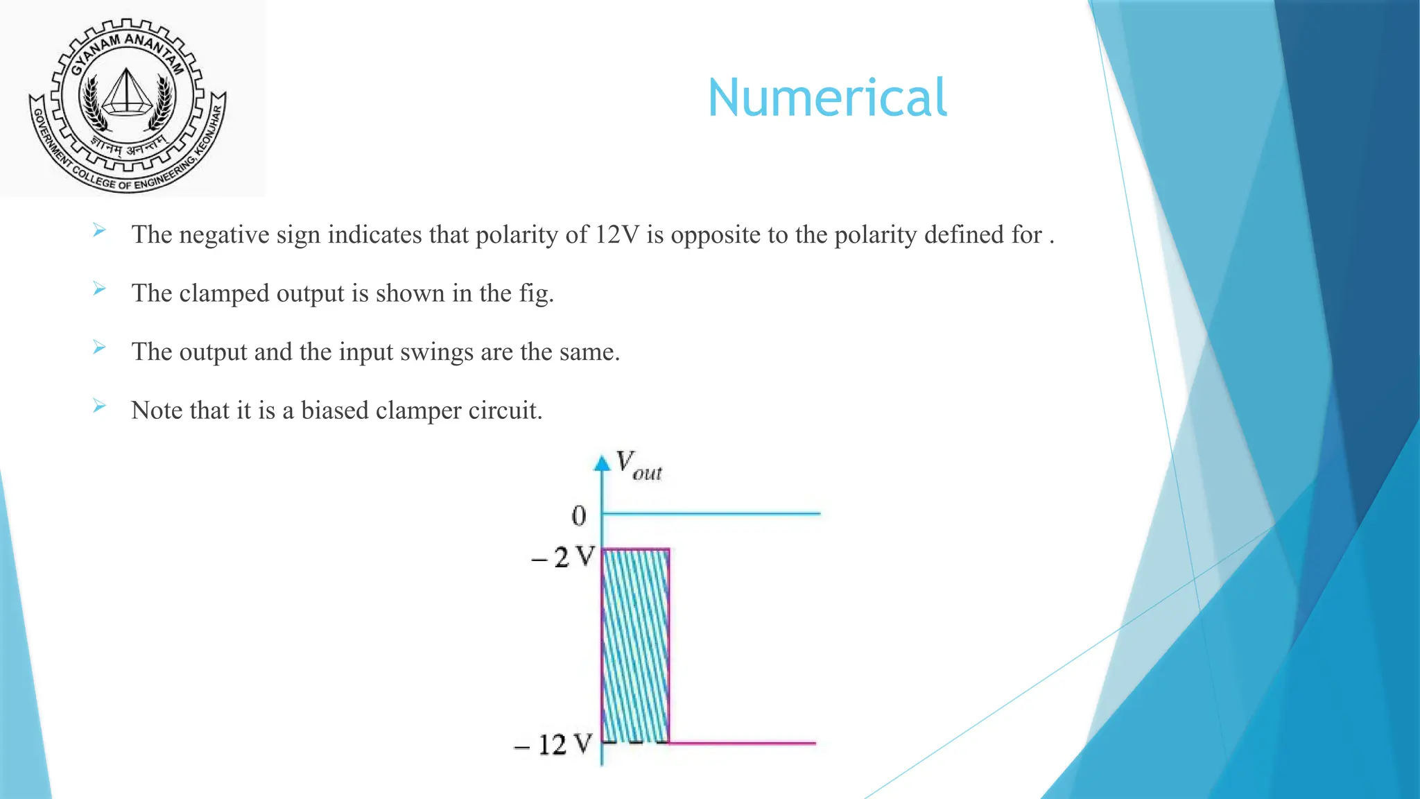
The negativesign indicates that polarity of 8V is opposite to the polarity defined for .
The clamped output is shown in the fig.
The output swing of 10V matches the input swing.
Note that it is a biased clamper circuit.
30.
Numerical
Sketch theoutput waveform for the circuit shown in fig.
During the positive half cycles of the input signal, the diode is forward biased. The network will appear as
shown in fig.
31.
Numerical
It isclear that
By applying KVL, we get
During the negative half cycle of the input signal, the diode is reverse biased. The network will appear as
shown in fig.
32.
Numerical
The negativesign indicates that polarity of 12V is opposite to the polarity defined for .
The clamped output is shown in the fig.
The output and the input swings are the same.
Note that it is a biased clamper circuit.