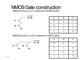
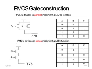
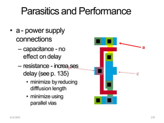
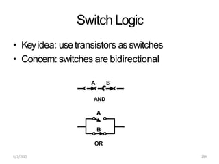
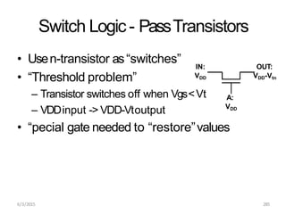
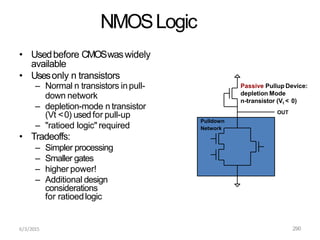
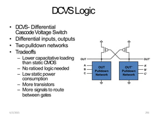
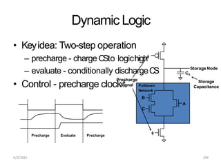
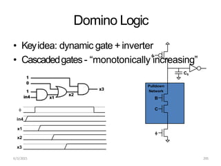
HAND TOOLS USED AT ELECTRONICS WORK PRESENTED BY KOUSTAV SARKAR
Gate level design, switch logic, pass transistors
1. 6/3/2015 274
UNIT-III
GA
TELEVELDESIGN
Topics
• Logic gates and other complexgates
• Switch logic
• Alternate gatecircuits
• Time delays
• Driving large capacitive loads
• Wiring capacitances
• Fan-in and fan-out, Choiceof layers
2. NMOSGate construction
A B
•NMOS devices in series implement a NAND function
A • B
A
B
6/3/2015
•NMOS devices in parallel implement a NOR function
A + B
A B F
0 0 1
0 1 1
1 0 1
1 1 0
A B F
0 0 1
0 1 0
1 0 0
1 1 0
275
3. PMOSGateconstruction
A B
•PMOS devices in parallel implement a NAND function
B
A
A + B
A • B
•PMOS devices in series implement a NOR function
A B F
0 0 1
0 1 1
1 0 1
1 1 0
6/3/2015
A B F
0 0 1
0 1 0
1 0 0
1 1 0
276
4. Parasitics and Performance
• Consider the
following layout:
• What is the impact
on performanceof
parasitics
– At point a(VDDrail)?
– At point b(input)?
– At Point c(output)?
b
a
c
6/3/2015 277
5. Parasitics and Performance
• a- power supply
connections
– capacitance - no
effect on delay
– resistance - increabses
delay (seep. 135)
• minimize byreducing
difffusion length
• minimize using
parallel vias
a
c
6/3/2015 278
6. Driving LargeLoads
• Off-chip loads, long wires, etc. have highcapacitance
• Increasing transistor sizeincreases driving ability
(and speed), but in turn increases gatecapacitance
• Solution: stagesof progressively largertransistors
– Usenopt =ln(Cbig/Cg).
– Scaleby afactor of a=e
6/3/2015 281
7. 6/3/2015 282
Summary: Static CMOS
• Advantages
– High Noise Margins (VOH=VDD,VOL=Gnd)
– No static power consumption (except for leakage)
– Comparable rise and fall times (with propersizing)
– Robust and easyto use
• Disadvantages
– Largetransistor counts (2N transistors for Ninputs)
• Larger area
• More parasitic loading (2 transistor gateson eachinput)
– Pullup issues
• Lower driving capability of Ptransistors
• Seriesconnections especially problematic
• Sizing helps, but increases loading on gate inputs
11. Switch Logic - Transmission Gates
A
A
6/3/2015 286
• Complementary transistors - n andp
• No threshold problem
• Cost: extra transistor, extra control input
• Not aperfect conductor!
A’
A’
13. ChargeSharing
• Consider transmission gates in series
– Eachnode hasparasitic capacitances
– Problems occur when inputs change to
redistribute charge
– Solution: design network sothere is always apath
from VDDor Gndto output
6/3/2015 288
14. Aside: Transmission Gatesin Analog
• Transmission Gates
work with analog values,too!
• Example:
Voltage-ScalingD/AConverter
6/3/2015 289
15. NMOSLogic
• Usedbefore CMOSwaswidely
available
• Usesonly n transistors
– Normal n transistors inpull-
down network
– depletion-mode n transistor
(Vt <0) usedfor pull-up
– "ratioed logic" required
• Tradeoffs:
– Simpler processing
– Smaller gates
– higher power!
– Additional design
considerations
for ratioedlogic
Passive Pullup Device:
depletion Mode
n-transistor (Vt < 0)
OUT
6/3/2015 290
Pulldown
Network
16. Pseudo-nmosLogic
• Sameidea, asnmos, but usep-
transistor for pullup
• "ratioed logic" required for
proper design (more about
this next)
• Tradeoffs:
– Fewer transistors -> smaller
gates, esp. for large number
of inputs
– lesscapacitative load on gates
that drive inputs
– larger powerconsumption
– lessnoise margin (VOL> 0)
– additional design
considerations due to ratioed
logic
Passive Pullup Device:
P-Transistor
OUT
Pulldown
Network
6/3/2015 291
17. Rationed Logicfor Pseudo-nmos
• Approach:
– AssumeVOUT=VOL=0.25*VDD
– Assume1 pulldown transistor ison
– Equate currents in p, ntransistors
– Solvefor ratio between sizesof p, n
transistors to get theseconditions
necessary for
– Further calculations
series connections
Idn I pn
1
k'
Wn
n L n
gs,n tn
2
V V 2
1
k'
Wp
p Lp
gs,p tp ds,p ds,p
2V V V V2
(EQ 3 21)
2
Wp
Wn
Ln
L p
3.9 (EQ 3 22) Assu ming V DD 3.3V
Idp
OUT
Pulldown
Network
Idn
6/3/2015 292
18. DCVSLogic
• DCVS- Differential
CascodeVoltage Switch
• Differential inputs, outputs
• Twopulldown networks
• Tradeoffs
– Lower capacitative loading
than static CMOS
– No ratioed logicneeded
– Low static power
consumption
– More transistors
– More signals to route
between gates
OUT
Pulldown
Network
OUT’
OUT’
Pulldown
Network
OUT
A
B
C
6/3/2015 293
A’
B’
C’
19. Pulldown
Network
CS
A
B
C
Dynamic Logic
• Keyidea: Two-step operation
– precharge - charge C
Sto logichigh
– evaluate - conditionally dischargeC
S
• Control - precharge clockf
Storage Node
Storage
Capacitance
Precharge
Signal
Precharge
6/3/2015 294
Evaluate Precharge