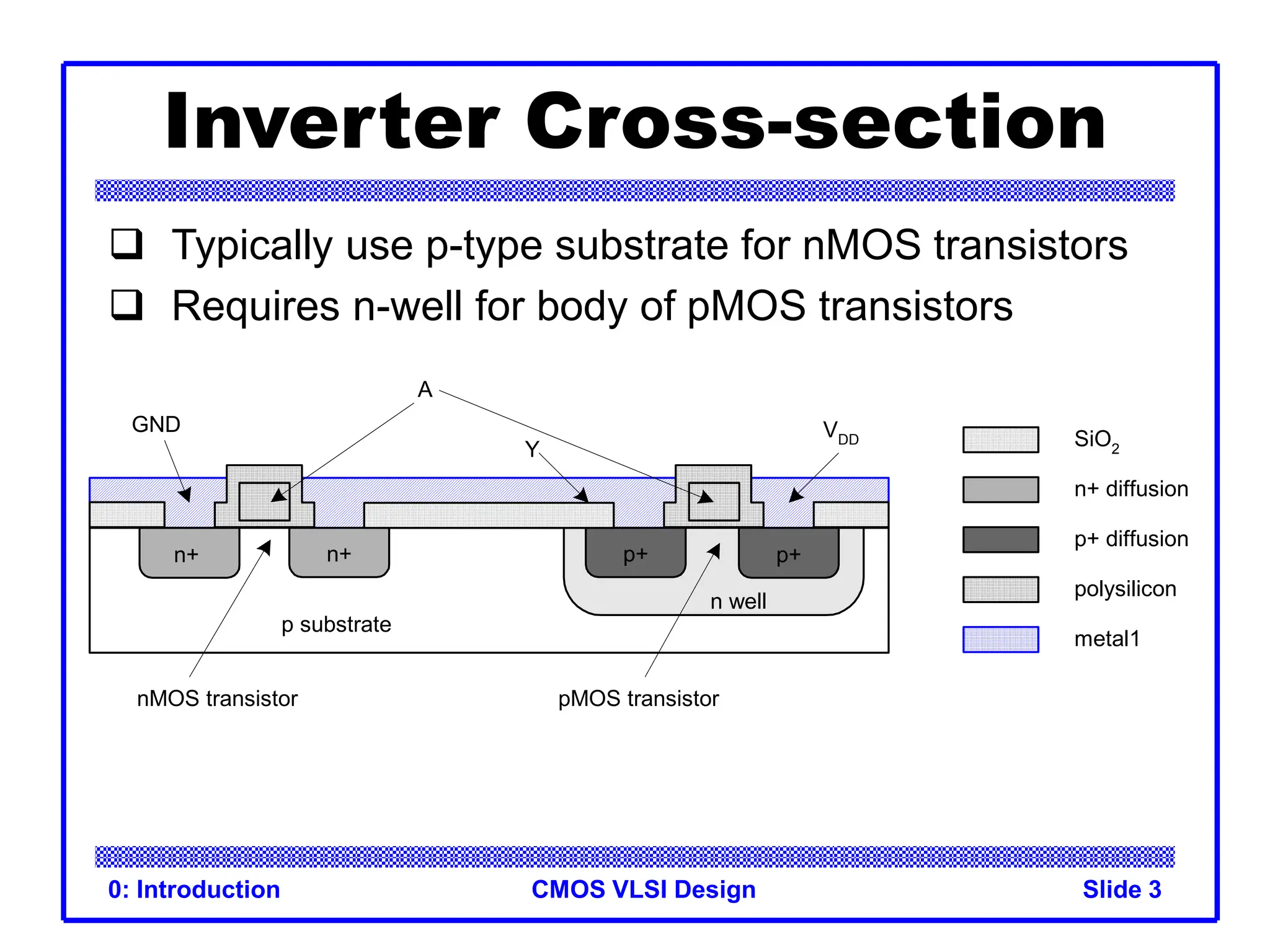
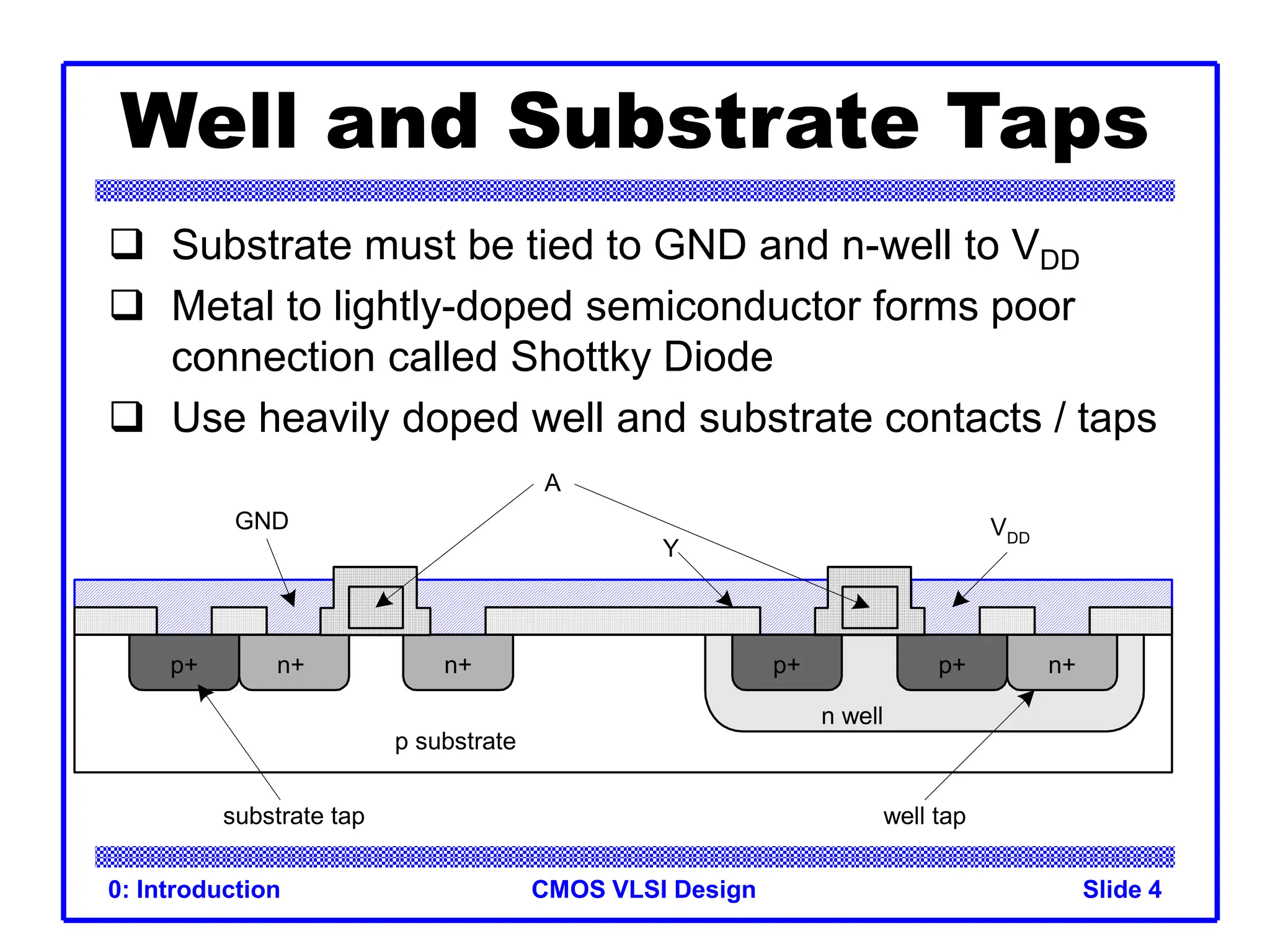
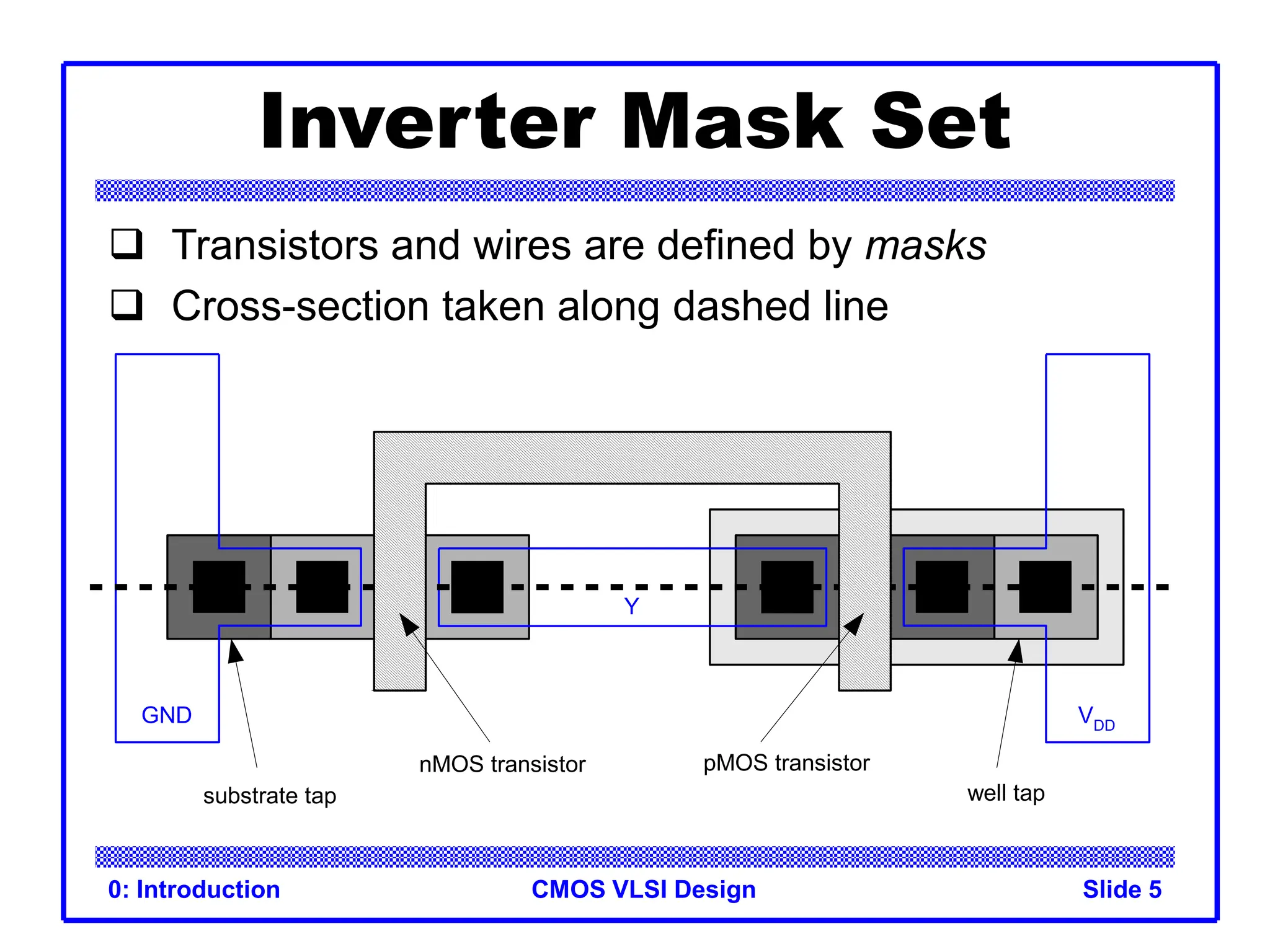
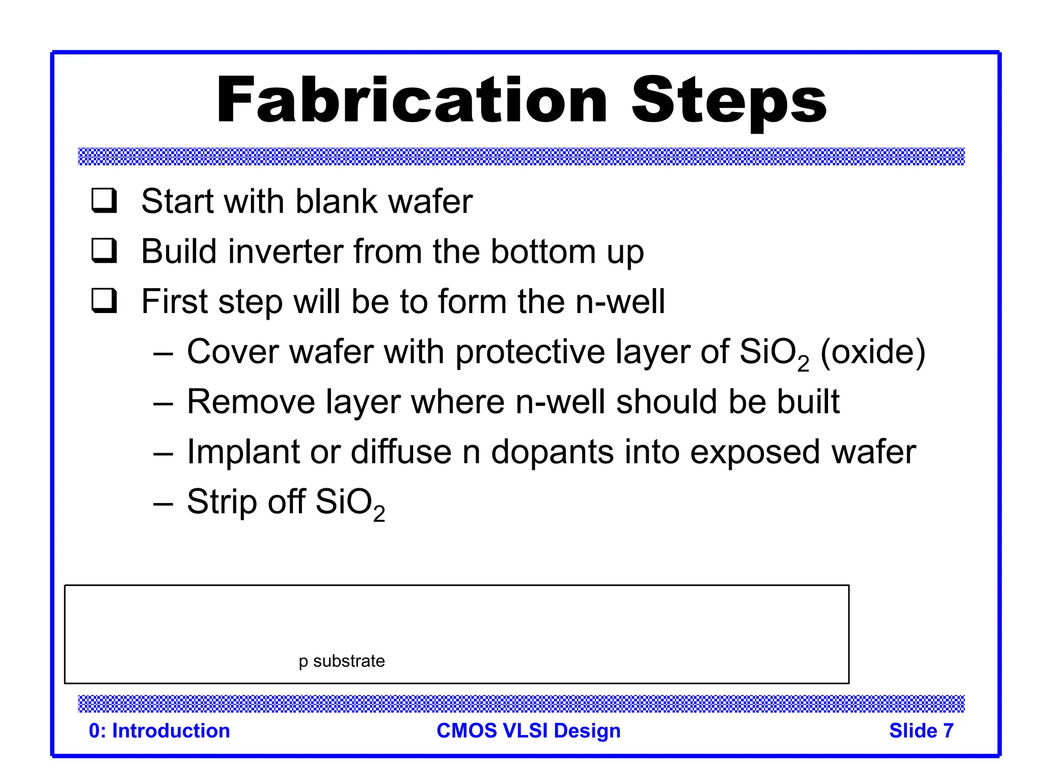
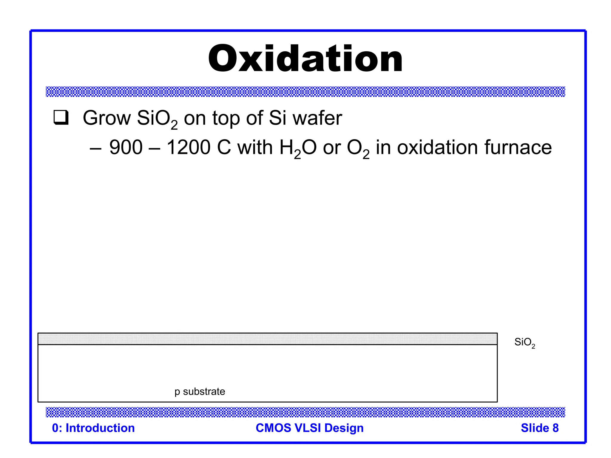
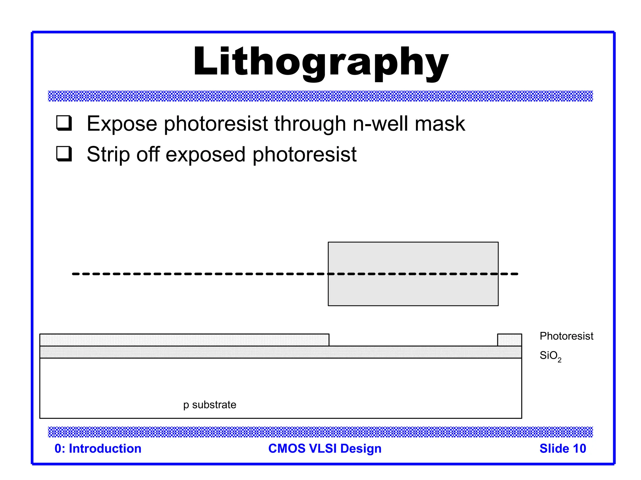
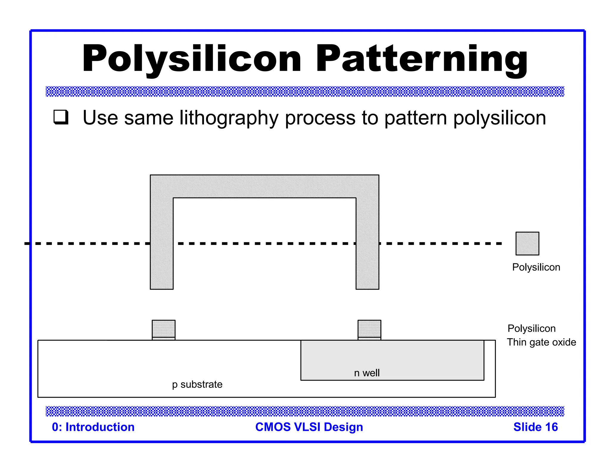
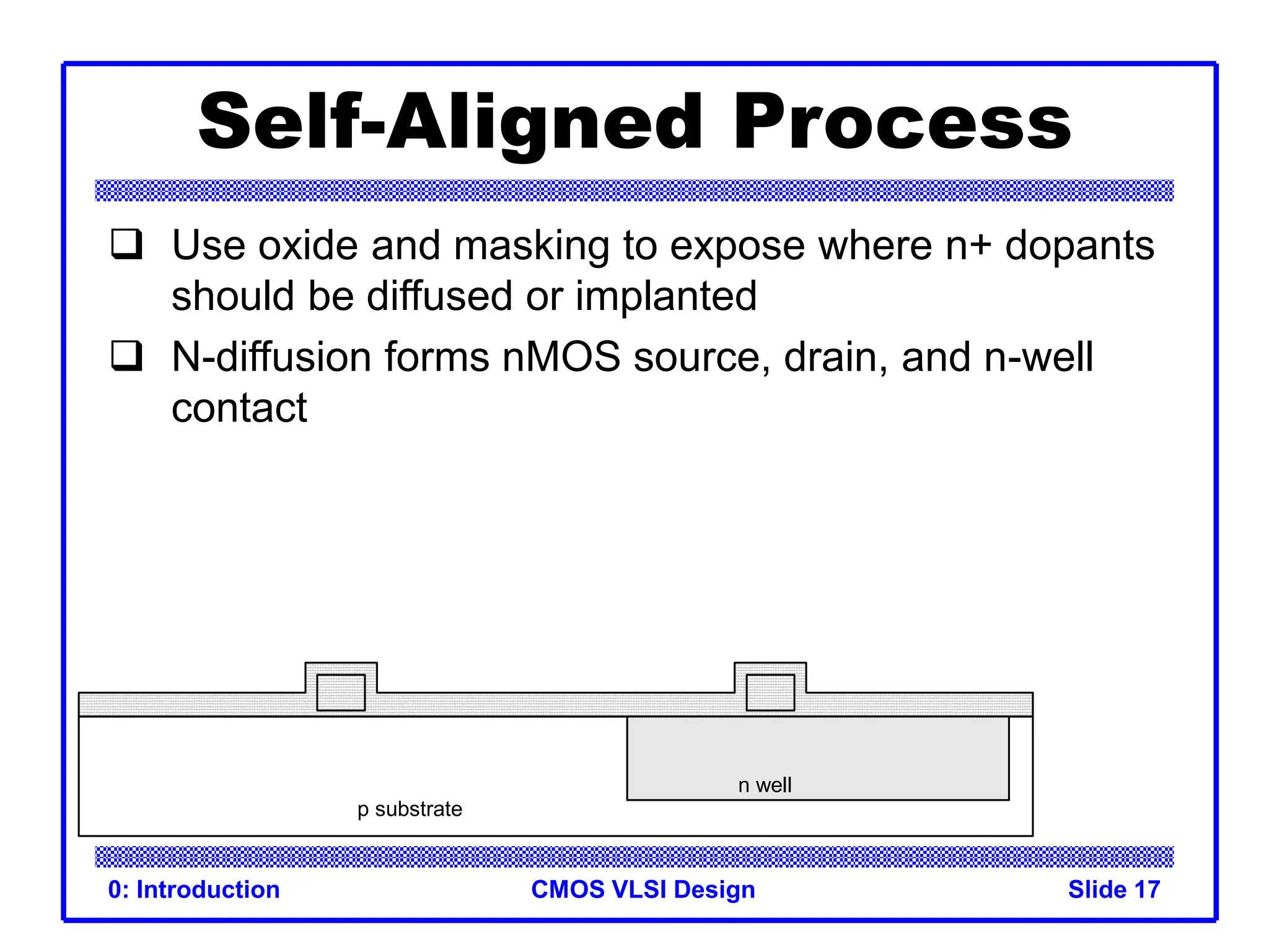
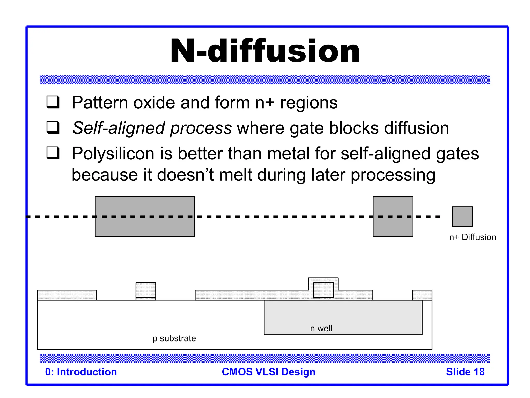
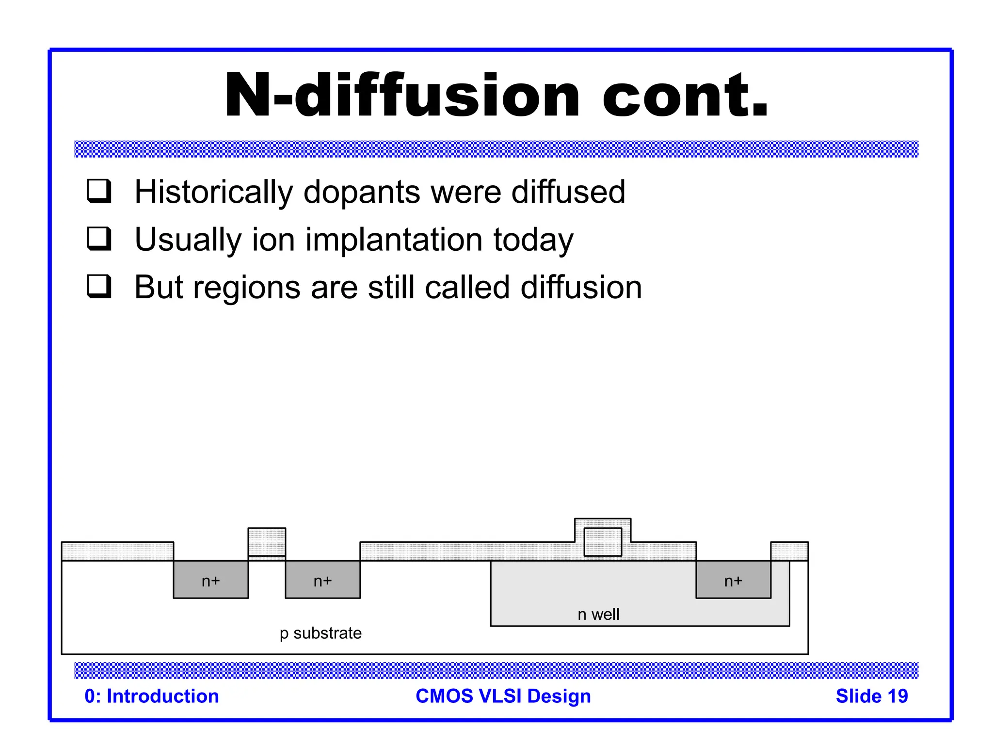
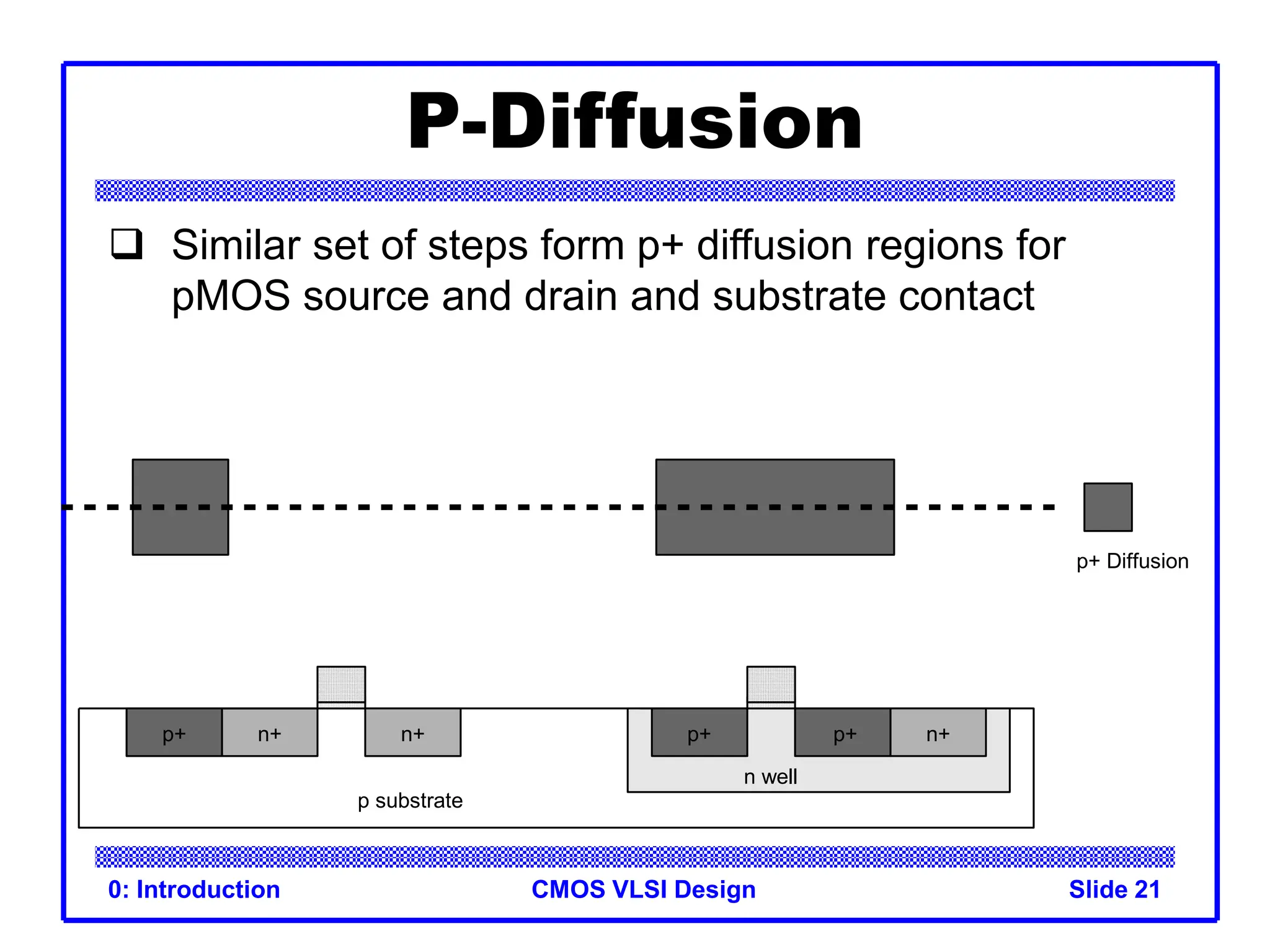
EE466: CMOS VLSI
Lecture 04: Fabrication
CMOS VLSI Design
0: Introduction Slide 2
CMOS Fabrication
 CMOS transistors are fabricated on silicon wafer
 Lithography process similar to printing press
 On each step, different materials are deposited or
etched
 Easiest to understand by viewing both top and
cross-section of wafer in a simplified manufacturing
process
CMOS VLSI Design
0: Introduction Slide 3
Inverter Cross-section
 Typically use p-type substrate for nMOS transistors
 Requires n-well for body of pMOS transistors
n+
p substrate
p+
n well
A
Y
GND VDD
n+ p+
SiO2
n+ diffusion
p+ diffusion
polysilicon
metal1
nMOS transistor pMOS transistor
CMOS VLSI Design
0: Introduction Slide 4
Well and Substrate Taps
 Substrate must be tied to GND and n-well to VDD
 Metal to lightly-doped semiconductor forms poor
connection called Shottky Diode
 Use heavily doped well and substrate contacts / taps
n+
p substrate
p+
n well
A
Y
GND VDD
n+
p+
substrate tap well tap
n+ p+
CMOS VLSI Design
0: Introduction Slide 5
Inverter Mask Set
 Transistors and wires are defined by masks
 Cross-section taken along dashed line
GND VDD
Y
A
substrate tap well tap
nMOS transistor pMOS transistor
CMOS VLSI Design
0: Introduction Slide 6
Detailed Mask Views
 Six masks
– n-well
– Polysilicon
– n+ diffusion
– p+ diffusion
– Contact
– Metal
Metal
Polysilicon
Contact
n+ Diffusion
p+ Diffusion
n well
CMOS VLSI Design
0: Introduction Slide 7
Fabrication Steps
 Start with blank wafer
 Build inverter from the bottom up
 First step will be to form the n-well
– Cover wafer with protective layer of SiO2 (oxide)
– Remove layer where n-well should be built
– Implant or diffuse n dopants into exposed wafer
– Strip off SiO2
p substrate
CMOS VLSI Design
0: Introduction Slide 8
Oxidation
 Grow SiO2 on top of Si wafer
– 900 – 1200 C with H2O or O2 in oxidation furnace
p substrate
SiO2
CMOS VLSI Design
0: Introduction Slide 9
Photoresist
 Spin on photoresist
– Photoresist is a light-sensitive organic polymer
– Softens where exposed to light
p substrate
SiO2
Photoresist
CMOS VLSI Design
0: Introduction Slide 10
Lithography
 Expose photoresist through n-well mask
 Strip off exposed photoresist
p substrate
SiO2
Photoresist
CMOS VLSI Design
0: Introduction Slide 11
Etch
 Etch oxide with hydrofluoric acid (HF)
– Seeps through skin and eats bone; nasty stuff!!!
 Only attacks oxide where resist has been exposed
p substrate
SiO2
Photoresist
CMOS VLSI Design
0: Introduction Slide 12
Strip Photoresist
 Strip off remaining photoresist
– Use mixture of acids called piranah etch
 Necessary so resist doesn’t melt in next step
p substrate
SiO2
CMOS VLSI Design
0: Introduction Slide 13
n-well
 n-well is formed with diffusion or ion implantation
 Diffusion
– Place wafer in furnace with arsenic gas
– Heat until As atoms diffuse into exposed Si
 Ion Implanatation
– Blast wafer with beam of As ions
– Ions blocked by SiO2, only enter exposed Si
n well
SiO2
CMOS VLSI Design
0: Introduction Slide 14
Strip Oxide
 Strip off the remaining oxide using HF
 Back to bare wafer with n-well
 Subsequent steps involve similar series of steps
p substrate
n well
CMOS VLSI Design
0: Introduction Slide 15
Polysilicon
 Deposit very thin layer of gate oxide
– < 20 Å (6-7 atomic layers)
 Chemical Vapor Deposition (CVD) of silicon layer
– Place wafer in furnace with Silane gas (SiH4)
– Forms many small crystals called polysilicon
– Heavily doped to be good conductor
Thin gate oxide
Polysilicon
p substrate
n well
CMOS VLSI Design
0: Introduction Slide 16
Polysilicon Patterning
 Use same lithography process to pattern polysilicon
Polysilicon
p substrate
Thin gate oxide
Polysilicon
n well
CMOS VLSI Design
0: Introduction Slide 17
Self-Aligned Process
 Use oxide and masking to expose where n+ dopants
should be diffused or implanted
 N-diffusion forms nMOS source, drain, and n-well
contact
p substrate
n well
CMOS VLSI Design
0: Introduction Slide 18
N-diffusion
 Pattern oxide and form n+ regions
 Self-aligned process where gate blocks diffusion
 Polysilicon is better than metal for self-aligned gates
because it doesn’t melt during later processing
p substrate
n well
n+ Diffusion
CMOS VLSI Design
0: Introduction Slide 19
N-diffusion cont.
 Historically dopants were diffused
 Usually ion implantation today
 But regions are still called diffusion
n well
p substrate
n+
n+ n+
CMOS VLSI Design
0: Introduction Slide 20
N-diffusion cont.
 Strip off oxide to complete patterning step
n well
p substrate
n+
n+ n+
CMOS VLSI Design
0: Introduction Slide 21
P-Diffusion
 Similar set of steps form p+ diffusion regions for
pMOS source and drain and substrate contact
p+ Diffusion
p substrate
n well
n+
n+ n+
p+
p+
p+
CMOS VLSI Design
0: Introduction Slide 22
Contacts
 Now we need to wire together the devices
 Cover chip with thick field oxide
 Etch oxide where contact cuts are needed
p substrate
Thick field oxide
n well
n+
n+ n+
p+
p+
p+
Contact
CMOS VLSI Design
0: Introduction Slide 23
Metalization
 Sputter on aluminum over whole wafer
 Pattern to remove excess metal, leaving wires
p substrate
Metal
Thick field oxide
n well
n+
n+ n+
p+
p+
p+
Metal
CMOS VLSI Design
0: Introduction Slide 24
Transistors as Switches
 We can view MOS transistors as electrically
controlled switches
 Voltage at gate controls path from source to drain
g
s
d
g = 0
s
d
g = 1
s
d
g
s
d
s
d
s
d
nMOS
pMOS
OFF
ON
ON
OFF
CMOS VLSI Design
0: Introduction Slide 25
CMOS Inverter
A Y
0
1
VDD
A Y
GND
A Y
CMOS VLSI Design
0: Introduction Slide 26
CMOS Inverter
A Y
0
1 0
VDD
A=1 Y=0
GND
ON
OFF
A Y
CMOS VLSI Design
0: Introduction Slide 27
CMOS Inverter
A Y
0 1
1 0
VDD
A=0 Y=1
GND
OFF
ON
A Y
CMOS VLSI Design
0: Introduction Slide 28
CMOS NAND Gate
A B Y
0 0
0 1
1 0
1 1
A
B
Y
CMOS VLSI Design
0: Introduction Slide 29
CMOS NAND Gate
A B Y
0 0 1
0 1
1 0
1 1
A=0
B=0
Y=1
OFF
ON ON
OFF
CMOS VLSI Design
0: Introduction Slide 30
CMOS NAND Gate
A B Y
0 0 1
0 1 1
1 0
1 1
A=0
B=1
Y=1
OFF
OFF ON
ON
CMOS VLSI Design
0: Introduction Slide 31
CMOS NAND Gate
A B Y
0 0 1
0 1 1
1 0 1
1 1
A=1
B=0
Y=1
ON
ON OFF
OFF
CMOS VLSI Design
0: Introduction Slide 32
CMOS NAND Gate
A B Y
0 0 1
0 1 1
1 0 1
1 1 0
A=1
B=1
Y=0
ON
OFF OFF
ON
CMOS VLSI Design
0: Introduction Slide 33
CMOS NOR Gate
A B Y
0 0 1
0 1 0
1 0 0
1 1 0
A
B
Y
CMOS VLSI Design
0: Introduction Slide 34
3-input NAND Gate
 Y pulls low if ALL inputs are 1
 Y pulls high if ANY input is 0
CMOS VLSI Design
0: Introduction Slide 35
3-input NAND Gate
 Y pulls low if ALL inputs are 1
 Y pulls high if ANY input is 0
A
B
Y
C
CMOS VLSI Design
0: Introduction Slide 36
Layout
 Chips are specified with set of masks
 Minimum dimensions of masks determine transistor
size (and hence speed, cost, and power)
 Feature size f = distance between source and drain
– Set by minimum width of polysilicon
 Feature size improves 30% every 3 years or so
 Normalize for feature size when describing design
rules
 Express rules in terms of l = f/2
– E.g. l = 0.3 mm in 0.6 mm process
CMOS VLSI Design
0: Introduction Slide 37
Simplified Design Rules
 Conservative rules to get you started
CMOS VLSI Design
0: Introduction Slide 38
Inverter Layout
 Transistor dimensions specified as Width / Length
– Minimum size is 4l / 2l, sometimes called 1 unit
– In f = 0.6 mm process, this is 1.2 mm wide, 0.6 mm
long
CMOS VLSI Design
0: Introduction Slide 39
Summary
 MOS Transistors are stack of gate, oxide, silicon
 Can be viewed as electrically controlled switches
 Build logic gates out of switches
 Draw masks to specify layout of transistors
 Now you know everything necessary to start
designing schematics and layout for a simple chip!

cmos-fabrication and nmos fabrication.ppt

  • 1.
    EE466: CMOS VLSI Lecture04: Fabrication
  • 2.
    CMOS VLSI Design 0:Introduction Slide 2 CMOS Fabrication  CMOS transistors are fabricated on silicon wafer  Lithography process similar to printing press  On each step, different materials are deposited or etched  Easiest to understand by viewing both top and cross-section of wafer in a simplified manufacturing process
  • 3.
    CMOS VLSI Design 0:Introduction Slide 3 Inverter Cross-section  Typically use p-type substrate for nMOS transistors  Requires n-well for body of pMOS transistors n+ p substrate p+ n well A Y GND VDD n+ p+ SiO2 n+ diffusion p+ diffusion polysilicon metal1 nMOS transistor pMOS transistor
  • 4.
    CMOS VLSI Design 0:Introduction Slide 4 Well and Substrate Taps  Substrate must be tied to GND and n-well to VDD  Metal to lightly-doped semiconductor forms poor connection called Shottky Diode  Use heavily doped well and substrate contacts / taps n+ p substrate p+ n well A Y GND VDD n+ p+ substrate tap well tap n+ p+
  • 5.
    CMOS VLSI Design 0:Introduction Slide 5 Inverter Mask Set  Transistors and wires are defined by masks  Cross-section taken along dashed line GND VDD Y A substrate tap well tap nMOS transistor pMOS transistor
  • 6.
    CMOS VLSI Design 0:Introduction Slide 6 Detailed Mask Views  Six masks – n-well – Polysilicon – n+ diffusion – p+ diffusion – Contact – Metal Metal Polysilicon Contact n+ Diffusion p+ Diffusion n well
  • 7.
    CMOS VLSI Design 0:Introduction Slide 7 Fabrication Steps  Start with blank wafer  Build inverter from the bottom up  First step will be to form the n-well – Cover wafer with protective layer of SiO2 (oxide) – Remove layer where n-well should be built – Implant or diffuse n dopants into exposed wafer – Strip off SiO2 p substrate
  • 8.
    CMOS VLSI Design 0:Introduction Slide 8 Oxidation  Grow SiO2 on top of Si wafer – 900 – 1200 C with H2O or O2 in oxidation furnace p substrate SiO2
  • 9.
    CMOS VLSI Design 0:Introduction Slide 9 Photoresist  Spin on photoresist – Photoresist is a light-sensitive organic polymer – Softens where exposed to light p substrate SiO2 Photoresist
  • 10.
    CMOS VLSI Design 0:Introduction Slide 10 Lithography  Expose photoresist through n-well mask  Strip off exposed photoresist p substrate SiO2 Photoresist
  • 11.
    CMOS VLSI Design 0:Introduction Slide 11 Etch  Etch oxide with hydrofluoric acid (HF) – Seeps through skin and eats bone; nasty stuff!!!  Only attacks oxide where resist has been exposed p substrate SiO2 Photoresist
  • 12.
    CMOS VLSI Design 0:Introduction Slide 12 Strip Photoresist  Strip off remaining photoresist – Use mixture of acids called piranah etch  Necessary so resist doesn’t melt in next step p substrate SiO2
  • 13.
    CMOS VLSI Design 0:Introduction Slide 13 n-well  n-well is formed with diffusion or ion implantation  Diffusion – Place wafer in furnace with arsenic gas – Heat until As atoms diffuse into exposed Si  Ion Implanatation – Blast wafer with beam of As ions – Ions blocked by SiO2, only enter exposed Si n well SiO2
  • 14.
    CMOS VLSI Design 0:Introduction Slide 14 Strip Oxide  Strip off the remaining oxide using HF  Back to bare wafer with n-well  Subsequent steps involve similar series of steps p substrate n well
  • 15.
    CMOS VLSI Design 0:Introduction Slide 15 Polysilicon  Deposit very thin layer of gate oxide – < 20 Å (6-7 atomic layers)  Chemical Vapor Deposition (CVD) of silicon layer – Place wafer in furnace with Silane gas (SiH4) – Forms many small crystals called polysilicon – Heavily doped to be good conductor Thin gate oxide Polysilicon p substrate n well
  • 16.
    CMOS VLSI Design 0:Introduction Slide 16 Polysilicon Patterning  Use same lithography process to pattern polysilicon Polysilicon p substrate Thin gate oxide Polysilicon n well
  • 17.
    CMOS VLSI Design 0:Introduction Slide 17 Self-Aligned Process  Use oxide and masking to expose where n+ dopants should be diffused or implanted  N-diffusion forms nMOS source, drain, and n-well contact p substrate n well
  • 18.
    CMOS VLSI Design 0:Introduction Slide 18 N-diffusion  Pattern oxide and form n+ regions  Self-aligned process where gate blocks diffusion  Polysilicon is better than metal for self-aligned gates because it doesn’t melt during later processing p substrate n well n+ Diffusion
  • 19.
    CMOS VLSI Design 0:Introduction Slide 19 N-diffusion cont.  Historically dopants were diffused  Usually ion implantation today  But regions are still called diffusion n well p substrate n+ n+ n+
  • 20.
    CMOS VLSI Design 0:Introduction Slide 20 N-diffusion cont.  Strip off oxide to complete patterning step n well p substrate n+ n+ n+
  • 21.
    CMOS VLSI Design 0:Introduction Slide 21 P-Diffusion  Similar set of steps form p+ diffusion regions for pMOS source and drain and substrate contact p+ Diffusion p substrate n well n+ n+ n+ p+ p+ p+
  • 22.
    CMOS VLSI Design 0:Introduction Slide 22 Contacts  Now we need to wire together the devices  Cover chip with thick field oxide  Etch oxide where contact cuts are needed p substrate Thick field oxide n well n+ n+ n+ p+ p+ p+ Contact
  • 23.
    CMOS VLSI Design 0:Introduction Slide 23 Metalization  Sputter on aluminum over whole wafer  Pattern to remove excess metal, leaving wires p substrate Metal Thick field oxide n well n+ n+ n+ p+ p+ p+ Metal
  • 24.
    CMOS VLSI Design 0:Introduction Slide 24 Transistors as Switches  We can view MOS transistors as electrically controlled switches  Voltage at gate controls path from source to drain g s d g = 0 s d g = 1 s d g s d s d s d nMOS pMOS OFF ON ON OFF
  • 25.
    CMOS VLSI Design 0:Introduction Slide 25 CMOS Inverter A Y 0 1 VDD A Y GND A Y
  • 26.
    CMOS VLSI Design 0:Introduction Slide 26 CMOS Inverter A Y 0 1 0 VDD A=1 Y=0 GND ON OFF A Y
  • 27.
    CMOS VLSI Design 0:Introduction Slide 27 CMOS Inverter A Y 0 1 1 0 VDD A=0 Y=1 GND OFF ON A Y
  • 28.
    CMOS VLSI Design 0:Introduction Slide 28 CMOS NAND Gate A B Y 0 0 0 1 1 0 1 1 A B Y
  • 29.
    CMOS VLSI Design 0:Introduction Slide 29 CMOS NAND Gate A B Y 0 0 1 0 1 1 0 1 1 A=0 B=0 Y=1 OFF ON ON OFF
  • 30.
    CMOS VLSI Design 0:Introduction Slide 30 CMOS NAND Gate A B Y 0 0 1 0 1 1 1 0 1 1 A=0 B=1 Y=1 OFF OFF ON ON
  • 31.
    CMOS VLSI Design 0:Introduction Slide 31 CMOS NAND Gate A B Y 0 0 1 0 1 1 1 0 1 1 1 A=1 B=0 Y=1 ON ON OFF OFF
  • 32.
    CMOS VLSI Design 0:Introduction Slide 32 CMOS NAND Gate A B Y 0 0 1 0 1 1 1 0 1 1 1 0 A=1 B=1 Y=0 ON OFF OFF ON
  • 33.
    CMOS VLSI Design 0:Introduction Slide 33 CMOS NOR Gate A B Y 0 0 1 0 1 0 1 0 0 1 1 0 A B Y
  • 34.
    CMOS VLSI Design 0:Introduction Slide 34 3-input NAND Gate  Y pulls low if ALL inputs are 1  Y pulls high if ANY input is 0
  • 35.
    CMOS VLSI Design 0:Introduction Slide 35 3-input NAND Gate  Y pulls low if ALL inputs are 1  Y pulls high if ANY input is 0 A B Y C
  • 36.
    CMOS VLSI Design 0:Introduction Slide 36 Layout  Chips are specified with set of masks  Minimum dimensions of masks determine transistor size (and hence speed, cost, and power)  Feature size f = distance between source and drain – Set by minimum width of polysilicon  Feature size improves 30% every 3 years or so  Normalize for feature size when describing design rules  Express rules in terms of l = f/2 – E.g. l = 0.3 mm in 0.6 mm process
  • 37.
    CMOS VLSI Design 0:Introduction Slide 37 Simplified Design Rules  Conservative rules to get you started
  • 38.
    CMOS VLSI Design 0:Introduction Slide 38 Inverter Layout  Transistor dimensions specified as Width / Length – Minimum size is 4l / 2l, sometimes called 1 unit – In f = 0.6 mm process, this is 1.2 mm wide, 0.6 mm long
  • 39.
    CMOS VLSI Design 0:Introduction Slide 39 Summary  MOS Transistors are stack of gate, oxide, silicon  Can be viewed as electrically controlled switches  Build logic gates out of switches  Draw masks to specify layout of transistors  Now you know everything necessary to start designing schematics and layout for a simple chip!