Downloaded 442 times

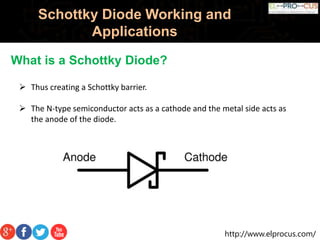

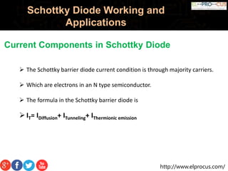


The document discusses the working, construction, characteristics, and applications of Schottky diodes, which are low voltage electronic components known for their fast switching speed and efficiency. It explains the formation of a Schottky barrier through a metal-semiconductor junction and highlights their advantages over traditional diodes, including lower forward voltage drop and quick recovery times. Schottky diodes are commonly used in applications requiring voltage clamping, rectification in power supplies, and high-speed switching.