Downloaded 2,827 times

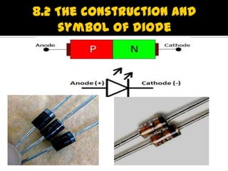
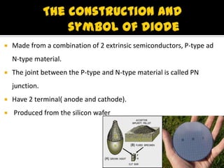


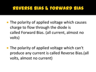


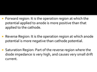


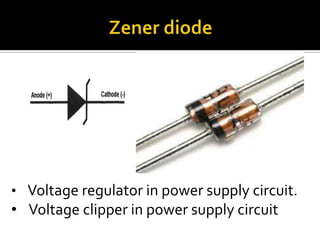


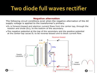


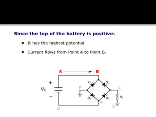


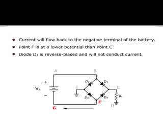
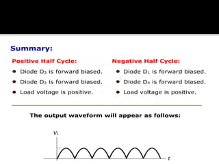


The document discusses diodes, including their history and components. It describes how a diode is constructed from a P-type and N-type semiconductor material, forming a PN junction. At the junction, electrons diffuse into holes, creating a depletion region that acts as an insulator under reverse bias but allows current to flow under forward bias. The document outlines diode applications such as rectification in power supplies and their characteristic I-V curve.