
Recommended
More Related Content
Similar to silicon on insulator types and its characterstics
Similar to silicon on insulator types and its characterstics (20)
More from SIVA NAGI REDY KALLI
Recently uploaded
Recently uploaded (20)
silicon on insulator types and its characterstics
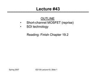
- 1. Spring 2007 EE130 Lecture 43, Slide 1 Lecture #43 OUTLINE • Short-channel MOSFET (reprise) • SOI technology Reading: Finish Chapter 19.2
- 2. Spring 2007 EE130 Lecture 43, Slide 2 Short-Channel MOSFET • IDS does not saturate with increasing VDS due to DIBL, and also channel-length modulation for VDS>VGS-VT 0 1 2 2.5 Vds (V) 0.0 0.1 0.2 0.3 0.4 I ds (mA/m) L = 0.15 m Vgs = 2.5V Vgs = 2.0V Vgs = 1.5V Vgs = 1.0V ) L = 2.0 m Vgs = 2.5V 0.02 0.03 Vt = 0.7 V Vt = 0.4 V OUTPUT CHARACTERISTICS TRANSFER CHARACTERISTICS
- 3. Spring 2007 EE130 Lecture 43, Slide 3 Silicon on Insulator (SOI) Technology • Transistors are fabricated in a thin single-crystal Si layer on top of an electrically insulating layer of SiO2 Simpler device isolation savings in circuit layout area Low junction capacitances faster circuit operation Better soft-error immunity No body effect Higher cost TSOI
- 4. Spring 2007 EE130 Lecture 43, Slide 4 Partially Depleted SOI (PD-SOI) Floating body effect (history dependent): 1. When a PD-SOI NMOSFET is in the ON state, at moderate-to-high VDS, holes are generated via impact ionization near the drain 2. Holes are swept into the neutral body, collecting at the source junction 3. The body-source pn junction is forward biased 4. VT is lowered IDsat increases “kink” in output ID vs. VDS curve body F s T T SOI qN W W T ) 2 ( 2 where ,
- 5. Spring 2007 EE130 Lecture 43, Slide 5 Fully Depleted SOI (FD-SOI) • No floating body effect! • VT is sensitive to SOI film thickness • Poorer control of short-channel effects due to fringing electric field from drain • Elevated S/D contact structure needed to reduce RS, RD body F s T T SOI qN W W T ) 2 ( 2 where , Silicon Substrate Source Drain SiO2 SOI Gate