Clamping Circuit and Clipping Circuit, Principle of Operation of Clamping Circuit, Biased positive clamping circuit, Biased negative clamping circuit, Classification of Clipping Circuit, Clipping Circuit, Zener Diode as a Peak Clipper, Application of Clipper.
,
The three terminals of the FET are known as Gate, Drain, and Source.
It is a voltage controlled device, where the input voltage controls by the output current.
In FET current used to flow between the drain and the source terminal. And this current can be controlled by applying the voltage between the gate and the source terminal.
So this applied voltage generate the electric field within the device and by controlling these electric field we can control the flow of current through the device.
This ppt provides a brief overview on thyristors commonly known as SCRs. V- I characteristics curve, triggering methods, protection methods, series and parallel operations of SCRs, applications are discussed in this slide.
Do Diodes and electronic stuff freaks you out?And what about those clippers and clampers?The details are as follows.
You can learn every concept related to it here.Enjoy clipping :)
PN junction diode –structure, operation and V-I characteristics, diffusion and transient capacitance - Rectifiers – Half Wave and Full Wave Rectifier,– Display devices- LED, Laser diodes- Zener diodecharacteristics-Zener Reverse characteristics – Zener as regulator,TRANSISTORS, BJT, JFET, MOSFET- structure, operation, characteristics and Biasing UJT, Thyristor and IGBT Structure and characteristics,BJT small signal model – Analysis of CE, CB, CC amplifiers- Gain and frequency response –
MOSFET small signal model– Analysis of CS and Source follower – Gain and frequency response- High frequency analysis,BIMOS cascade amplifier, Differential amplifier – Common mode and Difference mode analysis – FET input stages – Single tuned amplifiers – Gain and frequency response – Neutralization methods, power amplifiers –Types (Qualitative analysis),Advantages of negative feedback – voltage / current, series , Shunt feedback –positive feedback – Condition for oscillations, phase shift – Wien bridge, Hartley, Colpitts and Crystal oscillators.
It’s a power electronics project. It is able to give output voltage(DC) more and less than input voltage as per requirement.
We can generate variable DC voltage which is less than input, but, the special things about this converter is, it has capability to produce variable DC voltage as high as twice the input voltage.
We have specially designed and manufactured inductor for this project.
Semiconductor
If a valence Electron acquires sufficient kinetic energy to break its covalent bond and fills the void created by a hole then a vacancy, or hole will be created in the covalent bond that released the electron
Hence there is a transfer of holes to the left and electrons to the right
Diodes and its application encapsulate the different characteristics of different type of diodes. Also, define its different biases and how it works.
It provides shortcut method in analyzing Clamper and clipper.
At the end of the powerpoint, there has a review question to answer with answer key provided.
International Refereed Journal of Engineering and Science (IRJES)irjes
International Refereed Journal of Engineering and Science (IRJES) is a leading international journal for publication of new ideas, the state of the art research results and fundamental advances in all aspects of Engineering and Science. IRJES is a open access, peer reviewed international journal with a primary objective to provide the academic community and industry for the submission of half of original research and applications.
Pre Final Year project/ mini project for Electronics and communication engine...Shirshendu Das
Mini project for Electronics and communication engineering (ECE) to build an AC to DC power supply using Full Wave Rectifier having input as 220-240V AC and giving stable filtered output of 5V, -5V & variable 5V DC. Simulation of the circuit was done in Proteus design suite.
The three types of rectifiers in just 18 slides. Learn and enjoy the concepts. This PowerPoint presentation not only tells about the working and principles of rectifiers but also determines the disadvantages and advantages of different rectifiers. This PowerPoint presentation also has circuit diagrams that suit your necessities. This PPT can be written as an answer for a long type of question too.
Electrical Drives and Control Heating and Cooling CurvesDr.Raja R
Electrical Drives and Control
Heating and Cooling Curves
Relation Ship Between Temperature Rise and Time:
Heating time constant
Cooling time constant
MUTHAYAMMAL ENGINEERING COLLEGE
Electric Drives and Controls Unit 1 IntroductionDr.Raja R
Electric Drives and Controls
Unit 1 Introduction
Block Diagram of Electric Drive
Power Source
Power Modulator
Load
Control Unit
Sensing Unit
Motor
Classification of Electrical Drives
Advantages of Electrical Drives
Disadvantages of Electrical Drive
Applications of Electrical Drives
Environmental impacts of renewable energy generation systems (cost ghg emission)Dr.Raja R
Environmental Impacts of Renewable Energy Generation Systems (Cost-GHG Emission)
Power Electronics for Renewable Energy Systems
Renewable Energy Systems
Solar
Wind
Ocean
Hydro
Applications of carbon materials in electrical engineeringDr.Raja R
Applications of carbon materials in electrical engineering
Introduction
Carbon Use for Making Filament of Incandescent Lamp
Carbon Use for Making Electrical Contacts
Carbon Use for Making Resistors
Carbon Use for Making Brushes for Electrical DC Machines and Alternators
Carbon Use for Making Dry Cell Elements
Carbon Electrodes Use for Electric Furnaces
Graphite Carbon Use for Arc Lighting and Welding Electrodes
Carbon use as Component of Vacuum Valves and Tubes
High Voltage Transformers
Voltage Regulation, Variation of Alternator Field Current, Voltage Regulation by Inserting Resistance or Inductance, Induction Regulator Method,Voltage Variation by Means of Tapped Transformer
Making india non fossil fuel based, Types of Renewable Energy Sources, Solar Energy
Wind Energy
Hydro Energy
Tidal Energy
Geothermal Energy and
Biomass Energy
Rooftop Solar - Future for India, Grid-Connected and Off-Grid Rooftop Solar System, Hybrid Systems, CAPEX Model (Capital Expenditure Model), OPEX Model (Operating Expenses Model), Inside the Home of the Future
Introduction to reactive power control in electrical powerDr.Raja R
Introduction to reactive power control in electrical power
Reactive power in transmission line :
Reactive power control
Reactive power and its importance
Apparent Power
Reactive Power
Apparent Power
Reactive Power Formula
Basic Difference Between Wires and CablesDr.Raja R
Basic Difference Between Wires and Cables
What’s the basic difference between Wires and Cables?
List some of the basic differences between Wires and Cables
Different uses of Wire and Cable
Types of Wire and Cable
Different advantages of using Wire and Cable
NAAC (Criterion-I : Curricular Aspects for Autonomous Engineering Colleges)Dr.Raja R
NAAC (Criterion-I : Curricular Aspects for Autonomous Engineering Colleges),
Introduction
Key Indicators (KIs)
1.1 Curriculum Design and Development
1.2 Academic Flexibility
1.3 Curriculum Enrichment
1.4 Feedback System
List of Files and Documents Required
Data Templates/Documents - Quantitative Metrics (QnM)
Low power architecture of logic gates using adiabatic techniquesnooriasukmaningtyas
The growing significance of portable systems to limit power consumption in ultra-large-scale-integration chips of very high density, has recently led to rapid and inventive progresses in low-power design. The most effective technique is adiabatic logic circuit design in energy-efficient hardware. This paper presents two adiabatic approaches for the design of low power circuits, modified positive feedback adiabatic logic (modified PFAL) and the other is direct current diode based positive feedback adiabatic logic (DC-DB PFAL). Logic gates are the preliminary components in any digital circuit design. By improving the performance of basic gates, one can improvise the whole system performance. In this paper proposed circuit design of the low power architecture of OR/NOR, AND/NAND, and XOR/XNOR gates are presented using the said approaches and their results are analyzed for powerdissipation, delay, power-delay-product and rise time and compared with the other adiabatic techniques along with the conventional complementary metal oxide semiconductor (CMOS) designs reported in the literature. It has been found that the designs with DC-DB PFAL technique outperform with the percentage improvement of 65% for NOR gate and 7% for NAND gate and 34% for XNOR gate over the modified PFAL techniques at 10 MHz respectively.
6th International Conference on Machine Learning & Applications (CMLA 2024)ClaraZara1
6th International Conference on Machine Learning & Applications (CMLA 2024) will provide an excellent international forum for sharing knowledge and results in theory, methodology and applications of on Machine Learning & Applications.
Literature Review Basics and Understanding Reference Management.pptxDr Ramhari Poudyal
Three-day training on academic research focuses on analytical tools at United Technical College, supported by the University Grant Commission, Nepal. 24-26 May 2024
Hierarchical Digital Twin of a Naval Power SystemKerry Sado
A hierarchical digital twin of a Naval DC power system has been developed and experimentally verified. Similar to other state-of-the-art digital twins, this technology creates a digital replica of the physical system executed in real-time or faster, which can modify hardware controls. However, its advantage stems from distributing computational efforts by utilizing a hierarchical structure composed of lower-level digital twin blocks and a higher-level system digital twin. Each digital twin block is associated with a physical subsystem of the hardware and communicates with a singular system digital twin, which creates a system-level response. By extracting information from each level of the hierarchy, power system controls of the hardware were reconfigured autonomously. This hierarchical digital twin development offers several advantages over other digital twins, particularly in the field of naval power systems. The hierarchical structure allows for greater computational efficiency and scalability while the ability to autonomously reconfigure hardware controls offers increased flexibility and responsiveness. The hierarchical decomposition and models utilized were well aligned with the physical twin, as indicated by the maximum deviations between the developed digital twin hierarchy and the hardware.
Using recycled concrete aggregates (RCA) for pavements is crucial to achieving sustainability. Implementing RCA for new pavement can minimize carbon footprint, conserve natural resources, reduce harmful emissions, and lower life cycle costs. Compared to natural aggregate (NA), RCA pavement has fewer comprehensive studies and sustainability assessments.
A review on techniques and modelling methodologies used for checking electrom...nooriasukmaningtyas
The proper function of the integrated circuit (IC) in an inhibiting electromagnetic environment has always been a serious concern throughout the decades of revolution in the world of electronics, from disjunct devices to today’s integrated circuit technology, where billions of transistors are combined on a single chip. The automotive industry and smart vehicles in particular, are confronting design issues such as being prone to electromagnetic interference (EMI). Electronic control devices calculate incorrect outputs because of EMI and sensors give misleading values which can prove fatal in case of automotives. In this paper, the authors have non exhaustively tried to review research work concerned with the investigation of EMI in ICs and prediction of this EMI using various modelling methodologies and measurement setups.
A review on techniques and modelling methodologies used for checking electrom...
Clamping Circuit and Clipping Circuit
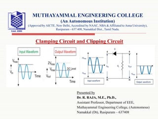
1. Presented by
Dr. R. RAJA, M.E., Ph.D.,
Assistant Professor, Department of EEE,
Muthayammal Engineering College, (Autonomous)
Namakkal (Dt), Rasipuram – 637408
MUTHAYAMMAL ENGINEERING COLLEGE
(An Autonomous Institution)
(Approved by AICTE, New Delhi, Accredited by NAAC, NBA & Affiliated to Anna University),
Rasipuram - 637 408, Namakkal Dist., Tamil Nadu.
Clamping Circuit and Clipping Circuit
2. Clamping Circuit
The circuit which can set the positive or negative peak of the input AC signal at a
required level is what we call as a clamping circuit. This circuit quickly adds or
subtracts a DC element to the input AC signal. Other than the name clamping
circuit, Baseline Stabilizer or DC Reinserted or Level Shifter or D.C Restorer are
also frequently used.
The requirement of clamper circuit is similar to in TV receivers; where the
signal moves through the capacitive coupling network, then the dc component
of these signal will get lost. This DC component (not exactly same as that of the
lost one) will get restored using this clamping circuit. This circuit will add the
DC element which will be positive or negative to the AC input signal. It pushes
the signal towards the positive or the negative side (shown below). Here; when
it shifts the signal to upward side or positive side, both negative peak and the
zero level will meet which is called positive clamper circuit.
10/23/2020 2
3. Contd..
When it shifts the signal to the downside or negative side, both positive peak
and the zero level will meet which we refer as the negative clamper circuit.
10/23/2020 3
4. Contd..
The minimum number of components of a clamping circuit is three – a capacitor,
a resistor and a diode. In some cases, DC supply is also needed to give an
additional shift. The nature of the waveform remains alike, but the difference is in
the shifted level. The peak to peak value of the waveform will never change.
The peak value and average value of the input waveform and the clamped output
will be different. The time constant of the circuit (RC) must have to be ten times
the time-period of the entering (input) AC voltage for better clamping action.
Now, we can assume a negative clamper shown in figure 2. Throughout the
positive half cycle of input, the D diode will conduct, and the output voltage will
be same as barrier potential of the diode (V0). At that time, the capacitor will get
charged to (V – V0). Throughout the negative half cycle of input, the diode will
become negative biased, and it has no role on capacitor voltage. The capacitor
cannot discharge a lot because of the high value of R. Therefore output voltage
will be – (2V- V0). The peak to peak voltage will be 2V. The output waveform that
we get will be the original signal shifted in the downward direction.
10/23/2020 4
5. Contd..
10/23/2020 5
Next, we can assume a positive clamper shown in figure 3. The one and only
distinction from the previous circuit is that diode is in reverse polarity. So the output
will be the shifted original signal in the upward direction.
6. Contd..
The explanation and working are same as above clamper circuit. Thus we can
conclude that we obtain the positive clamper if the diode in the circuit points
the upward direction and we get negative clamperwhen the diode points in the
downward direction.
10/23/2020 6
7. Contd..
Principle of Operation of Clamping Circuit
In general, the clamper circuit depends on a variation in the capacitor time constant
The time constant should be sufficient that the capacitor voltage does not discharge
considerably throughout the non-conducting diode period. One should select the
values of capacitance and resistance in such a way that the circuit keeps the time
constant high. For preventing quick the discharge of capacitor, the resistance value
should be high. All through the diode conducting period, the capacitor charging
should be very fast. For this, we select a small value of capacitance.
The C in the positive clamper charges quickly throughout the first negative phase of
AC input voltage. When Vin becomes +ve, the C serves as a voltage doubler and
when Vin is –ve, the C operates as a battery with voltage Vin. Thus, we can conclude
that the capacitor and input voltage act against each other. This results in zero net
voltage as seen by the load.
10/23/2020 7
10. Classification of Clipping Circuit
According to non linear devices used
- Diode Clippers.
- Transistor Clippers.
According to biasing
- Unbiased Clippers.
- Biased Clippers.
According to configuration used
- Series diode clippers.
- Shunt or Parallel diode clippers.
- A series combination of reference supply, resistor and diode.
- Multi-diode clippers comprises of a number of diodes, resistors and
reference voltage.
- Two emitter-coupled transistors functioning as an over driven difference
amplifier.
10/23/2020 10
11. Classification of Clipping Circuit
According to non linear devices used
- Diode Clippers.
- Transistor Clippers.
According to biasing
- Unbiased Clippers.
- Biased Clippers.
According to configuration used
- Series diode clippers.
- Shunt or Parallel diode clippers.
- A series combination of reference supply, resistor and diode.
- Multi-diode clippers comprises of a number of diodes, resistors and
reference voltage.
- Two emitter-coupled transistors functioning as an over driven difference
amplifier.
.
10/23/2020 11
12. Clipping Circuit
It is in fact a wave shaping circuit, which can control the shape of the output
waveform by eliminating or clipping a part of applied wave. This is done
without distorting the other (remaining) part of waveform.
The clipping circuit does not have energy storage elements (capacitors) but it
includes both linear (Resistors) and nonlinear elements (transistors or junction
diodes). This circuit is normally used for the selection in the transmission
purpose.
In transmission, a portion of a signal wave form occupied below or above a
particular reference voltage level is selected. Other than the name – Clipping
circuits; Slicers, Clippers, Limiters or Amplitude selectors are also often used.
10/23/2020 12
13. Contd..
Diode Clippers
At least two components – an ideal diode and resistor are employed for the
formation of these clippers. In some cases; for fixing the clipping level, a DC
battery is also used (Figure 1). When the circuit is forward biased, the ideal
diode used operates as a closed switch.
When the circuit is reversed biased, the ideal diode used operates as an open
switch. Here; by altering the voltage of the battery and by exchanging the
position of the various elements, the input waveform can be clipped.
10/23/2020 13
14. Contd..
Positive clippers
It actually removes the positive half cycles of the input voltage. Here in positive
series clipper, when the input is positive then the diode is in reverse biased condition
(output is zero) and when the input is negative, then the diode is in forward biased
condition (figure 2)
10/23/2020 14
15. Contd..
In positive shunt clipper, when the input is negative, the whole input voltage appears
across the resistor RL or diode (if R<L). When R<L, this circuit will operates as
voltage divider and its output voltage is
10/23/2020 15
16. Contd..
When the diode is connected in reverse polarity in the circuits of positive series
clipper and positive shunt clipper, it becomes negative series clipper and negative
shunt clipper respectively (figures 4 and 5). These clippers can eliminate the entire
negative half cycle of input voltage.
10/23/2020 16
17. Contd..
10/23/2020 17
The clippers discussed above are considered as the circuits with ideal diode. But if
the barrier potential (V0) is considered (Si = 0.7 V and Ge = 0.3 V), the output
voltage of positive and negative clippers are shown below.
18. Contd..
10/23/2020 18
Biased Clippers
In some cases, we need to eliminate a tiny portion of positive or negative half cycles of
the input signal voltage. In that case we use biased clippers.
While during the negative half cycle of input signal in biased negative clipper circuit, it
removes the input signal voltage when it is greater than the battery voltage. When the
battery and diode is reversed, the clipping can be changed to biased positive clipper
(Figure 7).
20. Contd..
Combination Clipper
For removing a portion of both positive and negative half cycle of input signal,
we use this combination clipper (figure below).
10/23/2020 20
21. Contd..
Zener Diode as a Peak Clipper
Zener diodes can be employed for removing (clipping off) the portion of input
waveform in the wave shaping circuit (see figure below).
10/23/2020 21
22. Contd..
Application of Clipper
TV Transmitters and Receivers.
Noise Limiters.
Protection of different circuits.
Different wave generation.
10/23/2020 22