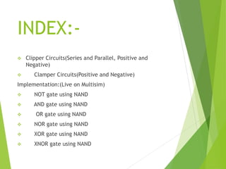
The document is a presentation slide deck on clippers, clampers, and realizing logic gates using NAND gates only. Some key points:
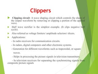
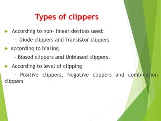
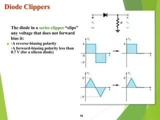
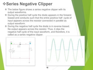
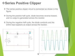
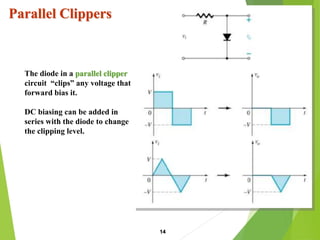
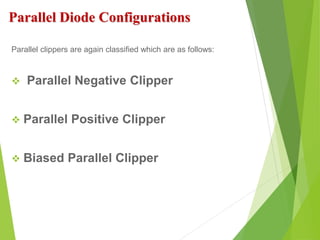
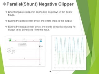
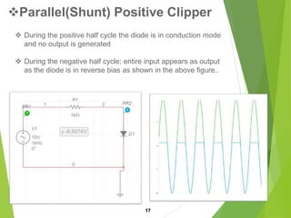
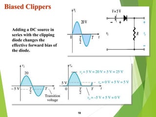
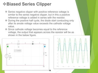
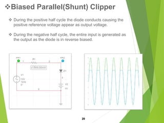
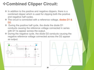
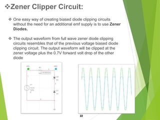
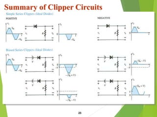
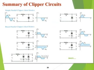
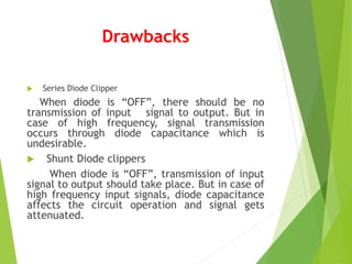
- It describes different types of clipper circuits including series, parallel, positive, negative, and biased clippers. It also explains how clippers work to clip portions of input waveforms.
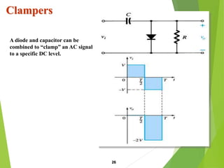
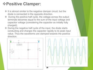
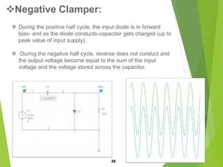
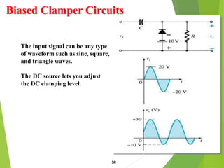
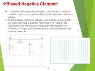
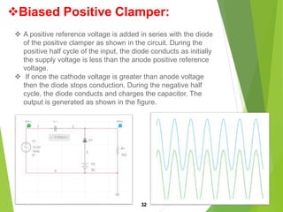
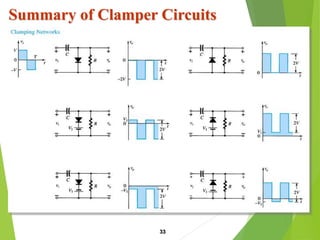
- It covers different types of clamper circuits including positive, negative, and biased clampers. It explains how clampers work to clamp output waveforms to a fixed DC level.
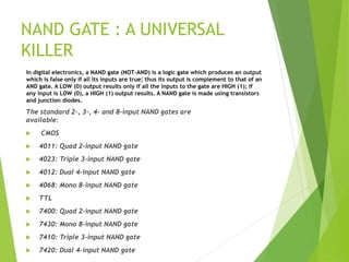
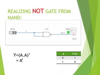
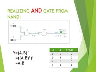
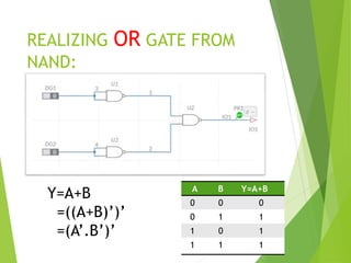
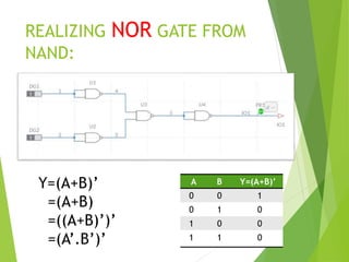
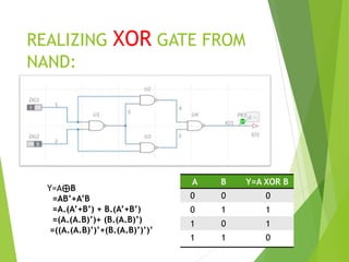
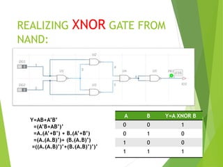
- It demonstrates how to realize all basic logic gates (NOT, AND, OR, NOR, XOR, XNOR) using only NAND gates as the universal logic gate. Truth tables and
Bipolar junction transistors (BJTs) are three-terminal semiconductor devices consisting of two pn junctions. There are two types, NPN and PNP, depending on the order of doping. BJTs can operate as amplifiers and switches by controlling the flow of majority charge carriers through the base terminal. Proper biasing is required to operate the transistor in its active region between cutoff and saturation. Common configurations include common-base, common-emitter, and common-collector, each with different input and output characteristics. Maximum ratings like power dissipation and voltages must be considered for circuit design and temperature derating.
This document discusses digital to analog converters (DACs). It explains that a DAC converts digital numbers into analog voltages or currents. The key components of a DAC are its digital input, analog output, and conversion process. Common DAC types include binary weighted resistor DACs and R-2R ladder DACs, which use resistors and switches to implement the conversion. Important DAC specifications are also outlined such as reference voltage, resolution, speed, settling time, and linearity. Common applications of DACs include function generators, digital oscilloscopes, and converting digital video signals to analog formats for display.
This document discusses different types of avalanche transit time devices (ATTDs) used to generate microwaves, including IMPATT diodes and TRAPATT diodes. It provides details on:
1) The basics of how ATTDs like IMPATT and TRAPATT diodes utilize the avalanche breakdown effect across a reverse-biased p-n junction to produce carriers and negative resistance at microwave frequencies.
2) The different modes of ATTD oscillators, including the IMPATT mode where typical efficiency is 5-10% and frequencies can reach 100 GHz, and the TRAPATT mode with higher typical efficiency of 20-60%.
3) The physical structures and operating principles of IMPATT diodes
This document discusses op-amp clipper circuits. It begins by introducing op-amps and their applications. It then defines a clipper as a circuit that prevents an output from exceeding a voltage level without distorting the waveform. The document discusses positive and negative clipper circuits using op-amps and diodes. It provides examples of clipped waveforms and describes applications of clipper circuits such as protecting radio transmitters and integrated circuits.
Tunnel diodes are heavily doped PN junction diodes that exhibit negative resistance. They were invented in 1958 by Dr. Leo Esaki and operate based on the quantum mechanical principle of tunneling. When forward biased, the current initially increases with voltage but then decreases as the voltage is further increased, demonstrating the unique property of negative resistance. Tunnel diodes find application in ultrafast switching, memory storage, satellite communication equipment, and oscillators due to their negative resistance characteristic.
The three types of rectifiers in just 18 slides. Learn and enjoy the concepts. This PowerPoint presentation not only tells about the working and principles of rectifiers but also determines the disadvantages and advantages of different rectifiers. This PowerPoint presentation also has circuit diagrams that suit your necessities. This PPT can be written as an answer for a long type of question too.
Do Diodes and electronic stuff freaks you out?And what about those clippers and clampers?The details are as follows.
You can learn every concept related to it here.Enjoy clipping :)
The document discusses MOSFETs (metal-oxide-semiconductor field-effect transistors). It provides information on:
1) The structure of MOSFETs including typical dimensions of the gate length and width. It operates by using a voltage applied to the gate to control the conductivity between the drain and source.
2) The operation of n-channel and p-channel MOSFETs. In an n-channel MOSFET, applying a positive voltage to the gate creates an n-type inversion channel between the source and drain allowing current to flow.
3) Biasing techniques for MOSFET amplifiers including fixing the gate voltage, connecting a resistor in the source,
Introduction to Junction Field Effect TransistorVARUN KUMAR
This document provides an introduction to JFETs (junction field effect transistors). It defines key terms like source, drain, gate, and channel. It explains that JFETs are voltage-controlled, unipolar devices and discusses n-channel and p-channel JFET operation. The document also derives the mathematical expression for pinch-off voltage and defines the ohmic, saturation, and breakdown regions of the JFET voltage-ampere characteristics.
This document discusses transistor load line analysis, including transistor operation, configuration, biasing, and the effect of the Q-point. It was prepared by S ARUN M.Tech and covers topics like BJT, limits of operation, load line analysis, and concludes that detailed analysis of the Q-point is important for understanding transistor characteristics. References on electronic devices, circuits, and microelectronic circuits are also provided.
JFET Construction, Working Principle And V-I CharactersticsBiplap Bhattarai
JFET (Junction Field Effect Transistor)
It is a voltage controlled semiconductor device.
In this, the current is carried by only one type of carriers.
So, it is a Unipolar device (one polarity of charge carrier)
No minority carrier storage
JFET consists of a doped Si
This presentation summarizes different types of flip flops used in digital circuits. It is presented by a group called Bug Free and includes 4 members. The presentation defines a flip flop as an electronic circuit with two stable states that can serve as one bit of memory. It then describes 5 main types of flip flops - SR, Clocked SR, JK, T, and D flip flops. Examples of each type of flip flop are shown using logic gates. Applications of flip flops mentioned include memory circuits, logic control devices, counters, and registers. A master-slave edge-triggered flip flop is also summarized.
This document discusses different types of field effect transistors (FETs). It describes the junction field effect transistor (JFET) and its construction, advantages, and applications. The metal-oxide-semiconductor field effect transistor (MOSFET) is also discussed, including its construction, depletion and enhancement modes of operation, working principle, and applications such as switching and signal amplification. The document also briefly mentions other semiconductor devices like zener diodes, varactor diodes, and their applications.
When a voltage is applied to a diode, electrons flow from the N-type side through the depletion zone and into the P-type side if the diode is forward biased. This causes current to flow. If the voltage is reversed, the depletion zone widens and no current flows, making the diode act as an open switch. Diodes can be used as rectifiers to convert AC to DC or as switches that allow current in one direction but not the other depending on bias polarity.
The document presents information on digital to analog conversion (DAC). It discusses the basic concept of DAC, where a digital input is converted to a proportional analog output. It then describes two common types of DAC - the weighted resistor DAC and R-2R ladder DAC. Applications of DACs are also highlighted, such as in digital audio, function generators, and motor controllers. The document provides details on the circuit design and output calculation for both weighted resistor and R-2R ladder DACs. It concludes that the R-2R ladder DAC only requires two resistor values but has slower conversion than the weighted resistor DAC.
The document explains about the concepts of sequential circuits in Digital electronics.
This will be helpful for the beginners in VLSI and electronics students.
The document discusses an inverting amplifier, which uses an operational amplifier to amplify an input signal but inverts the phase of the output signal. An inverting amplifier applies a positive input voltage but produces a negative output voltage. It has a high gain that is determined by the ratio of the feedback resistance to the input resistance. The input is connected to the inverting terminal through a resistor R, while negative feedback is provided through a resistor Rf between the output and inverting input. This configuration produces an output signal that is 180 degrees out of phase with the input.
Bipolar Junction Transistors consist of three layers - an emitter, base, and collector. The document discusses the construction and operation of NPN and PNP transistors. It describes the common-base, common-emitter, and common-collector configurations. Key parameters discussed include current gain (beta), input and output characteristics, and the limits of transistor operation. BJT transistors are used as amplifiers and their performance depends on proper biasing within the active region and not exceeding maximum voltage, current, or power ratings.
Construction & E.M.F. eqn. of transformerJay Baria
In this ppt, construction and emf equation of transformer is shown and also the types of transformer and its various losses and its application is given in the presentation.
Sequential circuits have outputs determined by both the current inputs and previous outputs due to the inclusion of memory elements. Combinational circuits only have outputs determined by the current inputs. Sequential circuits contain logic gates arranged in parallel and feedback loops allowing the circuit to store past states, while combinational circuits only depend on the current input combination. There are different types of sequential circuits including those controlled by a clock signal from a clock generator that produces periodic pulses defining the circuit timing.
A clipper circuit uses diodes to remove parts of the waveform above or below a certain threshold. There are positive and negative clipper circuits that remove the positive or negative half of the input waveform. Biased clippers add a battery to change where the signal is clipped. A combination clipper removes parts of both halves of the input waveform. A clamper circuit adds a DC offset to an AC signal without changing its shape using a diode, capacitor, and resistor. Clampers are used to increase the wavelength of an input wave, such as in audio amplifiers.
This document discusses different types of non-linear circuits including clamping circuits, clippers, and peak detectors. Clamping circuits adjust the DC level of a waveform without changing its shape or amplitude. Clippers clip off portions of the input waveform above or below a reference voltage. Peak detectors track the input signal until detecting a peak value, then hold that value to provide voltage memory of the peak. Circuit diagrams and example waveforms are provided to illustrate the operation of these different non-linear circuits.
This document provides information about different types of counters, including asynchronous counters, synchronous counters, MSI counters, and specific counter integrated circuits. It defines counters and describes their basic characteristics. It discusses asynchronous ripple counters and their timing. It provides examples of decade and binary counters. It describes synchronous counters and MSI counters like the 74LS163 4-bit synchronous counter. Finally, it provides truth tables, logic diagrams, and application information for common counter ICs like the 7490, 7492, 7493, and 74LS163.
The document discusses the bipolar junction transistor (BJT). It describes how the BJT was invented in 1947 by scientists at Bell Labs. The BJT consists of three terminals - the emitter, base, and collector - and comes in two types, p-n-p and n-p-n. The document explains the basic operation and principles of both types of BJT, including how current flows when junctions are forward or reverse biased in different modes. It also provides examples of calculating currents given bias conditions and current gains. Finally, it summarizes the key current-voltage relationships and characteristics of BJTs in common base, common emitter, and common collector configurations.
This document discusses passive filters, which are composed only of passive components like resistors, capacitors, and inductors. There are four basic types of passive filters: low-pass filters, which pass frequencies below a cutoff frequency; high-pass filters, which pass frequencies above a cutoff frequency; bandpass filters, which pass a narrow range of frequencies between upper and lower cutoff frequencies; and band-reject filters, which reject a narrow range of frequencies but pass others. The document provides examples of RC and RL low-pass and high-pass filter circuits and discusses how their frequency response depends on the component values.
The Reason Why we use master slave JK flip flop instead of simple level triggered flip flop is Racing condition which can be successfully avoided using two SR latches fed with inverted clocks.
Shift registers are constructed using flip-flops connected in a way to store and transfer digital data. Data is stored at the Q output of D flip-flops during a clock pulse. Shift registers allow data to be transferred between flip-flops upon a clock edge. There are four types of data movement: serial in serial out, serial in parallel out, parallel in serial out, and parallel in parallel out. Shift registers can be loaded serially or in parallel and are used in applications like pseudo random pattern generators, ring counters, and Johnson counters.
This document provides guidelines for writing lab manuals and instructions for students conducting experiments. It includes details on drawing circuit diagrams, taking observations, completing calculations, and obtaining instructor signatures. It then provides the content for 5 sample lab experiments, including aims, apparatus required, theory, circuit diagrams, procedures, observations tables, calculations, precautions, and results. The experiments cover topics like half wave and full wave rectifiers, zener diodes as voltage regulators, the frequency response of a CE amplifier, and cascaded CE amplifiers with and without feedback.
Clamping Circuit and Clipping Circuit, Principle of Operation of Clamping Circuit, Biased positive clamping circuit, Biased negative clamping circuit, Classification of Clipping Circuit, Clipping Circuit, Zener Diode as a Peak Clipper, Application of Clipper.
,
This document provides an overview of electronic devices and circuits. It discusses semiconductors like silicon and germanium and how they are doped to create p-type and n-type materials. The junction diode is described as the simplest electronic device, formed by joining p-type and n-type silicon. Diode applications in rectifiers and clipping/clamping circuits are explained. The document also covers LEDs and provides the junction diode current equation.
Pre Final Year project/ mini project for Electronics and communication engine...Shirshendu Das
The document describes a project to construct a full wave rectifier circuit that converts 220V AC input into 5V, -5V, and variable 5V DC output. It includes a center tapped transformer, bridge rectifier using 4 diodes, and voltage regulators. Capacitor filters are used to obtain smooth DC waveforms from the pulsating rectified output. The circuit is simulated using NI Multisim software and experimental results are analyzed. Positive 5V output is obtained using an LM7805 regulator, negative 5V output uses an LM7905 regulator, and an LM317 provides adjustable output.
The document describes a student mini project to create a voltage doubler circuit using a 555 timer IC. It includes sections on the introduction, background, circuit design, testing and results, and conclusions. The circuit works by using the 555 timer to generate a square wave that drives diodes and capacitors, effectively doubling the input voltage. Testing showed the circuit operates as intended by outputting a voltage close to double the input. Further improvements could include adding more stages to create a voltage multiplier circuit.
Report on PCB designing and fabrication by Prince RohanRohan Das
This is a report on our printed circuit board training on Central Mechanical Engineering Research Institute, Durgapur.
I hope this will help some student. Thank you
This document discusses various applications of diodes including load-line analysis, series and parallel configurations, rectifiers, AND/OR gates, clippers, and clampers. It provides details on how diodes are used in each application and circuit diagrams to illustrate their functionality. Key applications covered include half-wave and full-wave rectification, two-diode and bridge rectifier circuits, diode logic gates, series and parallel clipping circuits, and clamping networks.
1) The document describes an industry orientation activity where students designed and tested various diode clamping circuits.
2) A clamping circuit is used to place either the positive or negative peak of a signal at a desired level by adding or subtracting a DC component.
3) The circuit is called a positive clamper if it pushes the signal upward, making the negative peak coincide with zero, or a negative clamper if it pushes the signal downward, making the positive peak coincide with zero.
Clipping and clamping circuits use diodes to modify input waveforms. Clipping circuits cut off portions of the waveform that exceed a threshold voltage, while clamping circuits shift the DC level of a waveform up or down. Basic clipping circuits use diodes, resistors, and batteries, with the diode orientation and battery voltage determining if it is a positive or negative clipper. Positive clippers cut off positive portions of the input, while negative clippers cut off negative portions. Clipping can be done in either a series or parallel configuration.
Analog & Digital Integrated Circuits - Material (Short Answers) Mathankumar S
This document contains two-mark questions and answers related to analog and digital integrated circuits. It includes definitions and explanations of terms like virtual short, differential amplifier, slew rate, characteristics of an ideal op-amp, common mode rejection ratio, average and peak detector, linear and non-linear applications of op-amps, precision diode, hysteresis, filters, power supply rejection ratio, and more. It also provides circuit diagrams for integrator, Schmitt trigger, astable multivibrator, full wave rectifier, and instrumentation amplifier.
This document provides instructions for experiments on diode clipping and clamping circuits. It describes the basic operation of clipper circuits which remove portions of a waveform above or below certain levels. Positive and negative peak clipper circuits with different reference voltages are presented. The procedure involves applying a sine wave input, observing the output waveform, noting the clipping amplitude, and obtaining transfer characteristics. Clamper circuits add a DC level to AC signals and examples of positive and negative clampers are shown. The procedure specifies connecting the circuits, applying a sine wave input, observing the output waveform and clamping amplitude, and performing the experiments for all circuits.
This document provides information on analog to digital converters (ADCs) and digital to analog converters (DACs). It discusses several types of ADCs including flash, counter, successive approximation, single slope, and dual slope ADCs. It also covers digital to analog conversion techniques like weighted resistor DACs, R-2R ladder DACs, and specifications for DACs and ADCs. Block diagrams and operating principles are presented for different converter types.
The document discusses various types of thyristor devices including SCR, Diac, and Triac. It provides details on their construction, operating principles, characteristics, and applications. Specifically:
- SCR (Silicon Controlled Rectifier) is a thyristor that can conduct current in only one direction. It has three layers of p-n-p-n material and three terminals - Anode, Cathode, Gate.
- Diac is a bidirectional thyristor used for triggering Triacs. It has two electrodes and four alternating p-n layers with no gate terminal. It conducts for both voltage polarities.
- Triac is a three-terminal bidirectional AC switch that
This document describes the design and development of a light intensity meter circuit. The circuit uses a light dependent resistor, voltage divider network, operational amplifiers, analog to digital conversion, and a priority encoder to measure light levels. The output is displayed on a 7-segment display. Key components include an LM324 op-amp, LDR light sensor, 74LS147 priority encoder, and 74LS48 BCD to 7-segment decoder. The circuit aims to provide an inexpensive and accurate way to measure light intensity with a range of 0-2000 lux.
This document discusses a student project to build a voltage doubler circuit using an LM555 timer integrated circuit. The circuit works by charging and discharging capacitors in a way that produces an output voltage that is twice the input voltage. It can be used when a higher output voltage is needed than what a single power supply can provide. The circuit was built and tested, with an input of 12V producing an output of around 18V, doubling the input voltage. Potential applications of voltage doubler circuits include increasing low voltages to high voltages for experiments, and in power converters and isolated resonant converters.
This document discusses diodes and their applications. It covers rectifier circuits that convert AC to DC, including half-wave, full-wave, and bridge rectifiers. It also discusses limiting and clamping circuits, voltage doublers, and special diode types such as LEDs, photodiodes, Schottky diodes, zener diodes, and varactor diodes.
Diode applications include rectifiers, clippers, clampers, voltage multipliers, and Zener voltage regulators. Rectifiers convert AC to pulsating DC and are classified as half-wave or full-wave. Clippers control waveform shape by removing portions. Clampers combine a diode and capacitor to clamp an AC signal to a DC level. Voltage multipliers produce an output DC voltage that is an integer multiple of the peak AC input. Zener diodes act as voltage regulators, providing a constant output voltage at their breakdown voltage.
Clippers and clampers use diodes to limit or shift signal voltages. There are four basic clipper configurations that use diodes in either series or parallel to clip either the positive or negative portions of a signal. Clampers use a diode along with a capacitor and resistor to shift a signal voltage to a different DC level without distorting its shape. Common applications of clippers and clampers include transient protection, amplitude modulation detection, and DC restoration in television receivers.
The document discusses various linear integrated circuits including clippers, clampers, peak detectors, and sample and hold circuits. It defines each circuit and explains their operation. Specifically, it defines a clipper as a circuit that clips off portions of the input voltage to produce the desired output. A positive clipper removes some positive parts while a negative clipper removes some negative parts. It also defines a clamper as a circuit that adds a DC level to the output voltage. A peak detector computes and holds the peak value of an input signal. Finally, it explains that a sample and hold circuit samples an input signal and holds its last sampled value until the next sample is taken. It provides examples and applications of each circuit.
Review on Automatic Power Factor Improvement of Induction MotorIRJET Journal
This document provides a review of techniques for automatic power factor improvement of induction motors. It begins with an abstract discussing the purpose of designing new techniques for power factor improvement in 3-phase and single-phase induction motors. The document then reviews the various components involved in an automatic power factor improvement system using a microcontroller, including the power supply, zero crossing detectors, microcontroller, electromagnetic relays, LCD display, capacitor bank, and software details. It concludes that power factor correction techniques can make power systems more stable and efficient while reducing costs when using a microcontroller.
Level 3 NCEA - NZ: A Nation In the Making 1872 - 1900 SML.pptHenry Hollis
The History of NZ 1870-1900.
Making of a Nation.
From the NZ Wars to Liberals,
Richard Seddon, George Grey,
Social Laboratory, New Zealand,
Confiscations, Kotahitanga, Kingitanga, Parliament, Suffrage, Repudiation, Economic Change, Agriculture, Gold Mining, Timber, Flax, Sheep, Dairying,
How to Make a Field Mandatory in Odoo 17Celine George
In Odoo, making a field required can be done through both Python code and XML views. When you set the required attribute to True in Python code, it makes the field required across all views where it's used. Conversely, when you set the required attribute in XML views, it makes the field required only in the context of that particular view.
Leveraging Generative AI to Drive Nonprofit InnovationTechSoup
In this webinar, participants learned how to utilize Generative AI to streamline operations and elevate member engagement. Amazon Web Service experts provided a customer specific use cases and dived into low/no-code tools that are quick and easy to deploy through Amazon Web Service (AWS.)
Leveraging Generative AI to Drive Nonprofit Innovation
Clipper_and_clamper.ppt
1. PRESENTATION ON TOPIC :
CLIPPERS AND CLAMPERS
CIRCUITS &
NAND REALIZATION OF ALL
CIRCUITS
BY: ABHISHEK VISHWAKARMA
ECE-1
(1900270310008)
2. ABOUT COLLEGE
Ajay Kumar Garg Engineering College (AKGEC), Ghaziabad is affiliated to Dr. A.P.J. Abdul
Kalam Technical University, Lucknow, and is approved by the All India Council for
Technical Education. The college was established in 1998 and offers B.Tech courses in ten
disciplines of Engineering namely Computer Science and Engineering, Information
Technology, Computer Science, Computer Science & Information Technology, Computer
Science and Engineering (Artificial Intelligence & Machine Learning). Computer Science
and Engineering (Data Science), Electronics and Communication Engineering, Electrical
and Electronics Engineering, Mechanical Engineering and Civil Engineering. B.Tech
programs in Computer Science and Engineering, Information Technology, Electronics and
Communication Engineering, Electrical and Electronics Engineering and Mechanical
Engineering are accredited by NBA. At the post graduate level, the College offers M.Tech
in Electronics & Communication Engineering, Computer Science, Electrical and Electronics
Engineering and Mechanical Engineering and the Master of Computer Applications course.
The College also offers Bachelor of Vocation (B.Voc) course in two disciplines namely
Automobile Servicing and Production Technology. The college is accredited by NAAC.
3. ABOUT DEPARTMENT
Department of Electronics and Communication Engineering at AKGEC was established in
1998. The department provides an outstanding research environment complemented by
excellence in teaching. Ever since its inception, the department has been a pioneering
academic centre for higher education, research, and innovation in all major areas of
Electronics and Communication Engineering.
The Electronics and Communication stream represents two fastest growing technology
areas in view of exponential growth taking place in the communication networks in the
country. The department is organized in tune with these latest developments in terms of
curriculum, well-qualified faculty and the state-of-the-art labs for B.Tech. course in
Electronics & Communication Engineering along with M.Tech. course in Electronics &
Communication Engineering. Intake of B.Tech. (ECE) course is 180 students and for the
M.Tech. course it is 18 students. The department has its technical society-Phoenix. The
society organizes quizzes, technical seminars, mock interviews, aptitude tests and
technical paper presentation etc for the students. B.Tech. ECE is accredited by National
Board of Accreditation (NBA).
4. INDEX:-
Clipper Circuits(Series and Parallel, Positive and
Negative)
Clamper Circuits(Positive and Negative)
Implementation:(Live on Multisim)
NOT gate using NAND
AND gate using NAND
OR gate using NAND
NOR gate using NAND
XOR gate using NAND
XNOR gate using NAND
5. INTERNSHIP: AN OVERVIEW
I want to express my gratitude mainly to my supervisor
Om Krishna Gupta Sir and Jitender Chhabra Sir ,
Department of Electronics and Communication
Engineering,AKGEC, who helped me from the very
beginning of my internship on ‘ANALOG AND DIGITAL
SYSTEM DESIGNING’.
In this journey, I learnt a lot of things which includes
Study of semiconductors, Diodes ,Types of Analog and
Digital Circuits etc. Overall it was a great experience.
7. Clippers
Clipping circuit: A wave shaping circuit which controls the shape of
the output waveform by removing or clipping a portion of the applied
wave.
Half wave rectifier is the simplest example. (It clips negative half
cycle).
Also referred as voltage limiters/ amplitude selectors/ slicers.
Applications:
- In radio receivers for communication circuits.
- In radars, digital computers and other electronic systems.
- Generation for different waveforms such as trapezoidal, or square
waves.
- Helps in processing the picture signals in television transmitters.
- In television receivers for separating the synchronizing signals from
composite picture signals
8. Types of clippers
According to non- linear devices used:
- Diode clippers and Transistor clippers
According to biasing
- Biased clippers and Unbiased clippers.
According to level of clipping
- Positive clippers, Negative clippers and combination
clippers
9. THUMB RULE
Action of biasing on diode
When diode is forward biased, it acts as a closed switch
( ON state).
When diode is reverse biased, it acts as a open switch (
OFF state).
10. Diode Clippers
10
The diode in a series clipper “clips”
any voltage that does not forward
bias it:
•A reverse-biasing polarity
•A forward-biasing polarity less than
0.7 V (for a silicon diode)
11. Series Diode Configurations
Series clippers are again classified which are as follows:
Series Negative Clipper
Series Positive Clipper
Biased Series Clipper
12. Series Negative Clipper
12
The below figure shows a series negative clipper with its
output waveforms.
During the positive half cycle the diode appears in the forward
biased and conducts such that the entire positive half cycle of
input appears across the resistor connected in parallel as
output waveform.
During the negative half cycle the diode is in reverse biased.
No output appears across the resistor. Thus, it clips the
negative half cycle of the input waveform, and therefore, it is
called as a series negative clipper.
13. Series Positive Clipper
13
The series positive clipper circuit is connected as shown in the
figure.
During the positive half cycle, diode becomes reverse biased,
and no output is generated across the resistor.
During the negative half cycle, the diode conducts and the
entire input appears as output across the resistor.
14. Parallel Clippers
14
The diode in a parallel clipper
circuit “clips” any voltage that
forward bias it.
DC biasing can be added in
series with the diode to change
the clipping level.
15. Parallel Diode Configurations
Parallel clippers are again classified which are as follows:
Parallel Negative Clipper
Parallel Positive Clipper
Biased Parallel Clipper
16. Parallel(Shunt) Negative Clipper
16
Shunt negative clipper is connected as shown in the below
figure.
During the positive half cycle, the entire input is the output.
During the negative half cycle, the diode conducts causing no
output to be generated from the input.
17. Parallel(Shunt) Positive Clipper
17
During the positive half cycle the diode is in conduction mode
and no output is generated
During the negative half cycle; entire input appears as output
as the diode is in reverse bias as shown in the above figure..
18. Biased Clippers
18
Adding a DC source in
series with the clipping
diode changes the
effective forward bias of
the diode.
19. Biased Series Clipper
19
Series negative clipper with positive reference voltage is
similar to the series negative clipper, but in this a positive
reference voltage is added in series with the resistor.
During the positive half cycle, the diode start conducting only
after its anode voltage value exceeds the cathode voltage
value.
Since cathode voltage becomes equal to the reference
voltage, the output that appears across the resistor will be as
shown in the below figure.
20. Biased Parallel(Shunt) Clipper
20
During the positive half cycle the diode conducts causing the
positive reference voltage appear as output voltage.
During the negative half cycle, the entire input is generated as
the output as the diode is in reverse biased.
21. Combined Clipper Circuit:
21
In addition to the positive and negative clippers, there is a
combined clipper which is used for clipping both the positive
and negative half cycles.
The circuit is connected with a reference voltage, diodes D1 &
D2.
During the positive half cycle, the diode the diode D1
conducts causing the reference voltage connected in series
with D1 to appear across the output.
During the negative cycle, the diode D2 conducts causing the
negative reference voltage connected across the D2 appear
as output.
22. Zener Clipper Circuit:
22
One easy way of creating biased diode clipping circuits
without the need for an additional emf supply is to use Zener
Diodes.
The output waveform from full wave zener diode clipping
circuits resembles that of the previous voltage biased diode
clipping circuit. The output waveform will be clipped at the
zener voltage plus the 0.7V forward volt drop of the other
diode
25. Drawbacks
Series Diode Clipper
When diode is “OFF”, there should be no
transmission of input signal to output. But in
case of high frequency, signal transmission
occurs through diode capacitance which is
undesirable.
Shunt Diode clippers
When diode is “OFF”, transmission of input
signal to output should take place. But in case of
high frequency input signals, diode capacitance
affects the circuit operation and signal gets
attenuated.
26. Clampers
26
A diode and capacitor can be
combined to “clamp” an AC signal
to a specific DC level.
27. Note:
Start the analysis of clamping network, by considering that
part of the input signal that will forward bias the diode.
During the period that the diode is in the “ON” state,
assume that capacitor will charge up instantaneously to a
voltage level determined by the network.
Assume that during the period when the diode is in “OFF”
state, capacitor will hold on its established voltage level.
Keep in mind the general rule, that
Total swing of total output = Swing of input signal
28. Positive Clamper:
28
It is almost similar to the negative clamper circuit, but the
diode is connected in the opposite direction.
During the positive half cycle, the voltage across the output
terminals becomes equal to the sum of the input voltage and
capacitor voltage (considering the capacitor as initially fully
charged).
During the negative half cycle of the input, the diode starts
conducting and charges the capacitor rapidly to its peak input
value. Thus the waveforms are clamped towards the positive
direction.
29. Negative Clamper:
29
During the positive half cycle, the input diode is in forward
bias- and as the diode conducts-capacitor gets charged (up to
peak value of input supply).
During the negative half cycle, reverse does not conduct and
the output voltage become equal to the sum of the input
voltage and the voltage stored across the capacitor.
30. Biased Clamper Circuits
30
The input signal can be any type
of waveform such as sine, square,
and triangle waves.
The DC source lets you adjust
the DC clamping level.
31. Biased Negative Clamper:
31
It is similar to the negative clamper, but the output waveform
is shifted towards the positive direction by a positive reference
voltage.
As the positive reference voltage is connected in series with
the diode, during the positive half cycle, even though the
diode conducts, the output voltage becomes equal to the
reference voltage; hence, the output is clamped towards the
positive direction.
32. Biased Positive Clamper:
32
A positive reference voltage is added in series with the diode
of the positive clamper as shown in the circuit. During the
positive half cycle of the input, the diode conducts as initially
the supply voltage is less than the anode positive reference
voltage.
If once the cathode voltage is greater than anode voltage
then the diode stops conduction. During the negative half
cycle, the diode conducts and charges the capacitor. The
output is generated as shown in the figure.
34. Practical Applications
Rectifier Circuits
Conversions of AC to DC for DC operated circuits
Battery Charging Circuits
Simple Diode Circuits
Protective Circuits against
Overcurrent
Polarity Reversal
Currents caused by an inductive kick in a relay circuit
Zener Circuits
Overvoltage Protection
Setting Reference Voltages
34
35. Applications of Clippers
and Clampers
Clippers find several applications, such as
• They are frequently used for the separation of synchronizing signals
from the composite picture signals.
• The excessive noise spikes above a certain level can be limited or
clipped in FM transmitters by using the series clippers.
• For the generation of new waveforms or shaping the existing
waveform, clippers are used.
• The typical application of diode clipper is for the protection of
transistor from transients, as a freewheeling diode connected in
parallel across the inductive load.
• Frequently used half wave rectifier in power supply kits is a typical
example of a clipper. It clips either positive or negative half wave of
the input.
• Clippers can be used as voltage limiters and amplitude selectors.
36. Clampers can be used in applications
• The complex transmitter and receiver circuitry of television clamper is
used as a base line stabilizer to define sections of the luminance signals to
preset levels.
• Clampers are also called as direct current restorers as they clamp the
wave forms to a fixed DC potential.
• These are frequently used in test equipment, sonar and radar systems.
• For the protection of the amplifiers from large errant signals clampers are
used.
• Clampers can be used for removing the distortions
• For improving the overdrive recovery time clampers are used.
• Clampers can be used as voltage doublers or voltage multipliers.
38. NAND GATE : A UNIVERSAL
KILLER
The standard 2-, 3-, 4- and 8-input NAND gates are
available:
CMOS
4011: Quad 2-input NAND gate
4023: Triple 3-input NAND gate
4012: Dual 4-input NAND gate
4068: Mono 8-input NAND gate
TTL
7400: Quad 2-input NAND gate
7430: Mono 8-input NAND gate
7410: Triple 3-input NAND gate
7420: Dual 4-input NAND gate
In digital electronics, a NAND gate (NOT-AND) is a logic gate which produces an output
which is false only if all its inputs are true; thus its output is complement to that of an
AND gate. A LOW (0) output results only if all the inputs to the gate are HIGH (1); if
any input is LOW (0), a HIGH (1) output results. A NAND gate is made using transistors
and junction diodes.