Downloaded 1,609 times

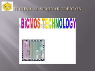

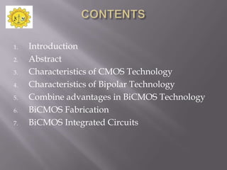
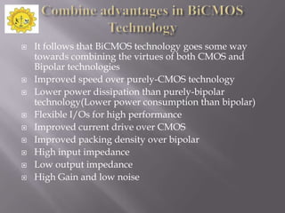
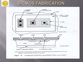
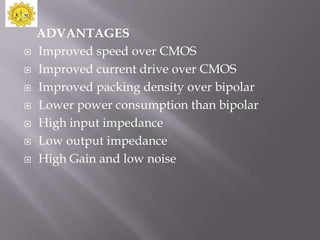


The document discusses a technical seminar on BiCMOS technology. It begins with an introduction and describes the characteristics and fabrication processes of CMOS, bipolar, and BiCMOS technologies. BiCMOS combines the advantages of CMOS, like low power and high density, with bipolar's high speed and current drive. While more complex than CMOS, BiCMOS provides improved performance over both CMOS and bipolar. The document outlines the advantages and applications of BiCMOS, such as mixed-signal integrated circuits, and compares it to CMOS and bipolar technologies. It concludes with a literature survey on books and websites relating to BiCMOS design.