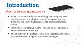
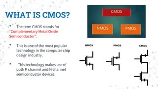
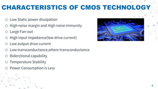
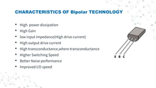
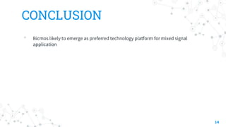
TECHNICAL SEMINAR
BiCMOS TECHNOLOGY
KEERTHI PATIL
19261A04E6
ECE-3
CONTENTS
2
 INTRODUCTION
 HISTORY
 CMOS Technology and its Characteristics
 Bipolar Technology and its Characteristics
 BiCMOS Fabrication
 BiCMOS Integrated circuits
 Advantages and Disadvantages of BiCMOS Technology
 Applications of BiCMOS
 Comparison between CMOS and BiCMOS
 BiCMOS Products
 CONCLUSION
Introduction
ļ‚§ BiCMOS is a semiconductor Technology that integrates two
semiconductor technologies, those of the bipolar junction
transistor and the CMOS logic gate, into a single integrated
circuit.
ļ‚§ In BiCMOS Technology, both the MOS and bipolar devices are
fabricated on the Same Chip.
ļ‚§ The objective of the BiCMOS is to combine bipolar and CMOS as
to exploit the advantages of both the technologies.
3
What is BiCMOS Technology ?
HISTORY
• The history of semiconductor devices started in 1930’s when
LIENFED and HEIL first proposed the MOSFET.
• Bipolar Technology was started in 1980’s.
• CMOS Technology was also started in mid 1980’s.
• Later in 1990 there was a cross over between bipolar and CMOS
Technology.
• Now we are in 3rd Generation BICMOS Technology.
4
WHAT IS CMOS?
• The term CMOS stands for
ā€œComplementary Metal Oxide
Semiconductorā€.
• This is one of the most popular
technology in the computer chip
design industry.
• This technology makes use of
both P channel and N channel
semiconductor devices.
CHARACTERISTICS OF CMOS TECHNOLOGY
o Low Static power dissipation
o High noise margin and High noise immunity
o Large Fan-out
o High input impedance(low drive current)
o Low output drive current
o Low transconductance,where transconductance
o Biderctional capability
o Temperature Stability
o Power Consumption is Less
6
WHAT IS BJT?
ļ‚§ A bipolar junction transistor is a three-
terminal semiconductor device that
consists of two p-n junctions which
are able to amplify or magnify a
signal.
ļ‚§ It is a current controlled device.
ļ‚§ The three terminals of the BJT are the
base, the collector, and the emitter.
CHARACTERISTICS OF Bipolar TECHNOLOGY
• High power dissipation
• High Gain
• low input impedance(High drive current)
• High output drive current
• High transconductance,where transconductance
• Higher Switching Speed
• Better Noise performance
• Improved I/O speed
BiCMOS Integrated Circuits
9
ADVANTAGES
• Improved speed over CMOS
• Improved current drive over CMOS
• Improved packing density over bipolar
• Lower power dissipation than bipolar
• High input impedance
• Low output impedance
• High Gain and low noise
• Flexible I/O’s for high performance
10
DISADVANTAGES
• Process Complexity
• High cost
• Longer Fabrication cycle time
• Speed degradation due to scaling
11
APPLICATIONS
• Full custom ICS
• ALU’S, Barrel Shifters
• SRAM,DRAM
• Microprocessor, MicroController
• Semi custom ICs
• Register , Flipflop, Standard cells
• Adders , mixers , ADC , DAC
• Gate arrays
• Flash A/D Converters
12
COMPARISION BETWEEN CMOS & BiCMOS
13
CONCLUSION
• Bicmos likely to emerge as preferred technology platform for mixed signal
application
14

4e6 ppt bicmos NEW.pptx

  • 1.
  • 2.
    CONTENTS 2  INTRODUCTION  HISTORY CMOS Technology and its Characteristics  Bipolar Technology and its Characteristics  BiCMOS Fabrication  BiCMOS Integrated circuits  Advantages and Disadvantages of BiCMOS Technology  Applications of BiCMOS  Comparison between CMOS and BiCMOS  BiCMOS Products  CONCLUSION
  • 3.
    Introduction ļ‚§ BiCMOS isa semiconductor Technology that integrates two semiconductor technologies, those of the bipolar junction transistor and the CMOS logic gate, into a single integrated circuit. ļ‚§ In BiCMOS Technology, both the MOS and bipolar devices are fabricated on the Same Chip. ļ‚§ The objective of the BiCMOS is to combine bipolar and CMOS as to exploit the advantages of both the technologies. 3 What is BiCMOS Technology ?
  • 4.
    HISTORY • The historyof semiconductor devices started in 1930’s when LIENFED and HEIL first proposed the MOSFET. • Bipolar Technology was started in 1980’s. • CMOS Technology was also started in mid 1980’s. • Later in 1990 there was a cross over between bipolar and CMOS Technology. • Now we are in 3rd Generation BICMOS Technology. 4
  • 5.
    WHAT IS CMOS? •The term CMOS stands for ā€œComplementary Metal Oxide Semiconductorā€. • This is one of the most popular technology in the computer chip design industry. • This technology makes use of both P channel and N channel semiconductor devices.
  • 6.
    CHARACTERISTICS OF CMOSTECHNOLOGY o Low Static power dissipation o High noise margin and High noise immunity o Large Fan-out o High input impedance(low drive current) o Low output drive current o Low transconductance,where transconductance o Biderctional capability o Temperature Stability o Power Consumption is Less 6
  • 7.
    WHAT IS BJT? ļ‚§A bipolar junction transistor is a three- terminal semiconductor device that consists of two p-n junctions which are able to amplify or magnify a signal. ļ‚§ It is a current controlled device. ļ‚§ The three terminals of the BJT are the base, the collector, and the emitter.
  • 8.
    CHARACTERISTICS OF BipolarTECHNOLOGY • High power dissipation • High Gain • low input impedance(High drive current) • High output drive current • High transconductance,where transconductance • Higher Switching Speed • Better Noise performance • Improved I/O speed
  • 9.
  • 10.
    ADVANTAGES • Improved speedover CMOS • Improved current drive over CMOS • Improved packing density over bipolar • Lower power dissipation than bipolar • High input impedance • Low output impedance • High Gain and low noise • Flexible I/O’s for high performance 10
  • 11.
    DISADVANTAGES • Process Complexity •High cost • Longer Fabrication cycle time • Speed degradation due to scaling 11
  • 12.
    APPLICATIONS • Full customICS • ALU’S, Barrel Shifters • SRAM,DRAM • Microprocessor, MicroController • Semi custom ICs • Register , Flipflop, Standard cells • Adders , mixers , ADC , DAC • Gate arrays • Flash A/D Converters 12
  • 13.
  • 14.
    CONCLUSION • Bicmos likelyto emerge as preferred technology platform for mixed signal application 14