8. Advantages ofBiCMOS
9. Disadvantages of BiCMOS
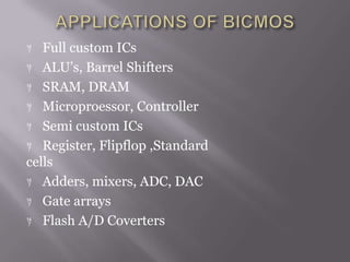
10.Applications of BiCMOS
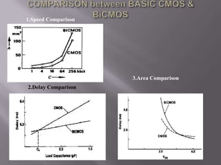
11.Comparison between CMOS and BiCMOS
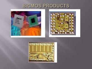
12.BiCMOS Products
13.Conclusion
4.
The historyof semiconductor devices started in
1930’s when Lienfed and Heil first proposed
the mosfet.
Bipolar Technology was started in 1980’s.
CMOS Technology was also started in mid
1980’s.
Later in 1990 there was a cross over between
bipolar and CMOS Technology.
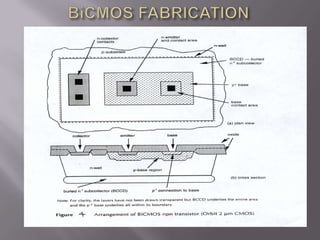
In BiCMOS technology, both the MOS and
bipolar device are fabricated on the same chip .
5.
The objectiveof the BiCMOS is to combine
bipolar and CMOS so as to exploit the
advantages of both the technlogies.
Today BiCMOS has become one of the
dominant technologies used for high
speed, low power and highly functional VLSI
circuits.
The process step required for both CMOS and
bipolar are similar so the BiCMOS process has
been enhanced and integrated into the CMOS
process without any additional steps.
6.
The primaryapproach to realize high performance
BiCMOS devices is the addition of bipolar process
steps to a baseline CMOS process.
The BiCMOS gates could be used as an effective
way of speeding up the VLSI circuits.
The applications of BiCMOS are vast.
Advantages of bipolar and CMOS circuits can be
retained in BiCMOS chips.
BiCMOS technology enables high performance
integrated circuits IC’s but increases process
complexity.
7.
BiCMOS technologyis a combination of
Bipolar and CMOS technology.
CMOS technology offers less power
dissipation, smaller noise margins, and higher
packing density.
Bipolar technology, on the other hand, ensures
high switching and I/O speed and good noise
performance
Now we are in 3rd Generation BiCMOS
Technology.
8.
BiCMOS technologyaccomplishes both -
improved speed over CMOS and lower power
dissipation than bipolar technology.
The main drawback of BiCMOS technology is
the higher costs due to the added process
complexity.
This greater process complexity in BiCMOS
results in a cost increase compared to
conventional CMOS technology.
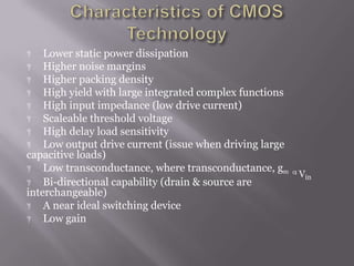
9.
Vin
Lower staticpower dissipation
Higher noise margins
Higher packing density
High yield with large integrated complex functions
High input impedance (low drive current)
Scaleable threshold voltage
High delay load sensitivity
Low output drive current (issue when driving large
capacitive loads)
Low transconductance, where transconductance, gm
Bi-directional capability (drain & source are
interchangeable)
A near ideal switching device
Low gain
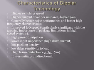
10.
Higher switchingspeed
Higher current drive per unit area, higher gain
Generally better noise performance and better high
frequency characteristics
Improved I/O speed (particularly significant with the
growing importance of package limitations in high
speed systems).
high power dissipation
lower input impedance (high drive current)
low packing density
low delay sensitivity to load
High transconductance gm (gm Vin)
It is essentially unidirectional.
11.
It followsthat BiCMOS technology goes some way
towards combining the virtues of both CMOS and
Bipolar technologies
Improved speed over purely-CMOS technology
Lower power dissipation than purely-bipolar
technology(Lower power consumption than bipolar)
Flexible I/Os for high performance
Improved current drive over CMOS
Improved packing density over bipolar
High input impedance
Low output impedance
High Gain and low noise
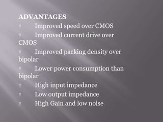
ADVANTAGES
Improved speedover CMOS
Improved current drive over
CMOS
Improved packing density over
bipolar
Lower power consumption than
bipolar
High input impedance
Low output impedance
High Gain and low noise
15.
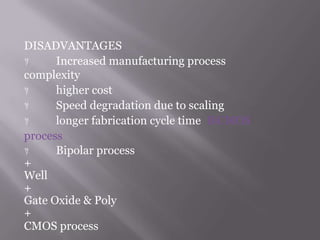
DISADVANTAGES
Increased manufacturingprocess
complexity
higher cost
Speed degradation due to scaling
longer fabrication cycle time BiCMOS
process
Bipolar process
+
Well
+
Gate Oxide & Poly
+
CMOS process
LITERATURE SURVEY
BOOKS:
VLSI BasicDesign by Douglas A. Pucknell and
Kamran Eshraghian
WEBSITES: http://www.vlsihandbook.com
http://www.bicmosdesign.com
http://website.informer.com
http://www.freepatentsonline.com/6927460.html