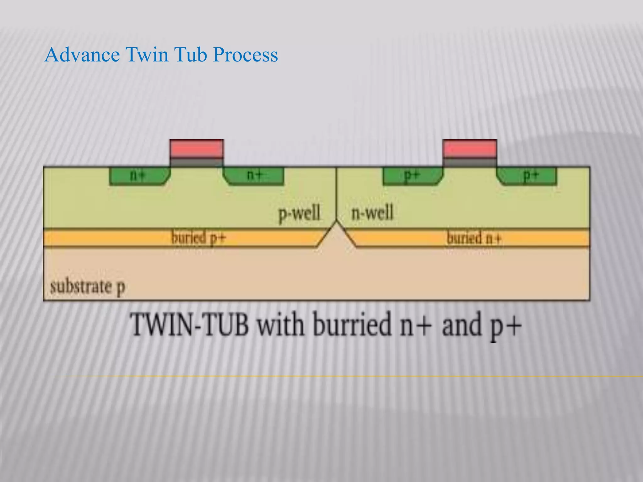
SlideShare a Scribd company logo
Applied Electronics –PT
Coimbatore - india
Twin well Process
Provide separate optimization of the n-type and p-type transistors
This means that transistor parameters such as threshold voltage, body
effect and the channel transconductance of both types of transistors can be
tuned independently
n+ or p+ substrate, with a lightly doped epitaxial layer on top, forms the
starting material for this technology.
The n-well and pwell are formed on this epitaxial layer which forms the
actual substrate.
The dopant concentrations can be carefully optimized to produce the
desired device characteristics because two independent doping steps are
performed to create the well regions.
The starting material is either an n+ or p+ substrate with a lightly doped
epitaxial layer, which is used for protection against latch up
This process provides separately optimized wells, balanced performance n-
transistors and p-transistors may be constructed
Tub formation
 Thin-oxide construction
 Source and drain implantations
 Contact cut definition
 Metallization
Twin well Process Continued…,
Twin well Process Steps
Step1:
N or p type substrate is taken Initially
Step2:
Epitaxial Layer Deposition, Lightly Doped Epitaxial Layer is
Deposited above n+ or p+ Substrate.
Electrical Properties of Layer is Fixed by Dopant and its
Concentration.
The Aim of This Step is to Deposite High-Purity Silicon Layer.
Concentration of Dopant Distributed Throught the Layer
Step3:
Tub Formation
n -well-Formation
Protect certain region in this by using an oxide nitride mask
Phosphorus implantation
Form n-well
Entire substrate to an oxidation process
The oxide is going to be formed only over the n-well
The rest of the portions are protected by the oxide nitride mask
This n-well will also be driven deeper
Step4:
p -well-Formation
Protect certain region in this by using an oxide nitride mask
Boron implantation
Form p-well
Entire substrate to an oxidation process
Implant The p-well
Step 5:
Polysilicon Layer is Formed The Overall Surface
Step 6:
Polysilicon gates Are Formed for n-well and p-well by Using Photo-Etching
Process
Step 7:
Using Blanket Implantation(Auto Aligning The Wells)
Step 8:
n+ Diffusion is Formed in n-well
p+ Diffusion is Formed in p-well
These Are Used For VDD and VSS Contacts(Substrate Formation)
Step9:
Contact Cuts Are Defined In Both The Wells
Step10:
Metalization Process (Metal Contacts Are Created)
p-
p-epitaxial
p well N well
p+n+
gate oxide
Al (Cu)
tungsten
SiO2
SiO2
TiSi2
Dual-Well Trench-Isolated CMOS
field oxide
Advantages of Twin Tub Method:
Separate Optimized Wells Are Available
Balanced Performance of N and P Transistors is Obtained(Speciality)
Advance Twin Tub Process
Twin well process

More Related Content

What's hot

N well
N wellN well
CMOS fabrication n well process
CMOS fabrication n well processCMOS fabrication n well process
CMOS fabrication n well process
SouvikDatta22
 
Device isolation Techniques
Device isolation TechniquesDevice isolation Techniques
Device isolation Techniques
Sudhanshu Janwadkar
 
Second order effects
Second order effectsSecond order effects
Second order effects
PRAVEEN KUMAR CHITLURI
 
Silicon on Insulator (SOI) Technology
Silicon on Insulator (SOI) TechnologySilicon on Insulator (SOI) Technology
Silicon on Insulator (SOI) Technology
Sudhanshu Janwadkar
 
MOS transistor 13
MOS transistor 13MOS transistor 13
MOS transistor 13
HIMANSHU DIWAKAR
 
MOSFET and Short channel effects
MOSFET and Short channel effectsMOSFET and Short channel effects
MOSFET and Short channel effects
Lee Rather
 
SHORT CHANNEL EFFECTS IN MOSFETS- VLSI DESIGN
SHORT CHANNEL EFFECTS IN MOSFETS- VLSI DESIGNSHORT CHANNEL EFFECTS IN MOSFETS- VLSI DESIGN
SHORT CHANNEL EFFECTS IN MOSFETS- VLSI DESIGN
NITHIN KALLE PALLY
 
Channel length Modulation
Channel length ModulationChannel length Modulation
Channel length Modulation
Engineering Funda
 
MOS Capacitor
MOS CapacitorMOS Capacitor
VLSI Design(Fabrication)
VLSI Design(Fabrication)VLSI Design(Fabrication)
VLSI Design(Fabrication)
Trijit Mallick
 
CMOS
CMOS CMOS
Short channel effects
Short channel effectsShort channel effects
Short channel effects
aditiagrawal97
 
Pass Transistor Logic
Pass Transistor LogicPass Transistor Logic
Pass Transistor LogicDiwaker Pant
 
MOS as Diode, Switch and Active Resistor
MOS as Diode, Switch and Active ResistorMOS as Diode, Switch and Active Resistor
MOS as Diode, Switch and Active Resistor
Sudhanshu Janwadkar
 
Fabrication steps of IC
Fabrication steps of ICFabrication steps of IC
Fabrication steps of IC
Gowri Kishore
 
Finfets
FinfetsFinfets
Cmos design
Cmos designCmos design
Cmos designMahi
 
Rc delay modelling in vlsi
Rc delay modelling in vlsiRc delay modelling in vlsi
Rc delay modelling in vlsi
Dr. Vishal Sharma
 

What's hot (20)

N well
N wellN well
N well
 
CMOS fabrication n well process
CMOS fabrication n well processCMOS fabrication n well process
CMOS fabrication n well process
 
Device isolation Techniques
Device isolation TechniquesDevice isolation Techniques
Device isolation Techniques
 
Second order effects
Second order effectsSecond order effects
Second order effects
 
Silicon on Insulator (SOI) Technology
Silicon on Insulator (SOI) TechnologySilicon on Insulator (SOI) Technology
Silicon on Insulator (SOI) Technology
 
MOS transistor 13
MOS transistor 13MOS transistor 13
MOS transistor 13
 
MOSFET and Short channel effects
MOSFET and Short channel effectsMOSFET and Short channel effects
MOSFET and Short channel effects
 
15 mosfet threshold voltage
15 mosfet threshold voltage15 mosfet threshold voltage
15 mosfet threshold voltage
 
SHORT CHANNEL EFFECTS IN MOSFETS- VLSI DESIGN
SHORT CHANNEL EFFECTS IN MOSFETS- VLSI DESIGNSHORT CHANNEL EFFECTS IN MOSFETS- VLSI DESIGN
SHORT CHANNEL EFFECTS IN MOSFETS- VLSI DESIGN
 
Channel length Modulation
Channel length ModulationChannel length Modulation
Channel length Modulation
 
MOS Capacitor
MOS CapacitorMOS Capacitor
MOS Capacitor
 
VLSI Design(Fabrication)
VLSI Design(Fabrication)VLSI Design(Fabrication)
VLSI Design(Fabrication)
 
CMOS
CMOS CMOS
CMOS
 
Short channel effects
Short channel effectsShort channel effects
Short channel effects
 
Pass Transistor Logic
Pass Transistor LogicPass Transistor Logic
Pass Transistor Logic
 
MOS as Diode, Switch and Active Resistor
MOS as Diode, Switch and Active ResistorMOS as Diode, Switch and Active Resistor
MOS as Diode, Switch and Active Resistor
 
Fabrication steps of IC
Fabrication steps of ICFabrication steps of IC
Fabrication steps of IC
 
Finfets
FinfetsFinfets
Finfets
 
Cmos design
Cmos designCmos design
Cmos design
 
Rc delay modelling in vlsi
Rc delay modelling in vlsiRc delay modelling in vlsi
Rc delay modelling in vlsi
 

Similar to Twin well process

Lecture4 nmos process
Lecture4 nmos processLecture4 nmos process
Lecture4 nmos process
sritulasiadigopula
 
TWIN TAB PROCESSING
TWIN TAB PROCESSINGTWIN TAB PROCESSING
TWIN TAB PROCESSING
nandininadesan
 
3. CMOS Fabrication.ppt important to read
3. CMOS Fabrication.ppt important to read3. CMOS Fabrication.ppt important to read
3. CMOS Fabrication.ppt important to read
Sahithikairamkonda
 
Chapter2 VLSI.pptx
Chapter2 VLSI.pptxChapter2 VLSI.pptx
Chapter2 VLSI.pptx
AshishSoni509
 
CMOS N-WELL.pptx
CMOS N-WELL.pptxCMOS N-WELL.pptx
CMOS N-WELL.pptx
Balaji391305
 
Cmos fabrication
Cmos fabricationCmos fabrication
Cmos fabrication
KANAGARAJ T
 
VLSI-mosfet-construction engineering ECE
VLSI-mosfet-construction engineering ECEVLSI-mosfet-construction engineering ECE
VLSI-mosfet-construction engineering ECE
jpradha86
 
Module-1.pptx
Module-1.pptxModule-1.pptx
Module-1.pptx
8885684828
 
Vlsi design notes(1st unit) according to vtu syllabus.(BE)
Vlsi  design notes(1st unit) according to vtu syllabus.(BE)Vlsi  design notes(1st unit) according to vtu syllabus.(BE)
Vlsi design notes(1st unit) according to vtu syllabus.(BE)
instrumentation_vtu
 
IC fabrication and its types with real life applications.pptx
IC fabrication and its types with real life applications.pptxIC fabrication and its types with real life applications.pptx
IC fabrication and its types with real life applications.pptx
Nishanth Asmi
 
99997340.pdf
99997340.pdf99997340.pdf
99997340.pdf
RaunakKumar33449
 
CMOS N P Twin Tub Well Formation
CMOS N P Twin Tub Well FormationCMOS N P Twin Tub Well Formation
CMOS N P Twin Tub Well Formation
azmathmoosa
 
My VLSI.pptx
My VLSI.pptxMy VLSI.pptx
My VLSI.pptx
chiranjeevimuppala2
 
N well process
N well processN well process
N well process
NeetiYadav7
 
Monolithic implementation of parasitic elements
Monolithic implementation of parasitic elementsMonolithic implementation of parasitic elements
Monolithic implementation of parasitic elements
GOPICHAND NAGUBOINA
 
Lect2 up030 (100324)
Lect2 up030 (100324)Lect2 up030 (100324)
Lect2 up030 (100324)aicdesign
 
WORK FUNCTION ESTIMATION OF BISMUTH DOPED ZNO THIN FILM
WORK FUNCTION ESTIMATION OF BISMUTH DOPED ZNO THIN FILMWORK FUNCTION ESTIMATION OF BISMUTH DOPED ZNO THIN FILM
WORK FUNCTION ESTIMATION OF BISMUTH DOPED ZNO THIN FILM
antjjournal
 
Sp15 bee-112(fabrication)
Sp15 bee-112(fabrication)Sp15 bee-112(fabrication)
Sp15 bee-112(fabrication)
Anjum Aftab Mirza
 

Similar to Twin well process (20)

Vlsi 2
Vlsi 2Vlsi 2
Vlsi 2
 
Lecture4 nmos process
Lecture4 nmos processLecture4 nmos process
Lecture4 nmos process
 
TWIN TAB PROCESSING
TWIN TAB PROCESSINGTWIN TAB PROCESSING
TWIN TAB PROCESSING
 
3. CMOS Fabrication.ppt important to read
3. CMOS Fabrication.ppt important to read3. CMOS Fabrication.ppt important to read
3. CMOS Fabrication.ppt important to read
 
Chapter2 VLSI.pptx
Chapter2 VLSI.pptxChapter2 VLSI.pptx
Chapter2 VLSI.pptx
 
CMOS N-WELL.pptx
CMOS N-WELL.pptxCMOS N-WELL.pptx
CMOS N-WELL.pptx
 
Cmos fabrication
Cmos fabricationCmos fabrication
Cmos fabrication
 
VLSI-mosfet-construction engineering ECE
VLSI-mosfet-construction engineering ECEVLSI-mosfet-construction engineering ECE
VLSI-mosfet-construction engineering ECE
 
Module-1.pptx
Module-1.pptxModule-1.pptx
Module-1.pptx
 
Vlsi design notes(1st unit) according to vtu syllabus.(BE)
Vlsi  design notes(1st unit) according to vtu syllabus.(BE)Vlsi  design notes(1st unit) according to vtu syllabus.(BE)
Vlsi design notes(1st unit) according to vtu syllabus.(BE)
 
IC fabrication and its types with real life applications.pptx
IC fabrication and its types with real life applications.pptxIC fabrication and its types with real life applications.pptx
IC fabrication and its types with real life applications.pptx
 
99997340.pdf
99997340.pdf99997340.pdf
99997340.pdf
 
CMOS N P Twin Tub Well Formation
CMOS N P Twin Tub Well FormationCMOS N P Twin Tub Well Formation
CMOS N P Twin Tub Well Formation
 
My VLSI.pptx
My VLSI.pptxMy VLSI.pptx
My VLSI.pptx
 
N well process
N well processN well process
N well process
 
Monolithic implementation of parasitic elements
Monolithic implementation of parasitic elementsMonolithic implementation of parasitic elements
Monolithic implementation of parasitic elements
 
Lect2 up030 (100324)
Lect2 up030 (100324)Lect2 up030 (100324)
Lect2 up030 (100324)
 
WORK FUNCTION ESTIMATION OF BISMUTH DOPED ZNO THIN FILM
WORK FUNCTION ESTIMATION OF BISMUTH DOPED ZNO THIN FILMWORK FUNCTION ESTIMATION OF BISMUTH DOPED ZNO THIN FILM
WORK FUNCTION ESTIMATION OF BISMUTH DOPED ZNO THIN FILM
 
Sp15 bee-112(fabrication)
Sp15 bee-112(fabrication)Sp15 bee-112(fabrication)
Sp15 bee-112(fabrication)
 
Vlsi 1
Vlsi 1Vlsi 1
Vlsi 1
 

Recently uploaded

DESIGN A COTTON SEED SEPARATION MACHINE.docx
DESIGN A COTTON SEED SEPARATION MACHINE.docxDESIGN A COTTON SEED SEPARATION MACHINE.docx
DESIGN A COTTON SEED SEPARATION MACHINE.docx
FluxPrime1
 
ethical hacking in wireless-hacking1.ppt
ethical hacking in wireless-hacking1.pptethical hacking in wireless-hacking1.ppt
ethical hacking in wireless-hacking1.ppt
Jayaprasanna4
 
Democratizing Fuzzing at Scale by Abhishek Arya
Democratizing Fuzzing at Scale by Abhishek AryaDemocratizing Fuzzing at Scale by Abhishek Arya
Democratizing Fuzzing at Scale by Abhishek Arya
abh.arya
 
Automobile Management System Project Report.pdf
Automobile Management System Project Report.pdfAutomobile Management System Project Report.pdf
Automobile Management System Project Report.pdf
Kamal Acharya
 
Forklift Classes Overview by Intella Parts
Forklift Classes Overview by Intella PartsForklift Classes Overview by Intella Parts
Forklift Classes Overview by Intella Parts
Intella Parts
 
Hybrid optimization of pumped hydro system and solar- Engr. Abdul-Azeez.pdf
Hybrid optimization of pumped hydro system and solar- Engr. Abdul-Azeez.pdfHybrid optimization of pumped hydro system and solar- Engr. Abdul-Azeez.pdf
Hybrid optimization of pumped hydro system and solar- Engr. Abdul-Azeez.pdf
fxintegritypublishin
 
WATER CRISIS and its solutions-pptx 1234
WATER CRISIS and its solutions-pptx 1234WATER CRISIS and its solutions-pptx 1234
WATER CRISIS and its solutions-pptx 1234
AafreenAbuthahir2
 
Final project report on grocery store management system..pdf
Final project report on grocery store management system..pdfFinal project report on grocery store management system..pdf
Final project report on grocery store management system..pdf
Kamal Acharya
 
Sachpazis:Terzaghi Bearing Capacity Estimation in simple terms with Calculati...
Sachpazis:Terzaghi Bearing Capacity Estimation in simple terms with Calculati...Sachpazis:Terzaghi Bearing Capacity Estimation in simple terms with Calculati...
Sachpazis:Terzaghi Bearing Capacity Estimation in simple terms with Calculati...
Dr.Costas Sachpazis
 
Student information management system project report ii.pdf
Student information management system project report ii.pdfStudent information management system project report ii.pdf
Student information management system project report ii.pdf
Kamal Acharya
 
NO1 Uk best vashikaran specialist in delhi vashikaran baba near me online vas...
NO1 Uk best vashikaran specialist in delhi vashikaran baba near me online vas...NO1 Uk best vashikaran specialist in delhi vashikaran baba near me online vas...
NO1 Uk best vashikaran specialist in delhi vashikaran baba near me online vas...
Amil Baba Dawood bangali
 
Standard Reomte Control Interface - Neometrix
Standard Reomte Control Interface - NeometrixStandard Reomte Control Interface - Neometrix
Standard Reomte Control Interface - Neometrix
Neometrix_Engineering_Pvt_Ltd
 
Water Industry Process Automation and Control Monthly - May 2024.pdf
Water Industry Process Automation and Control Monthly - May 2024.pdfWater Industry Process Automation and Control Monthly - May 2024.pdf
Water Industry Process Automation and Control Monthly - May 2024.pdf
Water Industry Process Automation & Control
 
Halogenation process of chemical process industries
Halogenation process of chemical process industriesHalogenation process of chemical process industries
Halogenation process of chemical process industries
MuhammadTufail242431
 
addressing modes in computer architecture
addressing modes  in computer architectureaddressing modes  in computer architecture
addressing modes in computer architecture
ShahidSultan24
 
power quality voltage fluctuation UNIT - I.pptx
power quality voltage fluctuation UNIT - I.pptxpower quality voltage fluctuation UNIT - I.pptx
power quality voltage fluctuation UNIT - I.pptx
ViniHema
 
Railway Signalling Principles Edition 3.pdf
Railway Signalling Principles Edition 3.pdfRailway Signalling Principles Edition 3.pdf
Railway Signalling Principles Edition 3.pdf
TeeVichai
 
CME397 Surface Engineering- Professional Elective
CME397 Surface Engineering- Professional ElectiveCME397 Surface Engineering- Professional Elective
CME397 Surface Engineering- Professional Elective
karthi keyan
 
Quality defects in TMT Bars, Possible causes and Potential Solutions.
Quality defects in TMT Bars, Possible causes and Potential Solutions.Quality defects in TMT Bars, Possible causes and Potential Solutions.
Quality defects in TMT Bars, Possible causes and Potential Solutions.
PrashantGoswami42
 
block diagram and signal flow graph representation
block diagram and signal flow graph representationblock diagram and signal flow graph representation
block diagram and signal flow graph representation
Divya Somashekar
 

Recently uploaded (20)

DESIGN A COTTON SEED SEPARATION MACHINE.docx
DESIGN A COTTON SEED SEPARATION MACHINE.docxDESIGN A COTTON SEED SEPARATION MACHINE.docx
DESIGN A COTTON SEED SEPARATION MACHINE.docx
 
ethical hacking in wireless-hacking1.ppt
ethical hacking in wireless-hacking1.pptethical hacking in wireless-hacking1.ppt
ethical hacking in wireless-hacking1.ppt
 
Democratizing Fuzzing at Scale by Abhishek Arya
Democratizing Fuzzing at Scale by Abhishek AryaDemocratizing Fuzzing at Scale by Abhishek Arya
Democratizing Fuzzing at Scale by Abhishek Arya
 
Automobile Management System Project Report.pdf
Automobile Management System Project Report.pdfAutomobile Management System Project Report.pdf
Automobile Management System Project Report.pdf
 
Forklift Classes Overview by Intella Parts
Forklift Classes Overview by Intella PartsForklift Classes Overview by Intella Parts
Forklift Classes Overview by Intella Parts
 
Hybrid optimization of pumped hydro system and solar- Engr. Abdul-Azeez.pdf
Hybrid optimization of pumped hydro system and solar- Engr. Abdul-Azeez.pdfHybrid optimization of pumped hydro system and solar- Engr. Abdul-Azeez.pdf
Hybrid optimization of pumped hydro system and solar- Engr. Abdul-Azeez.pdf
 
WATER CRISIS and its solutions-pptx 1234
WATER CRISIS and its solutions-pptx 1234WATER CRISIS and its solutions-pptx 1234
WATER CRISIS and its solutions-pptx 1234
 
Final project report on grocery store management system..pdf
Final project report on grocery store management system..pdfFinal project report on grocery store management system..pdf
Final project report on grocery store management system..pdf
 
Sachpazis:Terzaghi Bearing Capacity Estimation in simple terms with Calculati...
Sachpazis:Terzaghi Bearing Capacity Estimation in simple terms with Calculati...Sachpazis:Terzaghi Bearing Capacity Estimation in simple terms with Calculati...
Sachpazis:Terzaghi Bearing Capacity Estimation in simple terms with Calculati...
 
Student information management system project report ii.pdf
Student information management system project report ii.pdfStudent information management system project report ii.pdf
Student information management system project report ii.pdf
 
NO1 Uk best vashikaran specialist in delhi vashikaran baba near me online vas...
NO1 Uk best vashikaran specialist in delhi vashikaran baba near me online vas...NO1 Uk best vashikaran specialist in delhi vashikaran baba near me online vas...
NO1 Uk best vashikaran specialist in delhi vashikaran baba near me online vas...
 
Standard Reomte Control Interface - Neometrix
Standard Reomte Control Interface - NeometrixStandard Reomte Control Interface - Neometrix
Standard Reomte Control Interface - Neometrix
 
Water Industry Process Automation and Control Monthly - May 2024.pdf
Water Industry Process Automation and Control Monthly - May 2024.pdfWater Industry Process Automation and Control Monthly - May 2024.pdf
Water Industry Process Automation and Control Monthly - May 2024.pdf
 
Halogenation process of chemical process industries
Halogenation process of chemical process industriesHalogenation process of chemical process industries
Halogenation process of chemical process industries
 
addressing modes in computer architecture
addressing modes  in computer architectureaddressing modes  in computer architecture
addressing modes in computer architecture
 
power quality voltage fluctuation UNIT - I.pptx
power quality voltage fluctuation UNIT - I.pptxpower quality voltage fluctuation UNIT - I.pptx
power quality voltage fluctuation UNIT - I.pptx
 
Railway Signalling Principles Edition 3.pdf
Railway Signalling Principles Edition 3.pdfRailway Signalling Principles Edition 3.pdf
Railway Signalling Principles Edition 3.pdf
 
CME397 Surface Engineering- Professional Elective
CME397 Surface Engineering- Professional ElectiveCME397 Surface Engineering- Professional Elective
CME397 Surface Engineering- Professional Elective
 
Quality defects in TMT Bars, Possible causes and Potential Solutions.
Quality defects in TMT Bars, Possible causes and Potential Solutions.Quality defects in TMT Bars, Possible causes and Potential Solutions.
Quality defects in TMT Bars, Possible causes and Potential Solutions.
 
block diagram and signal flow graph representation
block diagram and signal flow graph representationblock diagram and signal flow graph representation
block diagram and signal flow graph representation
 

Twin well process

  • 2. Twin well Process Provide separate optimization of the n-type and p-type transistors This means that transistor parameters such as threshold voltage, body effect and the channel transconductance of both types of transistors can be tuned independently n+ or p+ substrate, with a lightly doped epitaxial layer on top, forms the starting material for this technology. The n-well and pwell are formed on this epitaxial layer which forms the actual substrate. The dopant concentrations can be carefully optimized to produce the desired device characteristics because two independent doping steps are performed to create the well regions.
  • 3. The starting material is either an n+ or p+ substrate with a lightly doped epitaxial layer, which is used for protection against latch up This process provides separately optimized wells, balanced performance n- transistors and p-transistors may be constructed Tub formation  Thin-oxide construction  Source and drain implantations  Contact cut definition  Metallization Twin well Process Continued…,
  • 4. Twin well Process Steps Step1: N or p type substrate is taken Initially Step2: Epitaxial Layer Deposition, Lightly Doped Epitaxial Layer is Deposited above n+ or p+ Substrate. Electrical Properties of Layer is Fixed by Dopant and its Concentration. The Aim of This Step is to Deposite High-Purity Silicon Layer. Concentration of Dopant Distributed Throught the Layer Step3: Tub Formation n -well-Formation Protect certain region in this by using an oxide nitride mask Phosphorus implantation Form n-well Entire substrate to an oxidation process The oxide is going to be formed only over the n-well The rest of the portions are protected by the oxide nitride mask This n-well will also be driven deeper
  • 5. Step4: p -well-Formation Protect certain region in this by using an oxide nitride mask Boron implantation Form p-well Entire substrate to an oxidation process Implant The p-well Step 5: Polysilicon Layer is Formed The Overall Surface Step 6: Polysilicon gates Are Formed for n-well and p-well by Using Photo-Etching Process Step 7: Using Blanket Implantation(Auto Aligning The Wells) Step 8: n+ Diffusion is Formed in n-well p+ Diffusion is Formed in p-well These Are Used For VDD and VSS Contacts(Substrate Formation)
  • 6. Step9: Contact Cuts Are Defined In Both The Wells Step10: Metalization Process (Metal Contacts Are Created)
  • 7. p- p-epitaxial p well N well p+n+ gate oxide Al (Cu) tungsten SiO2 SiO2 TiSi2 Dual-Well Trench-Isolated CMOS field oxide
  • 8. Advantages of Twin Tub Method: Separate Optimized Wells Are Available Balanced Performance of N and P Transistors is Obtained(Speciality)