BiCMOS technology incorporates both bipolar junction transistors and CMOS transistors on a single integrated circuit. This allows for circuits with higher speed, power, and density than either bipolar or CMOS alone. BiCMOS provides the high speed of bipolar transistors along with the low power advantages of CMOS transistors. It is used in applications such as microprocessors, memories, analog circuits, and mixed-signal circuits that require both analog and digital components.
What is BiCMOS?
This is one of the major semiconductor technologies and is a highly developed
technology
In 1990s, two separate technologies were incorporated, namely bipolar junction
transistor (offering high speed and gain) and CMOS transistor (excels for constructing
simple, low-power logic gates) in a single modern integrated circuit.
BiCMOS is able to achieve VLSI circuits with speed-power-density performance
previously unattainable with either technology individually.
3.
VLSI Circuits
⢠Very-large-scaleintegration (VLSI) is the process of creating
an integrated circuit (IC) by combining billions of transistors into a single
chip.
⢠VLSI began in the 1970s when complex semiconductor and communication
technologies were being developed.
⢠VLSI helped in integrating a CPU, ROM, RAM and other glue logic into
one chip. The microprocessor is a VLSI device.
4.
A VLSI ICDIE
Courtesy: Wikipedia ( GNU Free
Documentation License)
5.
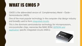
WHAT IS CMOS?
CMOS is the abbreviated version of Complementary Metal ā Oxide ā
Semiconductor (MOS).
One of the most popular technology in the computer chip design industry
and broadly used to form integrated circuits.
This is the dominant semiconductor technology for microprocessors,
microcontroller chips, memories like RAM, ROM, EEPROM and
application specific integrated circuits (ASICs).
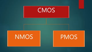
NMOS
ļµ NMOS isbuilt on a p-type substrate with n-type source and drain
diffused on it.
ļµ In NMOS, the majority carriers are electrons. Therefore, much faster than
PMOS.
ļµ NMOS will conduct when high voltage is applied to the gate.
8.
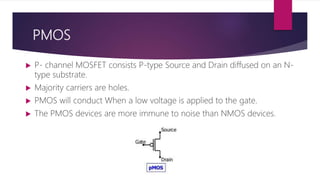
PMOS
ļµ P- channelMOSFET consists P-type Source and Drain diffused on an N-
type substrate.
ļµ Majority carriers are holes.
ļµ PMOS will conduct When a low voltage is applied to the gate.
ļµ The PMOS devices are more immune to noise than NMOS devices.
9.
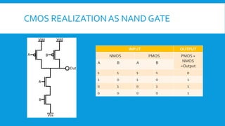
CMOS REALIZATION ASNAND GATE
INPUT OUTPUT
NMOS PMOS PMOS +
NMOS
=Output
A B A B
1 1 1 1 0
1 0 1 0 1
0 1 0 1 1
0 0 0 0 1
10.
What is BiPolarTechnology ?
ļ“ Bipolar transistors are part of ICs and their operation is based on
two types of semiconductor material, namely ā
ļ¼ n-type(excess of electrons)
ļ¼ p-type(excess of holes)
ļ“ It is named Bipolar because its operation involves conduction by
two carriers: electrons and holes in the same crystal.
ļ“ Also, BJT is a current controlled device.
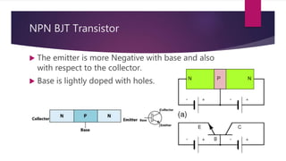
NPN BJT Transistor
ļµThe emitter is more Negative with base and also
with respect to the collector.
ļµ Base is lightly doped with holes.
13.
PNP BJT Transistor
ļµThe emitter is more Positive with base and also with
respect to the collector.
ļµ Base is lightly doped with electrons.
14.
CONSTRUCTION (NPN)
⢠THEBIPOLAR JUNCTION TRANSISTOR (NPN) THREE LAYER
SEMICONDUCTOR SANDWICH WITH
AN EMITTER AND COLLECTOR AT THE ENDS, AND A BASE IN
BETWEEN.
⢠THE KEY TO THE FABRICATION OF A BIPOLAR JUNCTION
TRANSISTOR IS TO MAKE THE MIDDLE LAYER, THE BASE, AS THIN
AS POSSIBLE WITHOUT SHORTING THE OUTSIDE LAYERS ā THE
EMITTER AND THE COLLECTOR.
⢠THE EMITTER IS HEAVILY DOPED WITH ELECTRONS, BASE IS
LIGHTLY DOPED WITH HOLES AND COLLECTOR IS MODERATELY
15.
WORKING(NPN)
ļ” The transistoris in OFF state when the base voltage is same as the
emitter voltage. The transistor mode is in ON state when the base
voltage decreases with respect to the emitter.
ļ” To Operate BJT in Active region, BE junction is made forward bias
and the CB is made reverse bias junction.
Advantages of BiCMOStechnology
⢠Analog amplifier design is facilitated and improved by using high
impedance CMOS circuit as input and remaining are realized by using
bipolar transistors.
⢠BiCMOS is essentially vigorous to temperature and process variations
offering good economical considerations (high percentage of prime units)
with less variability in electrical parameters.
⢠High load current sinking and sourcing can be provided by BiCMOS devices
as per requirement.
⢠Since it is a grouping of bipolar and CMOS technologies we can use BJT if
speed is a critical parameter and we can use MOS if power is a critical
parameter and it can drive high capacitance loads with reduced cycle time.
21.
⢠It haslow power dissipation than bipolar technology alone.
⢠This technology found frequent applications in analog power
managing circuits and amplifier circuits such as BiCMOS amplifier.
⢠It is well appropriate for input/ouput intensive applications, offers
flexible inputs/outputs (TTL, CMOS and ECL).
⢠It has the advantage of improved speed performance compared to
CMOS technology alone.
⢠Latch up invulnerability.
⢠It has the bidirectional capability (source and drain can be
interchanged as per requirement).
22.
Drawbacks of BiCMOStechnology
⢠The fabrication process of this technology is comprised of both the
CMOS and bipolar technologies increasing the complexity.
⢠Due to increase in the complexity of the fabrication process, the cost
of fabrication also increases.
⢠As there are more devices, hence, less lithography.
23.
BiCMOS technology andApplications
⢠It can be analyzed as AND function of high density and speed.
⢠This technology is used as an alternate of the previous bipolar, ECL
and CMOS in the market.
⢠In some applications (in which there is finite budget for power) the
BiCMOS speed performance is better than the that of bipolar.
⢠This technology is well suited for the intensive input/output
applications.
⢠The applications of BiCMOS were initially in RISC microprocessors
rather than traditional CISC microprocessors.
24.
⢠This technologyexcels its applications, mainly in two areas of
microprocessors such as memory and input/output.
⢠It has a number of applications in analog and digital systems, resulting in
the single chip spanning the analog-digital boundary.
⢠It overpass the gap permitting course of action and circuit margins to be
crossed.
⢠It can be used for sample and hold applications as it provides high
impedance inputs.
⢠This is also used in applications such as adders, mixers, ADC and DAC.
⢠To conquer the limitations of bipolar and CMOS operational amplifiers the
BiCMOS processes are used in designing the operational amplifiers. In
Operational amplifiers, high gain and high frequency characteristics are
desired. All these desired characteristics can be gained by using these
BiCMOS amplifiers.
#4Ā Glue Logic is a special form of digital circuitry that allows different types ofĀ logicĀ chips or circuits to work together by acting as an interface between them.Ā