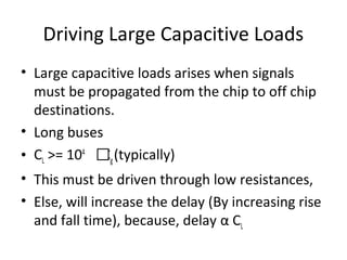
This document discusses different techniques for driving large capacitive loads:
1. Cascading inverters as drivers, with an optimal fan-out of 3 inverters for a 1um technology.
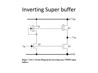
2. Super buffers, which use an inverting buffer with 4 transistors and a non-inverting buffer to quickly charge and discharge large loads.
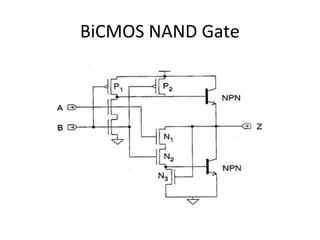
3. BiCMOS drivers, which combine BJT and CMOS transistors to drive loads faster than standard CMOS alone. The document provides circuit diagrams of BiCMOS inverters and NAND gates.