This document provides course materials for the subject EC3552 VLSI and Chip Design, including the course objectives, 5 units of study, expected course outcomes, and references. The 5 units cover MOS transistor principles, combinational logic circuits, sequential logic circuits and clocking strategies, memory architecture and arithmetic circuits, and ASIC design and testing. Key concepts include MOSFET characteristics, static and dynamic CMOS design, latches and registers, interconnect modeling, and the ASIC design flow. The course aims to provide an in-depth understanding of IC technology components, logic circuit design principles, memory architectures, and the chip design process.


![10
.
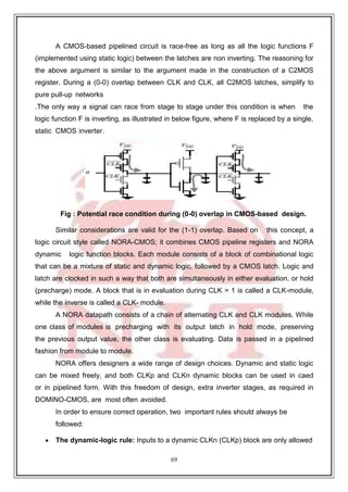
ps + Vsb - 𝜑 s
Vgs = 1.8
Vgs = 1.5
Vgs
= 1.2
Vgs = 0.9
Vgs = 0.6
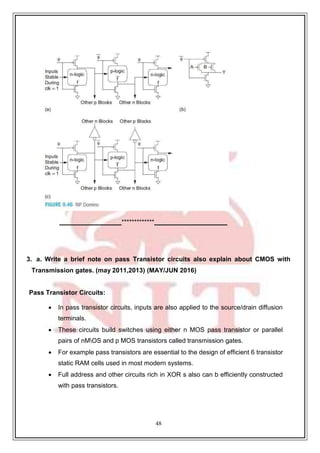
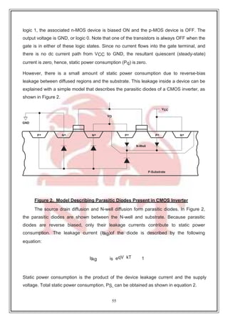
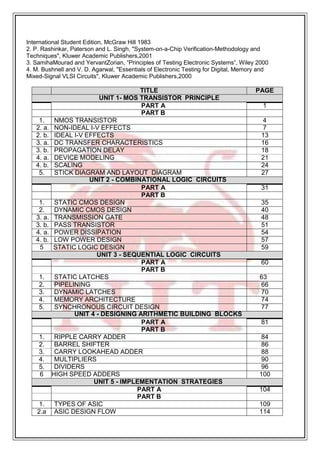
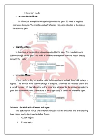
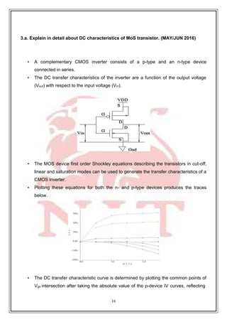
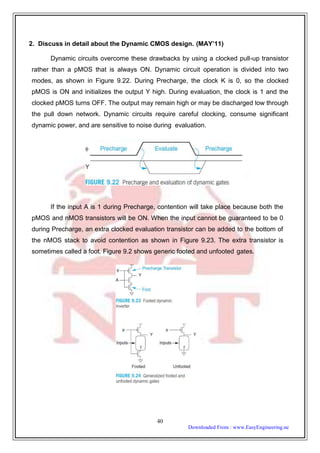
Imagine that the source voltage is close to the body voltage. Increasing Vds
decreases the effective channel length. Shorter length results in higher
current. Thus Ids increases with Vds in saturation as shown below.
In saturation region
Where 𝜆 = Channel length modulation factor
Ids
(A)
400
300
200
100
Body Effect:
0
0 0.3 0.6 0.9 1.2 1.5 1.8 Vds
Transistor has four terminals named gate, source, drain and body. The potential difference
between the source and body Vsb affects the threshold voltage.
Vt = Vto + ᴕ ( )
Where
Vto = Threshold Voltage when the source is at the body potential
𝜑 s = Surface Potential at threshold = 2vT ln Nd
Ni
Vsb = Potential difference between the source and body.
Sub threshold condition:
Ideally current flows from source to drain when Vgs > V t. In real transistor,
current does not abrupthy cut off below threshold, but rather drops off
exponentially as
Ids = I dso e Vgs - V t [ 1- e V ds]
nvt Vt .
This is also called as leakage and often thias results in underired current when a
transistor is normally OFF. Idso is the current at thresholo and is dependent on process and
device geometry
Applications:-
This is used in very low power analog circui
This is used in dynamic circuits and OR AM
Advantage:
1) Leakage increases exponentially as Vt decreases or as temperature rises.
Disadvantages:
Ids = 𝛽 (Vgs - V t)2 (1+ 𝜆 V ds
2](https://image.slidesharecdn.com/vlsinotes-240322092828-aa8658a6/85/VLSI-NOTES-docx-notes-for-vlsi-ece-deptmnt-14-320.jpg)
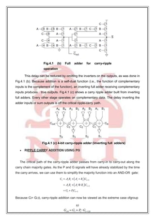
![1
1
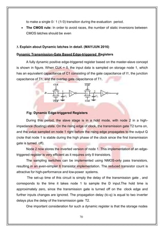
p substrate
n well
n+
p+
p+
n+
n+
p+
1) It becomes worse by drain induced barrier lowering in which a positive Vds
effectively reduces Vt. This effect is especially pronounced in short channel
transistors.
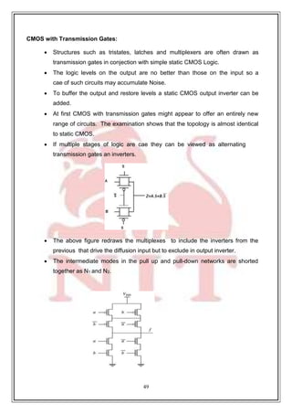
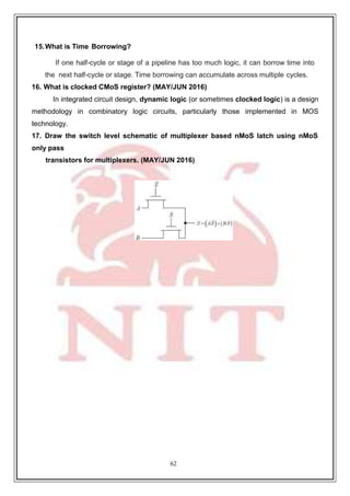
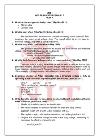
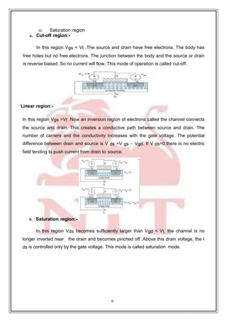
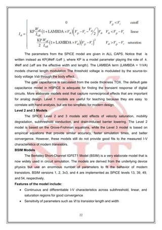
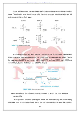
Junction Leakage:
The P-n junction between diffusion and the substrate or well form diodes are
shown below.
The substrate and well are tied to GND or VDD to ensure that these diodes
remain reverse biased.
The reverse biased diodes still conduct a small amount of current I o.
ID = Is [ e VD -1]
VT
Where
ID = diode current
Is = diode reverse- biased saturation current that depends on doping levels and on
the area and perimeter of the diffusion region.
Tunneling :
Based on quantum mechanics, we see that the is a finite probability that carriers will
tunnel through the gate oxide. This results in gate leakage current flowing into the gate.
The probability of tunnelling drops off exponentially with oxide thickness.
Large tunnelling currents impact not only dynamic nodes but also quiescent
power consumption and thus may limit oxide thickness tor.
Tunnelling can purposely be used to create electrically erasable memory
devices. Different dielectrics may have different tunneting properties.
Temperature Dependance:
Temperature influences the characteristics of transistors. Carrier mobility decreases
with temperature.
𝜇 (T) = 𝜇 (Tr ) ( T ) -k
𝜇
Tr](https://image.slidesharecdn.com/vlsinotes-240322092828-aa8658a6/85/VLSI-NOTES-docx-notes-for-vlsi-ece-deptmnt-15-320.jpg)


![2
1
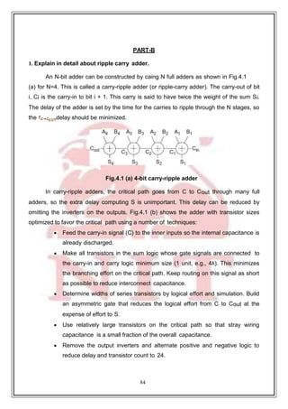
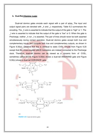
Delay in multistage logic networks:
Logical effort is independent of size and electrical effort is dependent
on size.
1. path logical effort
2. path electrical effort
3. path effort
4. branching effort
5. path branching effort
6. path delay
7. minimum possible delay
Choosing the best number of stages:
Inverters can be added at the end of a path without changing its function. Extra
inverters and parasitic delay, but do not change the path logical effort.
4.a. Explain about device modeling in detail.(MAY/JUN 2012)(MAY/JUN 2013).
SPICE provides a wide variety of MOS transistor models with various trade-offs
between complexity and accuracy. Level 1 and Level 3 models were historically important,
but they are no longer adequate to accurately model very small modern transistors. BSIM
models are more accurate and are presently the most widely used. Some companies use
their own proprietary models. This section briefly describes the main features of each of
these models. It also describes how to model diffusion capacitance and how to run
simulations in various process corners. The model descriptions are intended only as an
overview of the capabilities and limitations of the models; refer to a SPICE manual for a
much more detailed description if one is necessary.
Level 1 Models
The SPICE Level 1, or Shichman-Hodges Model [Shichman68] is closely related to the
Shockley model described in EQ (2.10), enhanced with channel length modulation and the
body effect. The basic current model is:](https://image.slidesharecdn.com/vlsinotes-240322092828-aa8658a6/85/VLSI-NOTES-docx-notes-for-vlsi-ece-deptmnt-25-320.jpg)


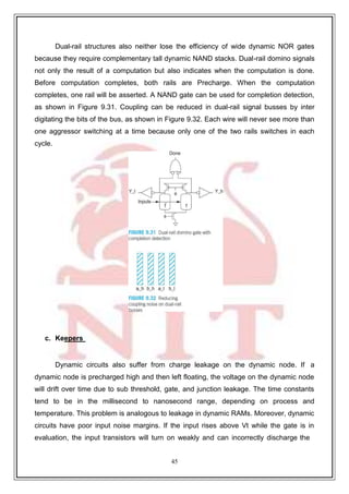
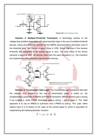
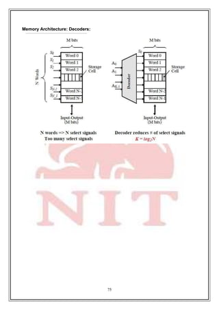
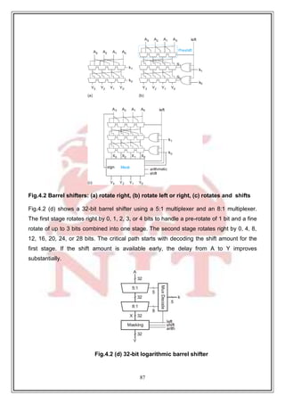
![46
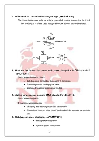
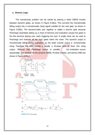
output. Both leakage and noise margin problems can be addressed by adding a keeper
circuit. Figure 9.33 shows a conventional keeper on a domino buffer. The keeper is a
weak transistor that holds, or staticizes, the output at the correct level when it would
otherwise float. When the dynamic node X is high, the output Y is low and the keeper is
ON to pre- vent X from floating. When X falls, the keeper initially opposes the transition so
it must be much weaker than the pull down network. Eventually Y rises, turning the
keeper OFF and avoiding static power dissipation.
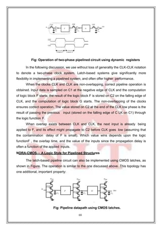
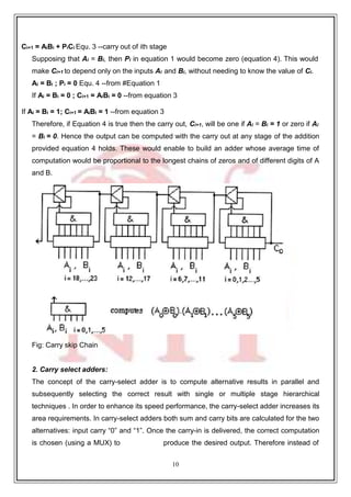
d. Multiple-Output Domino Logic (MODL)
It is often necessary to compute multiple functions where one is a
subfunction of another or shares a subfunction. Multiple-output domino logic
(MODL) [Hwang89, Wang97] saves area by combining all of the computations
into a multiple-output gate. A popular application is in addition, where the carry-out
ci of each bit of a 4-bit block must be computed, as discussed in Section 11.2.2.2.
Each bit position i in the block can either propagate the carry (pi) or generate a
carry (gi). The carry-out logic is
This can be implemented in four compound AOI gates, as shown in Figure](https://image.slidesharecdn.com/vlsinotes-240322092828-aa8658a6/85/VLSI-NOTES-docx-notes-for-vlsi-ece-deptmnt-50-320.jpg)