Downloaded 216 times

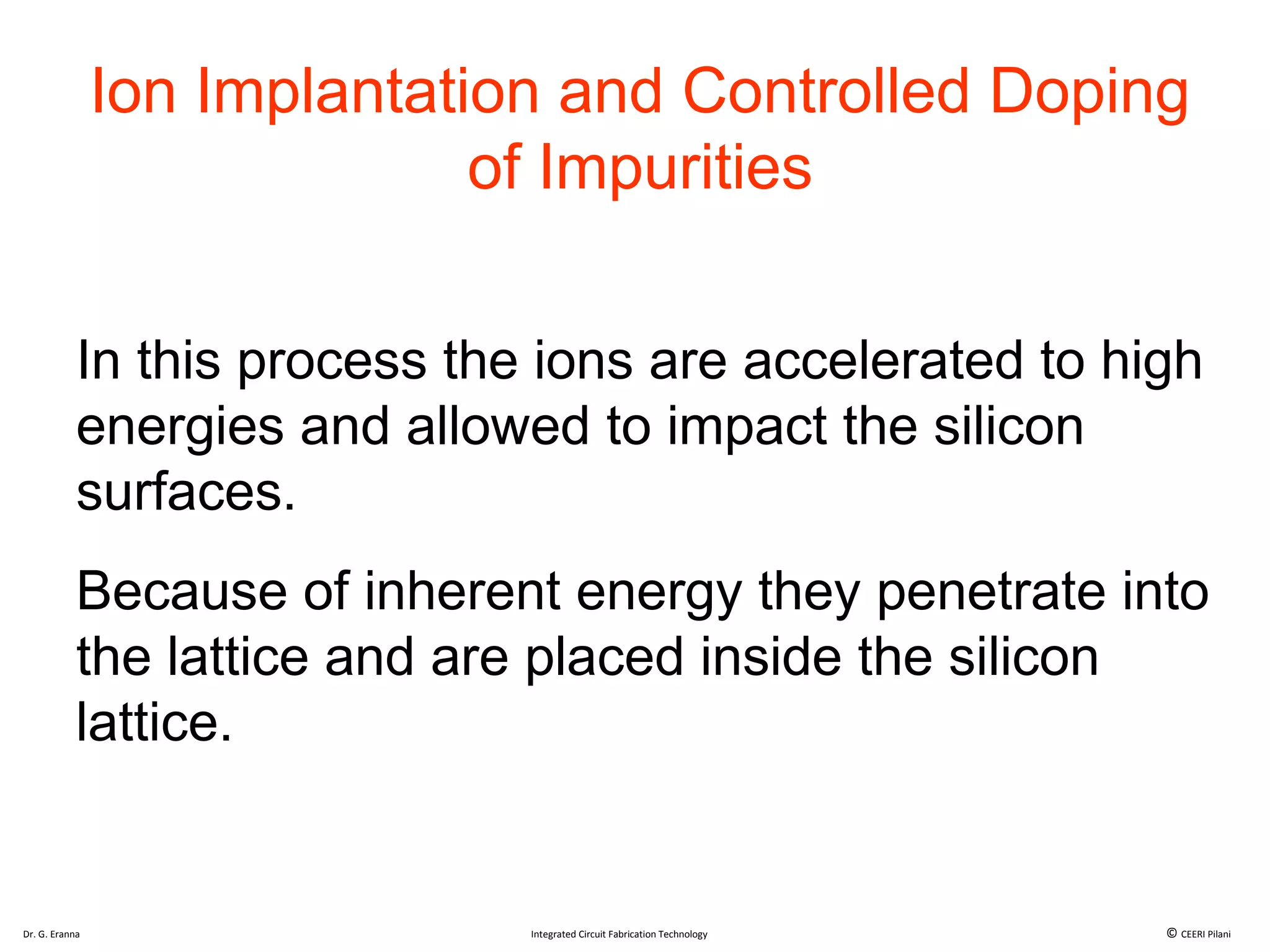
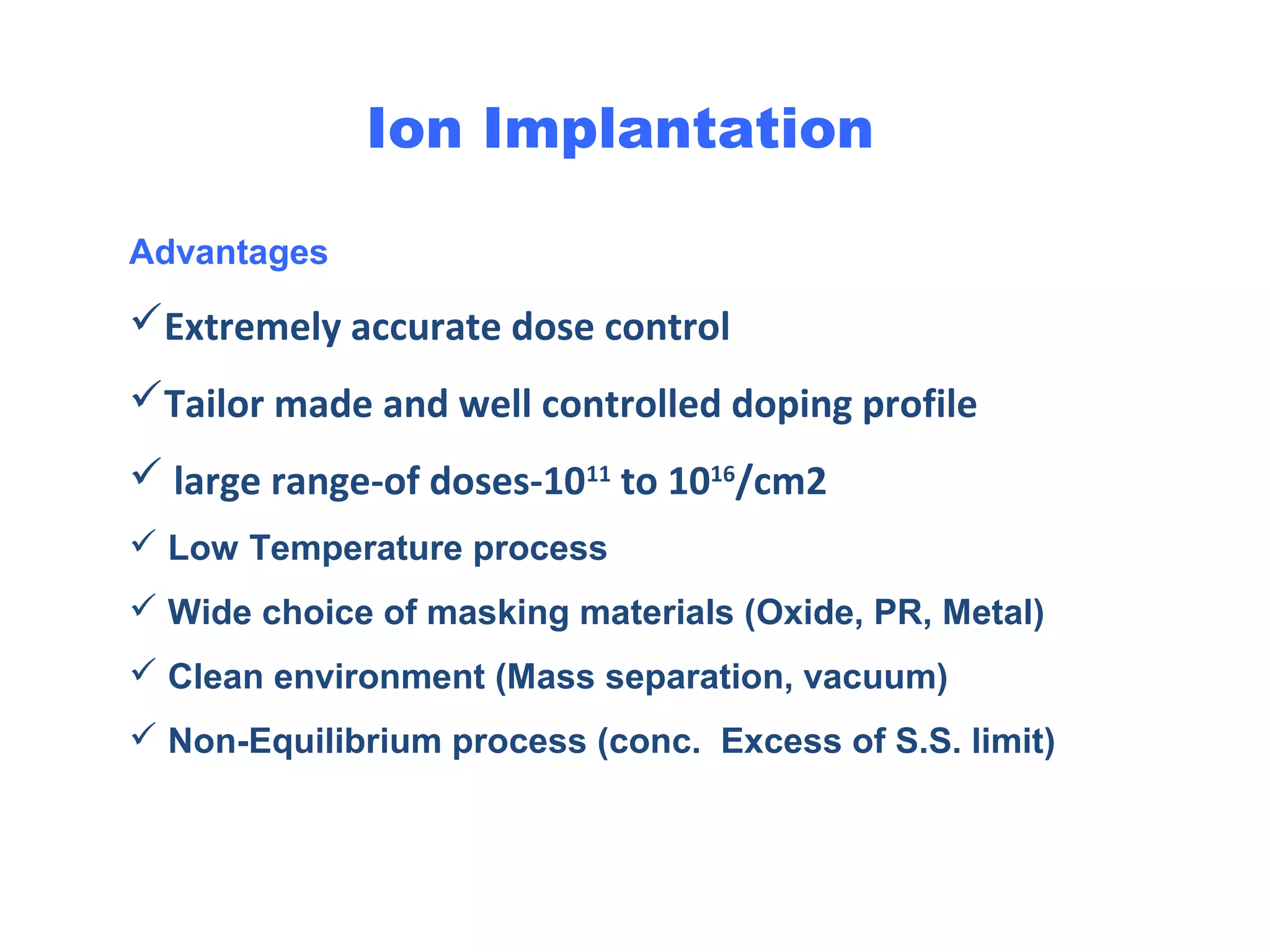
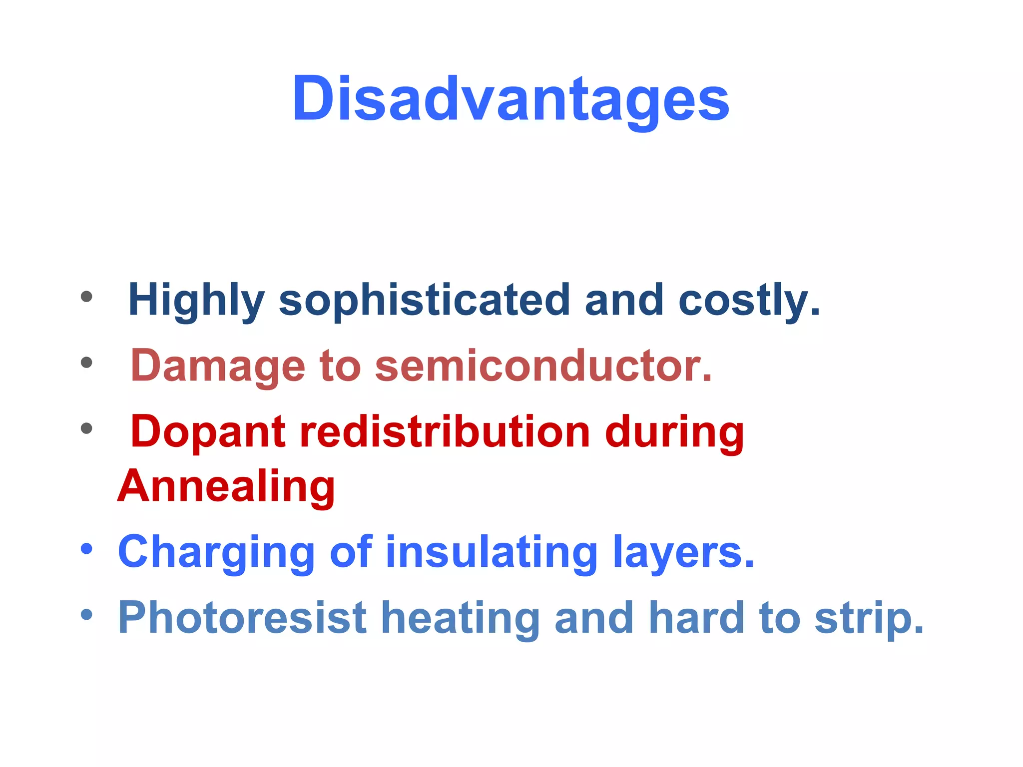
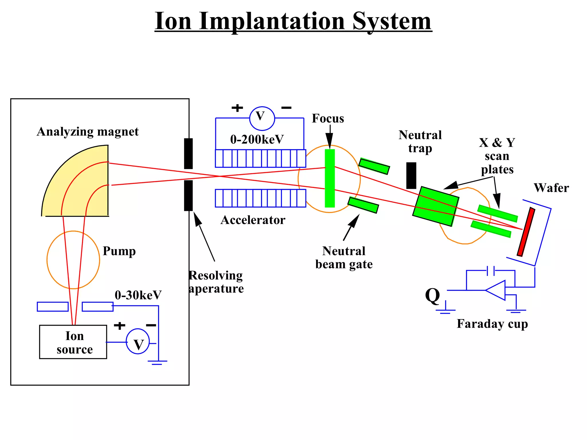
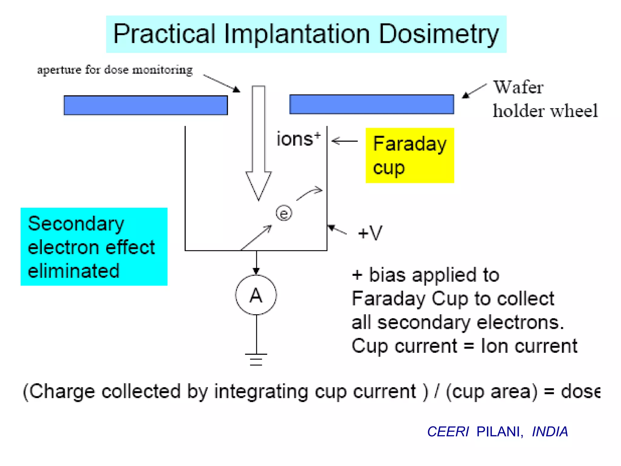

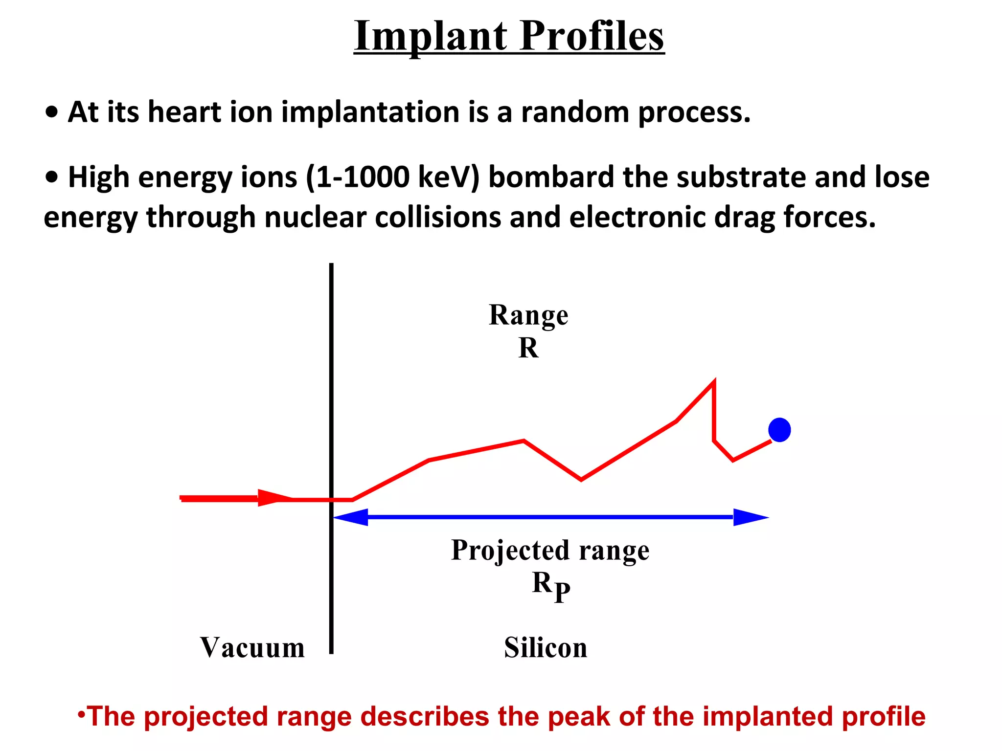

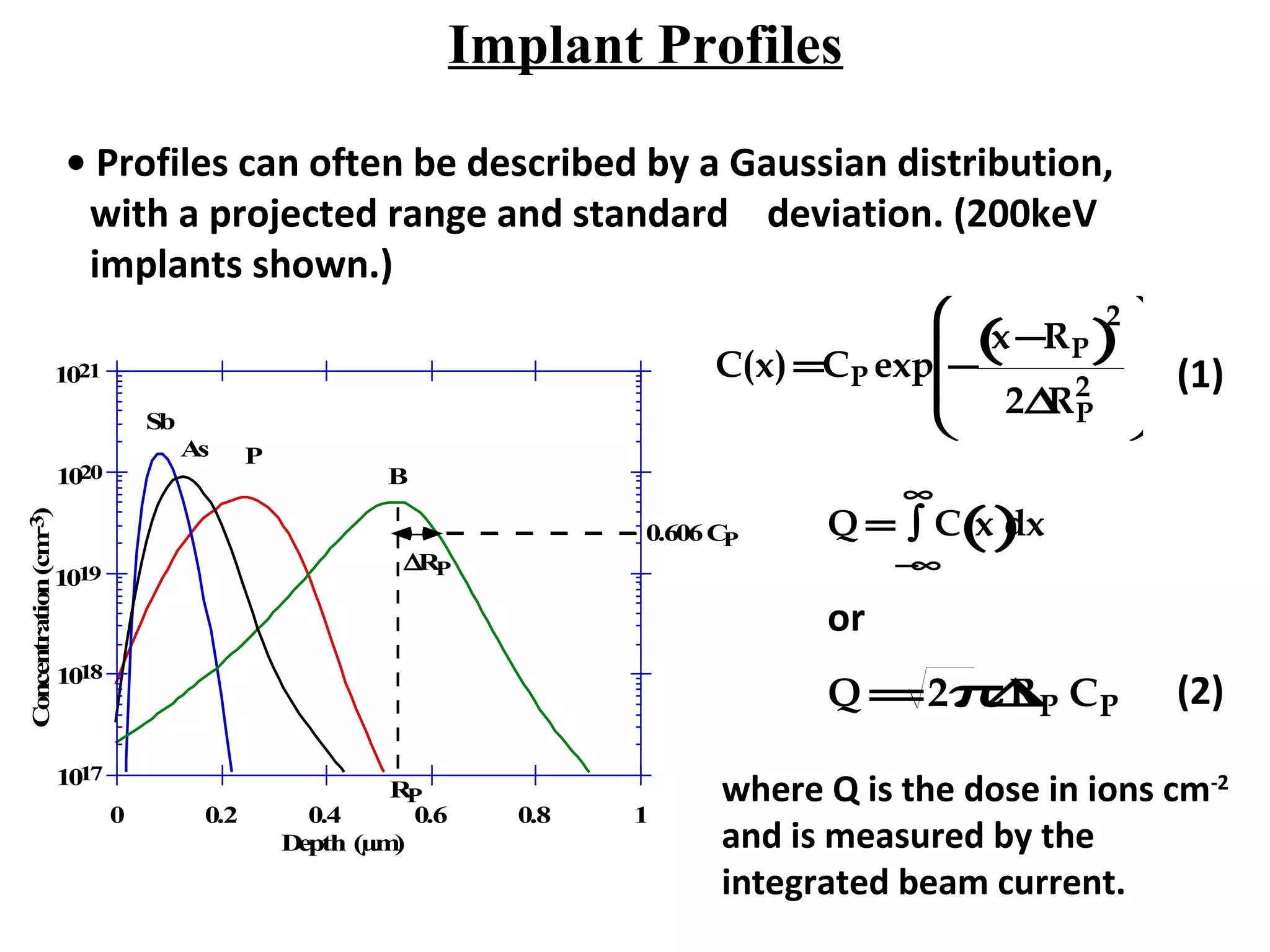
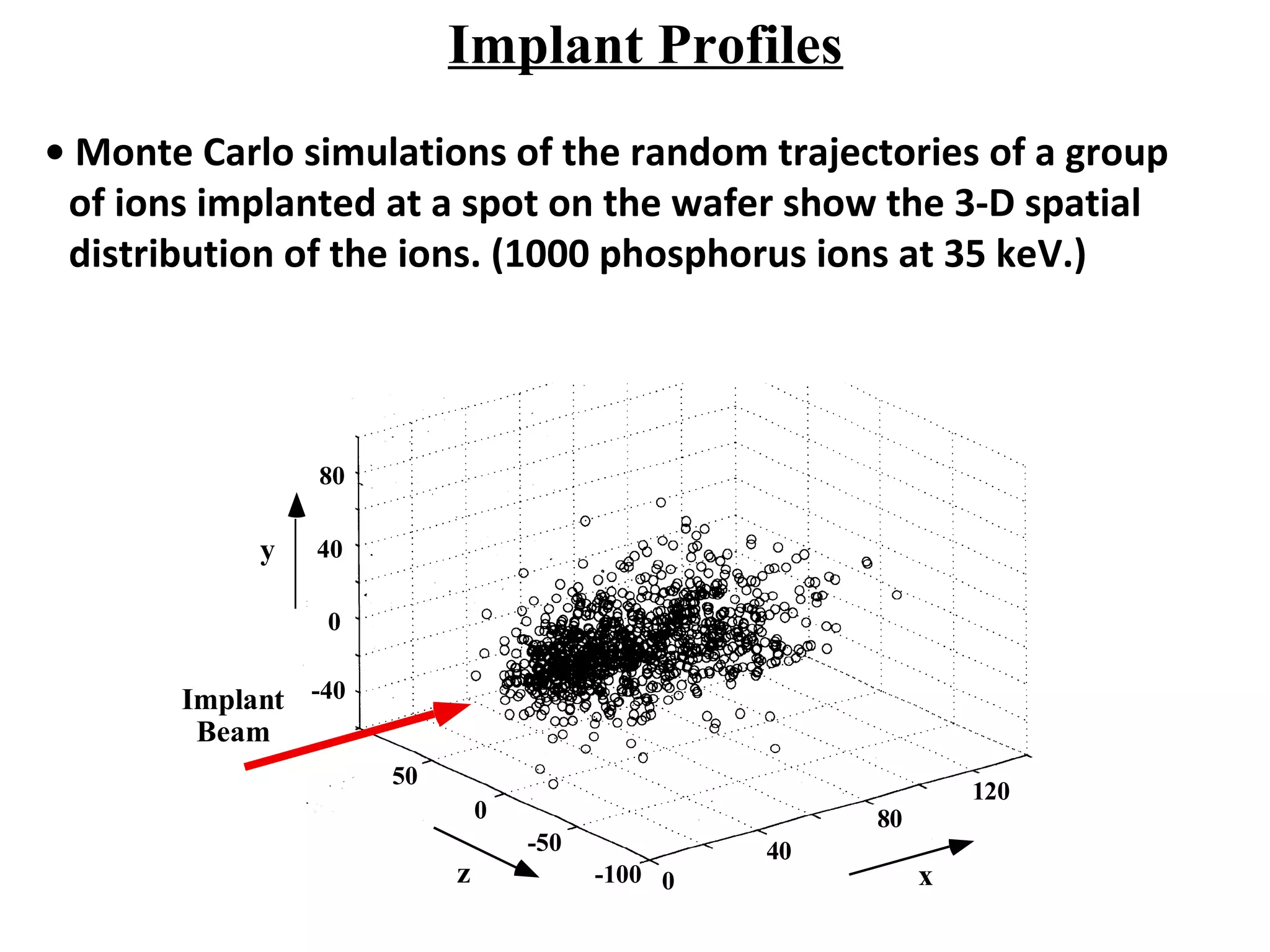
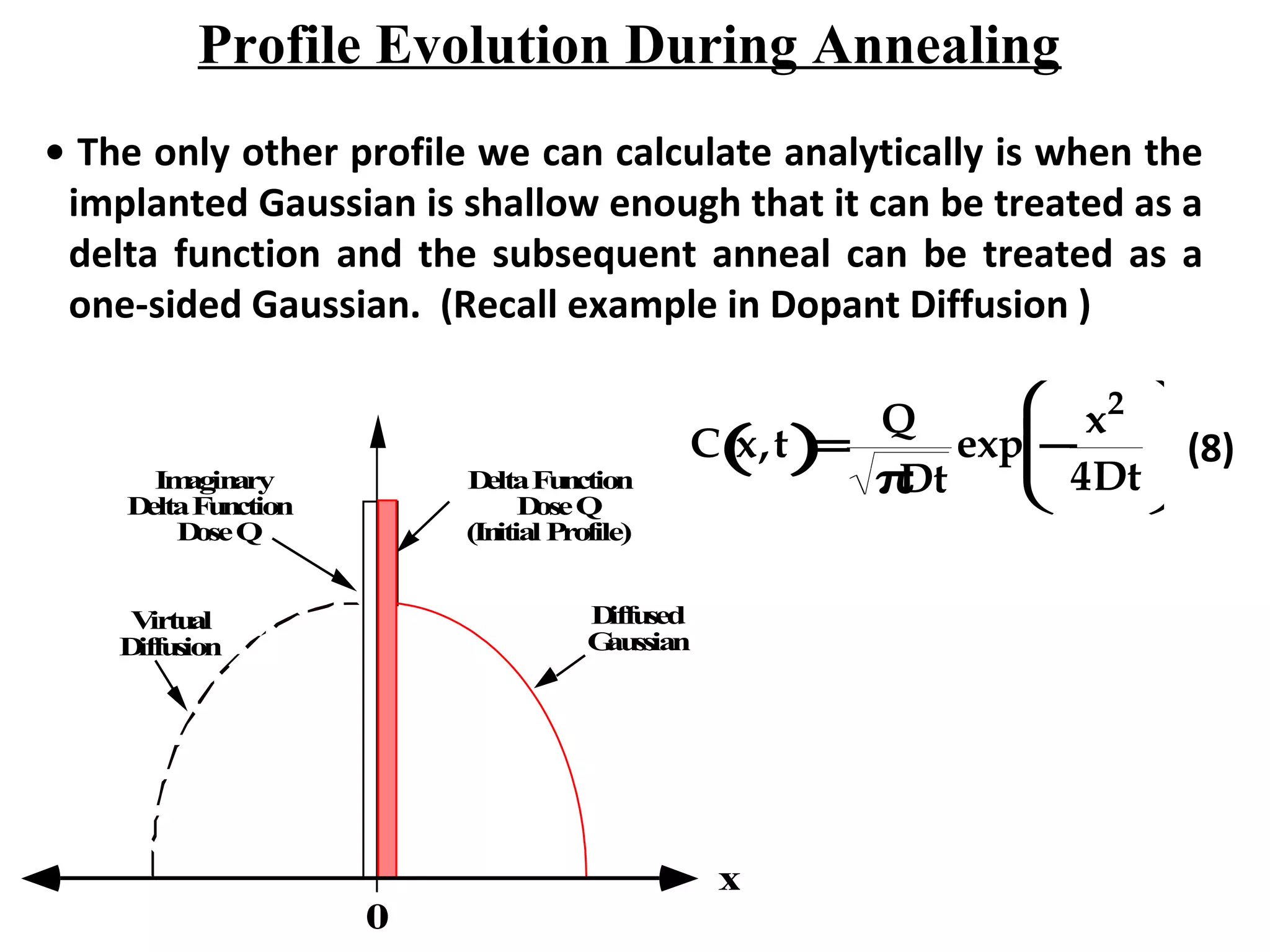
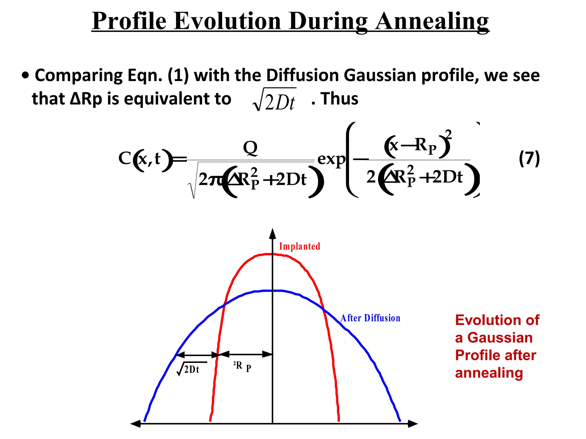
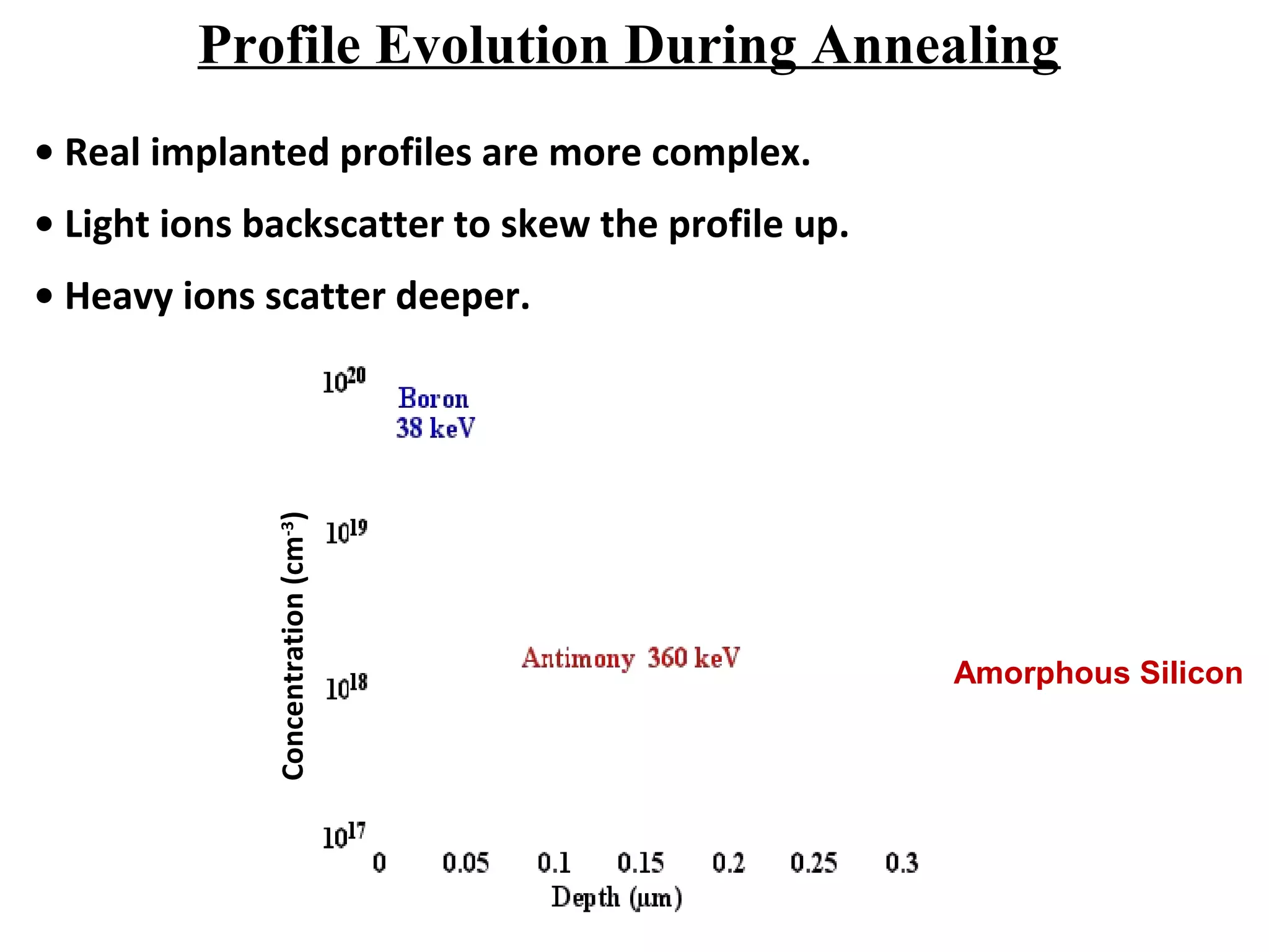
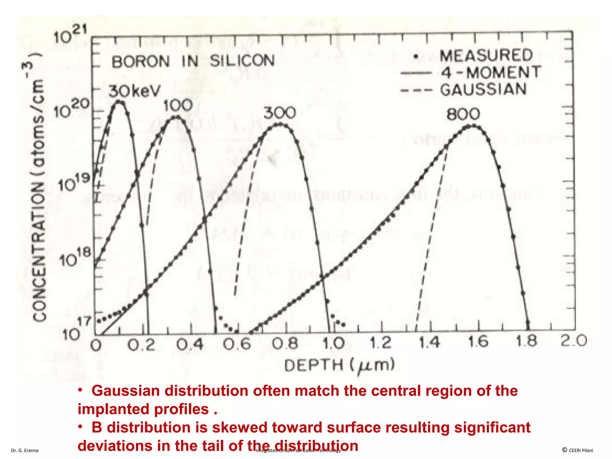
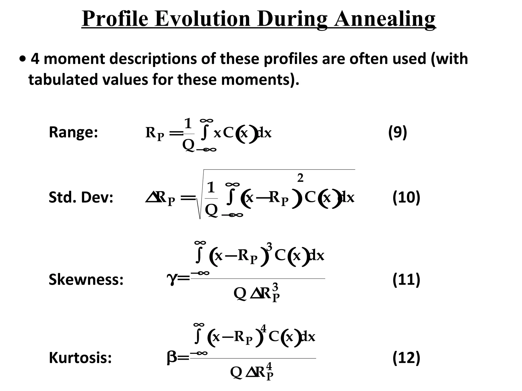
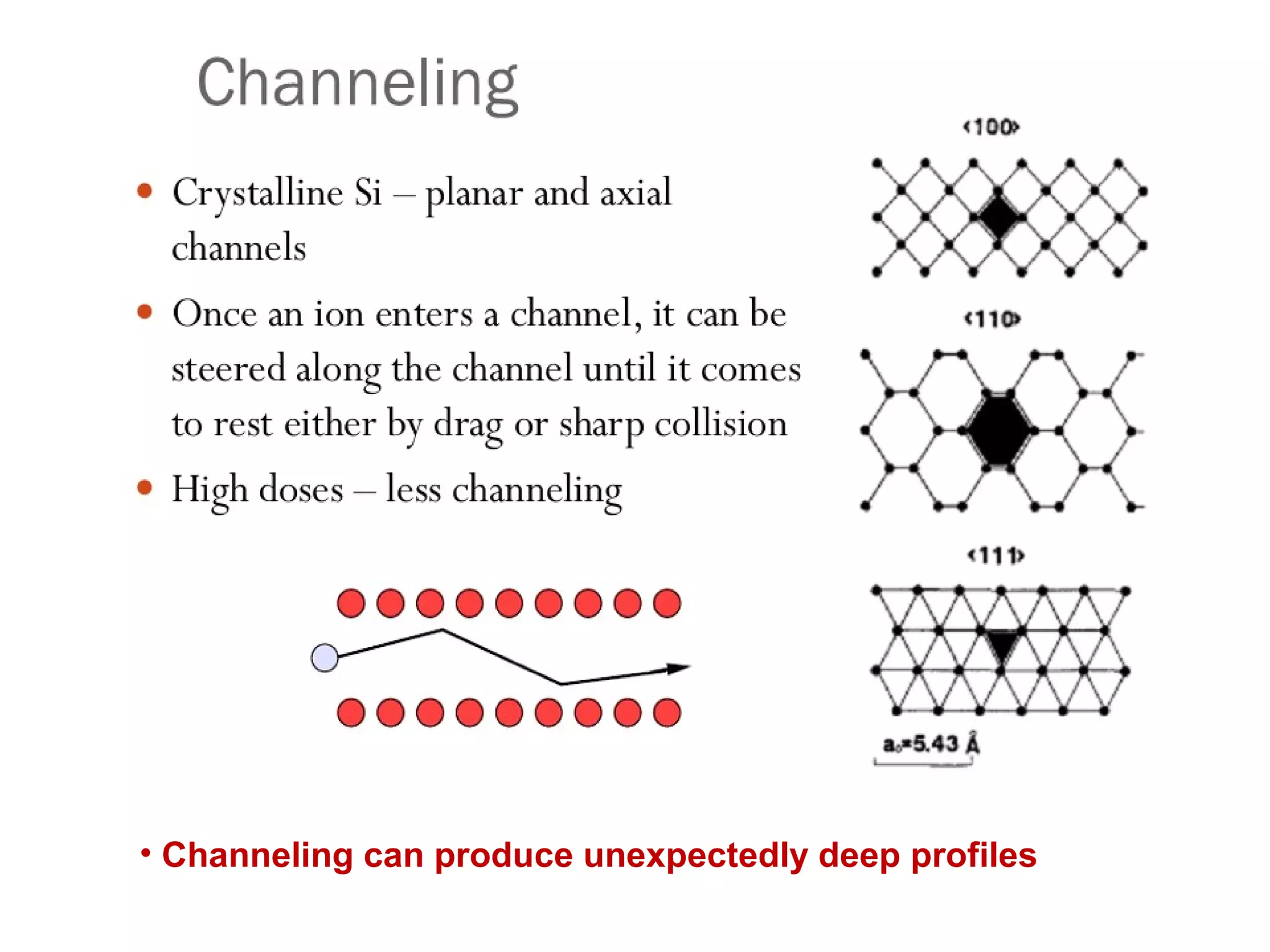
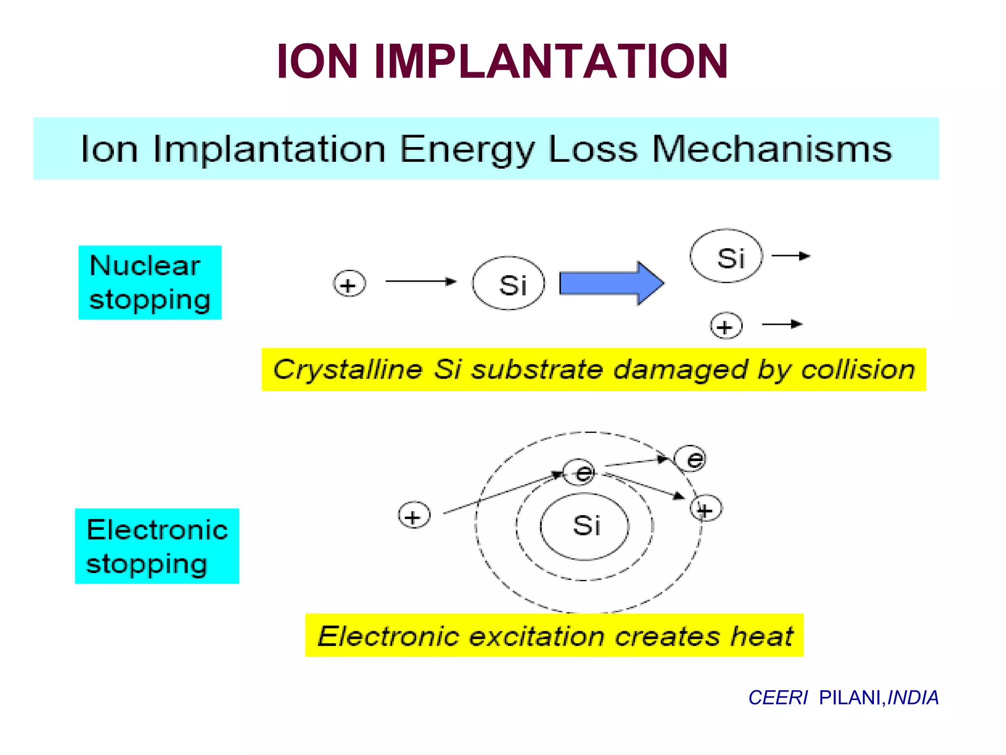


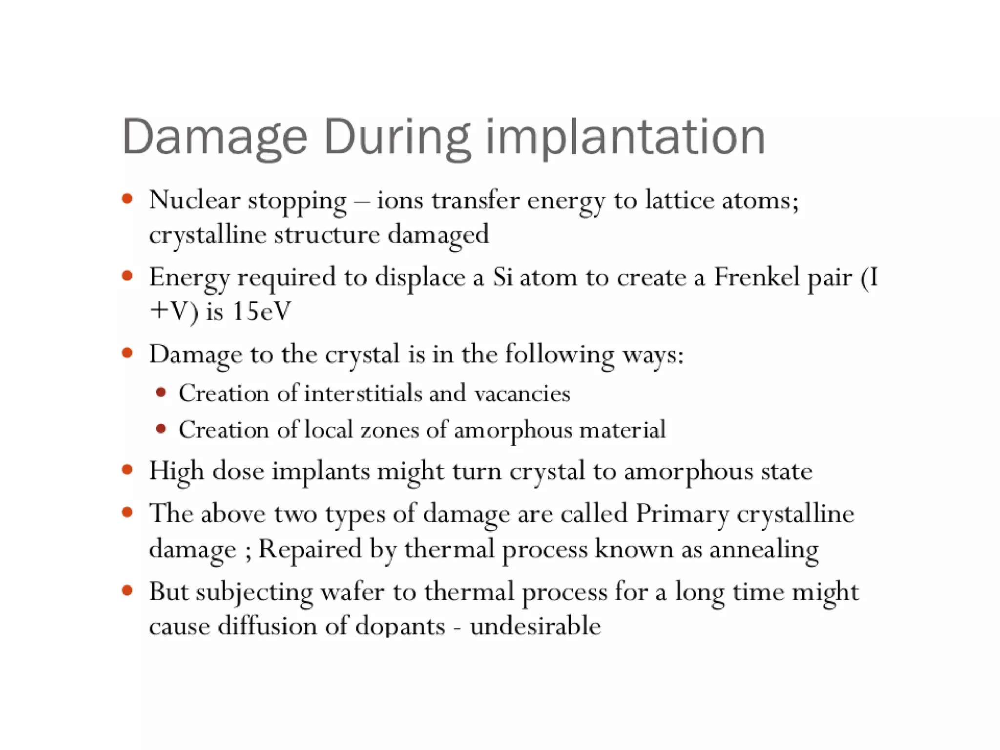


Ion implantation is a process used to introduce impurity atoms into a crystalline substrate to modify its electronic properties. Ions are accelerated to high energies and bombard the silicon surface, penetrating the lattice and becoming embedded. It allows for extremely accurate control of the dopant dose and distribution. However, it is a complex process that can damage the semiconductor and require annealing. The distribution of implanted ions is typically Gaussian but is affected by backscattering and channeling effects. During annealing, the profile will diffuse but the initial profile complexity must be properly modeled.


