Download as PDF, PPTX
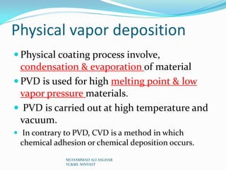
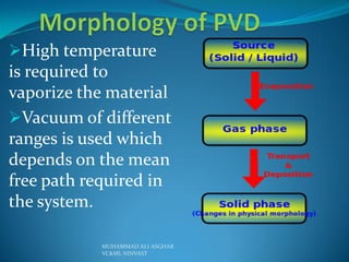
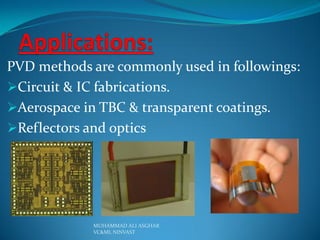

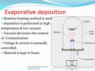
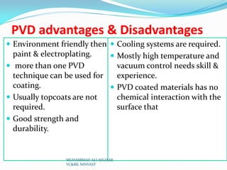


Physical vapor deposition (PVD) involves evaporating or sputtering material in vacuum chambers to form thin films or coatings on surfaces. Different PVD techniques include evaporative deposition using resistive heating or electron beams, sputter deposition using plasma or ion beams, and pulsed laser deposition. PVD is commonly used for circuit fabrication, aerospace coatings, and optics due to its ability to deposit thin, uniform coatings of various materials at high temperatures and precise thicknesses. Some advantages of PVD include producing environmentally friendly coatings without requiring post-deposition treatments, while disadvantages include high energy and vacuum requirements.


![Thin_Film_Technology_introduction[1]](https://cdn.slidesharecdn.com/ss_thumbnails/1b4496c8-2102-411b-8465-a3dd3f398327-150205034538-conversion-gate02-thumbnail.jpg?width=640&height=640&fit=bounds)


![Thin Film Deposition techniques [Autosaved].pptx](https://cdn.slidesharecdn.com/ss_thumbnails/thinfilmdepositionautosaved-241117063353-54857e32-thumbnail.jpg?width=640&height=640&fit=bounds)


![5G Explained! A High Level Overview [Introduction]](https://cdn.slidesharecdn.com/ss_thumbnails/5gexplainedahighleveloverview-260119165306-cc137a3e-thumbnail.jpg?width=640&height=640&fit=bounds)


