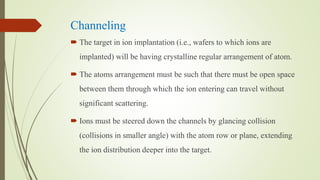
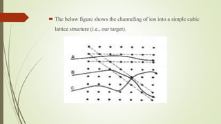
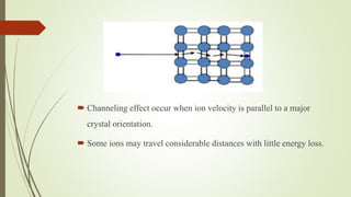
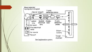
Ion implantation is a process used to dope semiconductors by accelerating ions of the desired impurity towards the target wafer. The impurity ions are implanted near the surface in a Gaussian distribution profile. The penetration depth and dose of impurities can be tightly controlled. Channeling can occur if ions are aligned with the crystal structure, allowing deeper implantation. Ion implantation offers precise doping control and can be done at low temperatures, but the equipment is expensive and lattice damage can occur. It is commonly used in semiconductor device fabrication.


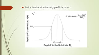
![Impurity distribution of implanted ions
The distribution of implanted ions as a function of distance x from
the silicon surface will be a Gaussian distribution given by
𝑁 𝑥 = 𝑁𝑝 𝑒𝑥𝑝 [
−(𝑥−𝑅𝑝)²
2∆𝑅𝑝²
]
𝑁𝑝 = Peak concentration of implanted ion
𝑅𝑝 = Projected range
𝑥 = Distance into substrate from surface
∆𝑅𝑝 = standard deviation of projected range](https://image.slidesharecdn.com/ionimplantation-210221133632/85/Ion-implantation-7-320.jpg)
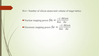
![Stopping power
When an energetic ion enters a solid, it losses energy.
The energy loss in the target mainly due to two mechanisms.
Ion-electron interaction [Electronic stopping power]
Ion-nucleus interaction [Nuclear stopping power]
Let 𝐸𝑖𝑜𝑛 = Energy of bombarding ion](https://image.slidesharecdn.com/ionimplantation-210221133632/85/Ion-implantation-10-320.jpg)