Download as PDF, PPTX

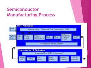

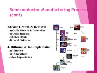


The document outlines the semiconductor manufacturing process, detailing historical milestones and various techniques involved, such as silicon manufacturing, photolithography, and diffusion. It describes methods including the Czochralski technique for crystal growth, the application of photolithography for patterning, and the oxidation and etching processes required for creating integrated circuits. Additionally, it compares diffusion and ion implantation methods for doping silicon, highlighting their advantages and limitations.


