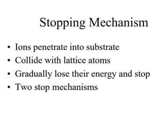
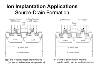
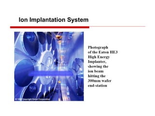
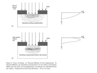
1. Ion implantation involves ionizing dopant atoms, accelerating them into a beam, and embedding them into a wafer's crystalline structure. This allows for precise doping control without high temperatures.
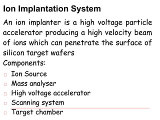
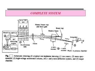
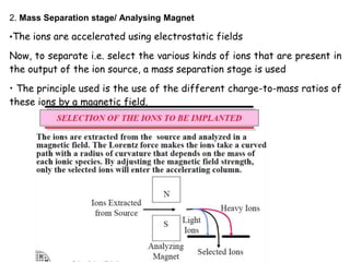
2. An ion implanter consists of an ion source, mass analyzer, accelerator, and target chamber. The ion source produces dopant ions which the mass analyzer selects before acceleration into the target wafer.
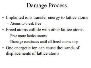
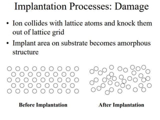
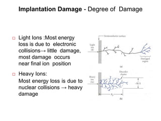
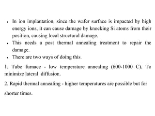
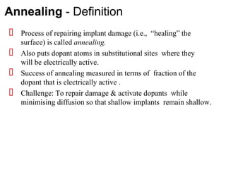
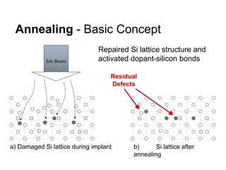
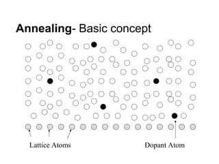
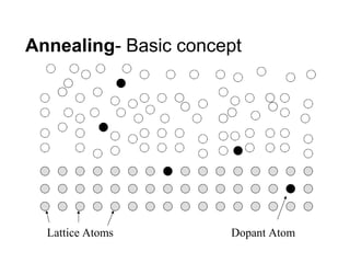
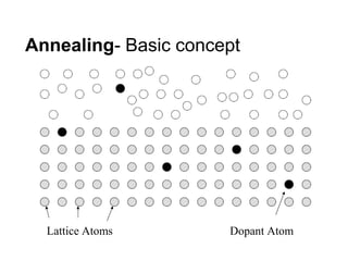
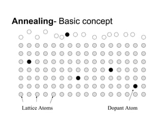
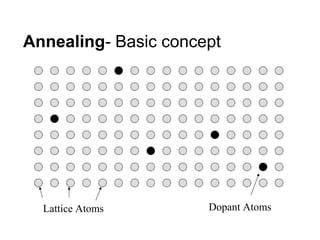
3. Implanted ions can damage the wafer's crystal structure, requiring subsequent annealing to activate the dopants and repair damage. Precise annealing is needed to minimize dopant diffusion.


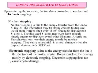
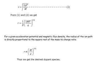
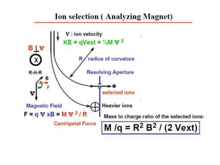
![● The magnetic field of the analyzer is chosen such that only ions
with the desired charge to mass ratio can travel through
without being blocked by the analyzer walls.
● A magnetic field B is applied normal to the path of ions with
charge q and velocity v
● The force on the ions is given by F=qvB and the ions move in a
circular path of radius r and there is a centripetal force
F=M v2/R
● Therefore, qvB= M v2/R [velocity v is unchanged]
And R = Mv/qB ------------------------------------(1)
● Now for an ion accelerated through a potential Vext the velocity
is given by:
M v2 /2 = qVex , from where we get v as:](https://image.slidesharecdn.com/ionimplantation1-220724175850-48dd11b3/85/IONIMPLANTATION-1-pptx-13-320.jpg)
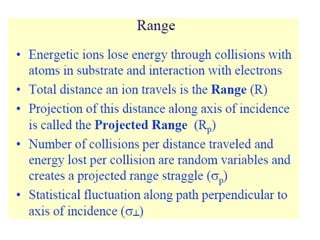
![Most semiconductors are crystalline and have highly anisotropic properties. Because of the
ordered arrangement of lattice atoms, ions can penetrate more deeply into the crystal along
major axis and planes. This phenomenon is called channeling effect. To avoid channeling,
ion implantation is often carried out with an ion beam misoriented from the major axis by an
angle of at least 7 to 10 . Both Si and GaAs behave nearly as an amorphous solid when a
misoriented beam is used.
Channeling Effect
Fig. channeling effect
Ref-IcengB1
Ref pdf : implant-2[1]
Not isotropic.
= Having propertiesthat differ according to the direction of
measurement.
amorphous solid=A noncrystalline solid with nowell-defined
ordered structure.](https://image.slidesharecdn.com/ionimplantation1-220724175850-48dd11b3/85/IONIMPLANTATION-1-pptx-20-320.jpg)