Downloaded 304 times

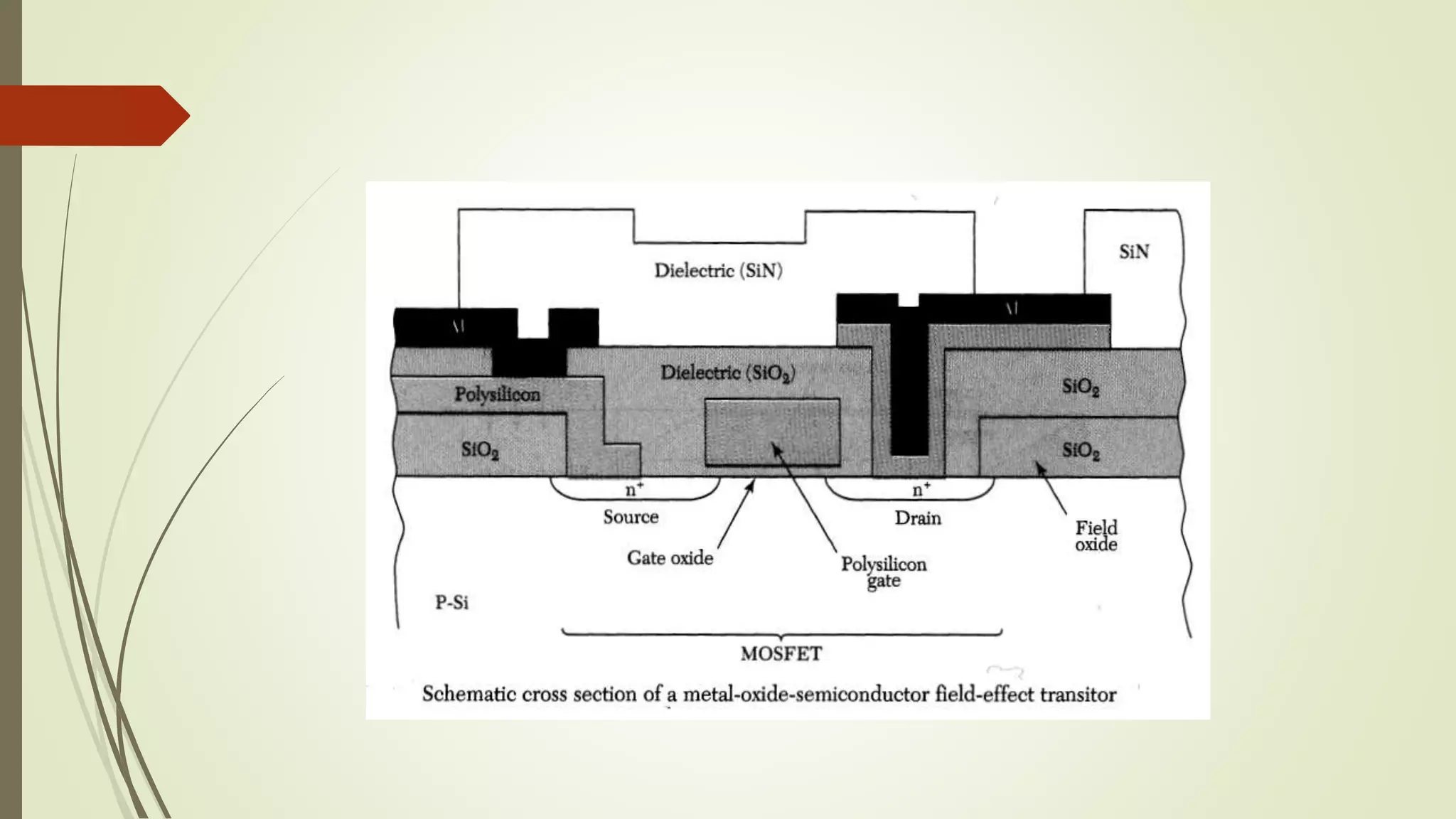
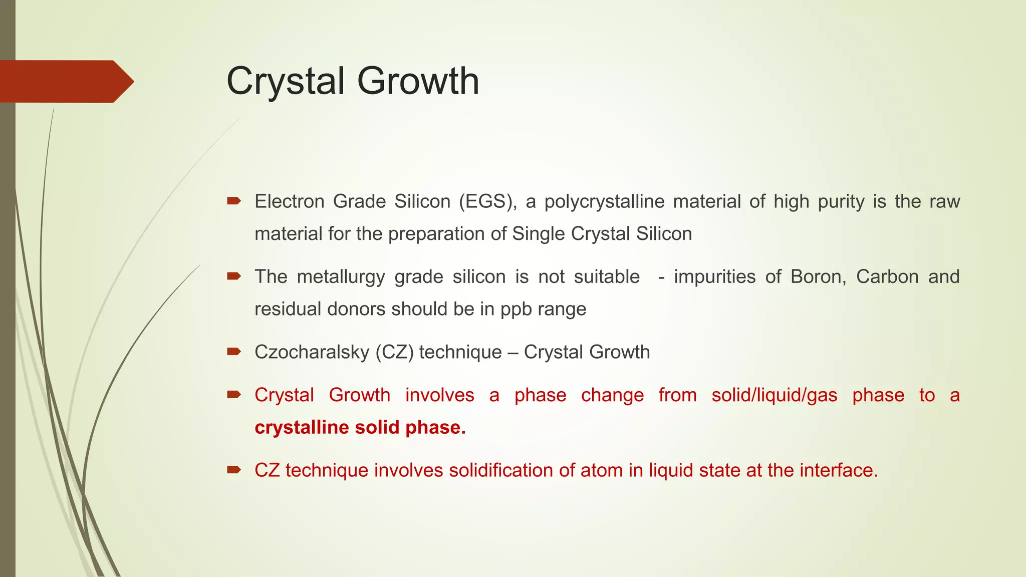
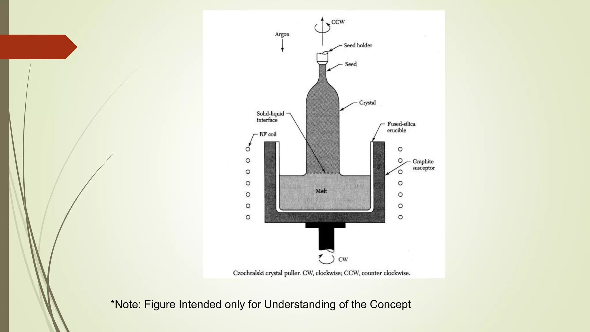
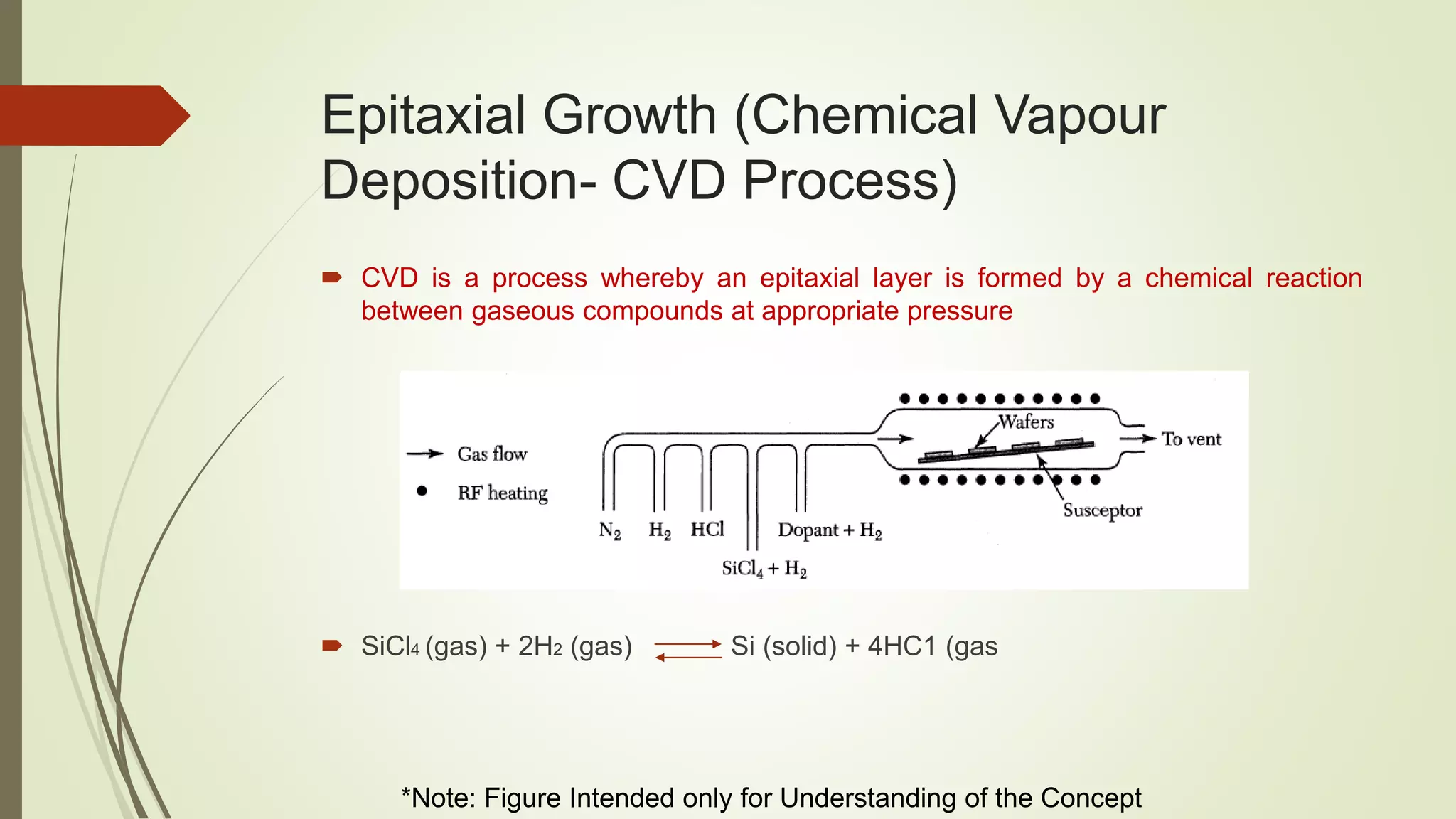
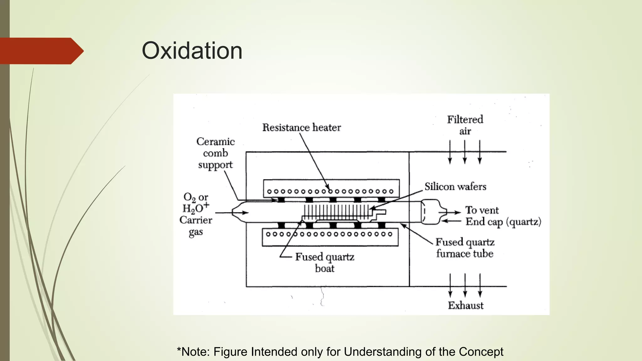
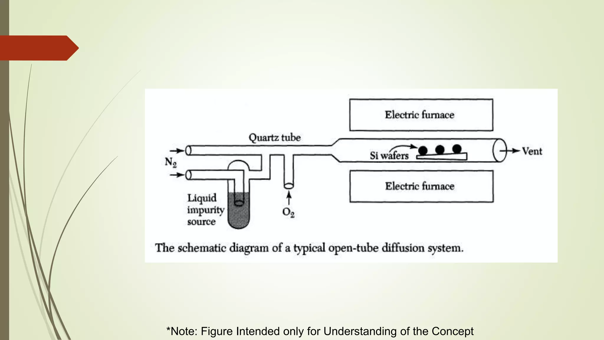
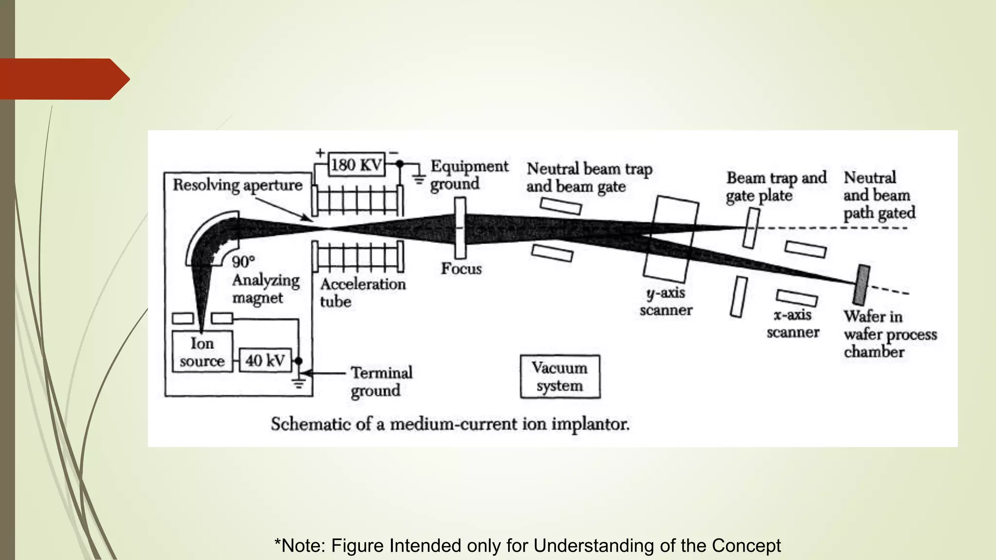


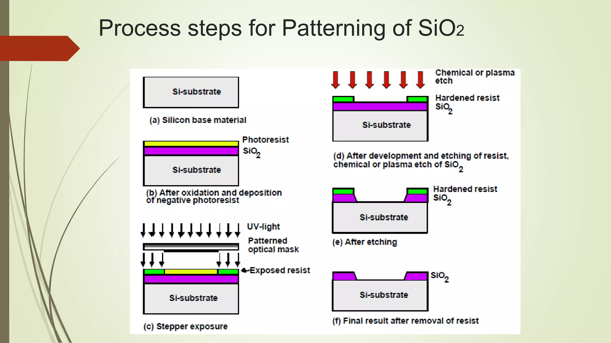


The document describes the key steps in the fabrication process of integrated circuits, including crystal growth, epitaxial growth, oxidation, doping, deposition, lithography, and etching. Crystal growth involves slowly withdrawing a silicon seed crystal from a melt of polycrystalline silicon to form a single crystal ingot. Epitaxial growth uses chemical vapor deposition or molecular beam epitaxy to form single-crystal layers on a substrate. Oxidation grows silicon dioxide layers via thermal oxidation. Doping introduces impurities via diffusion or ion implantation to modify conductivity. Lithography transfers circuit patterns to photoresist using a mask and photochemical processes.