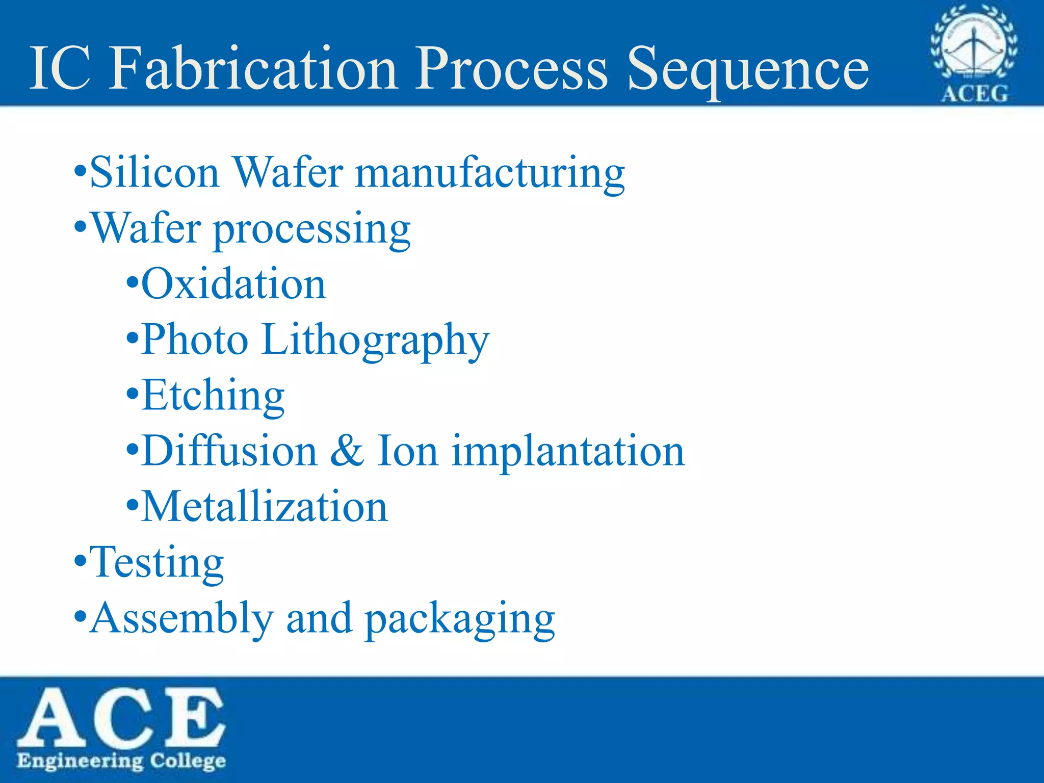
The IC fabrication process involves numerous steps:
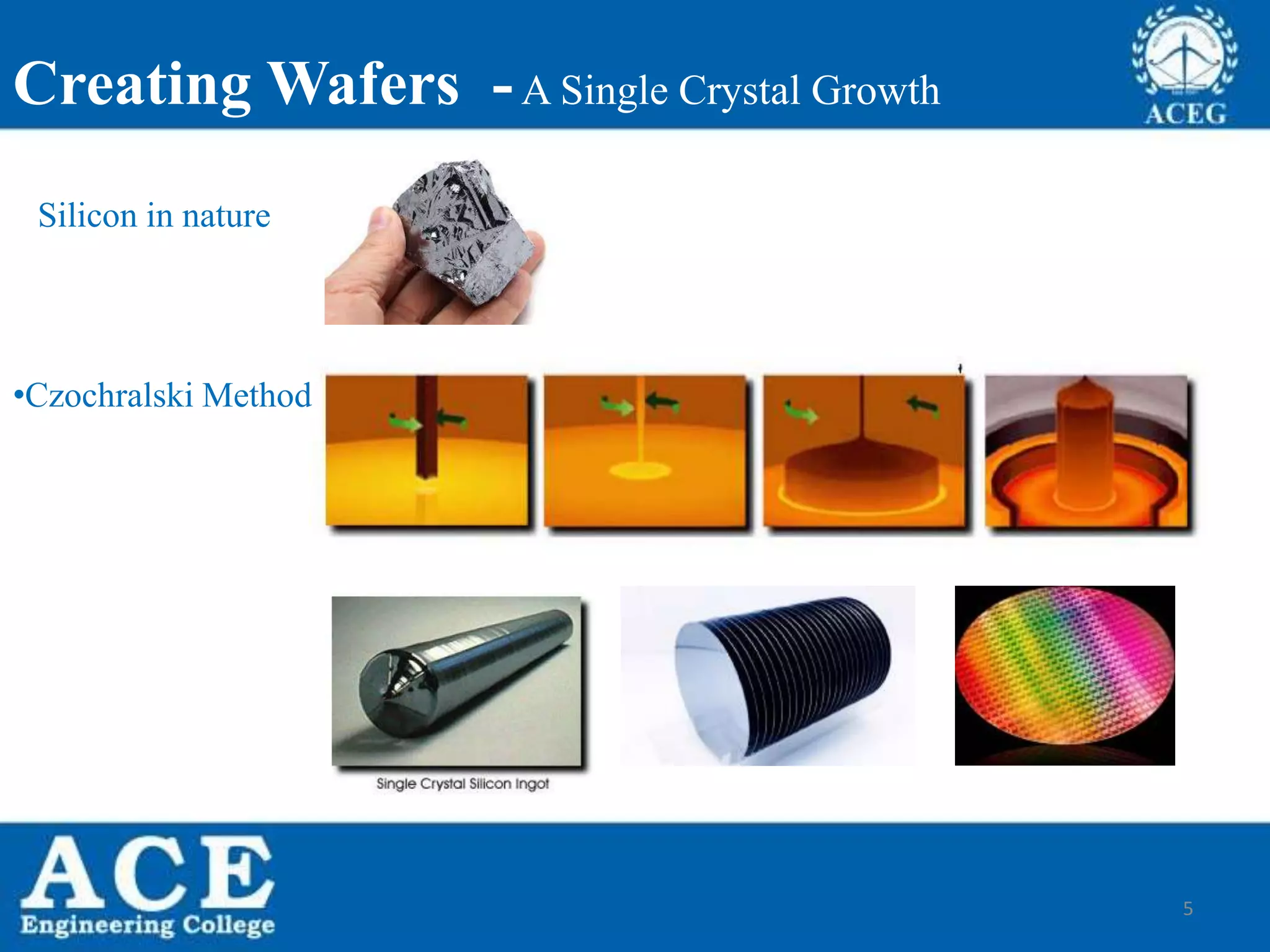
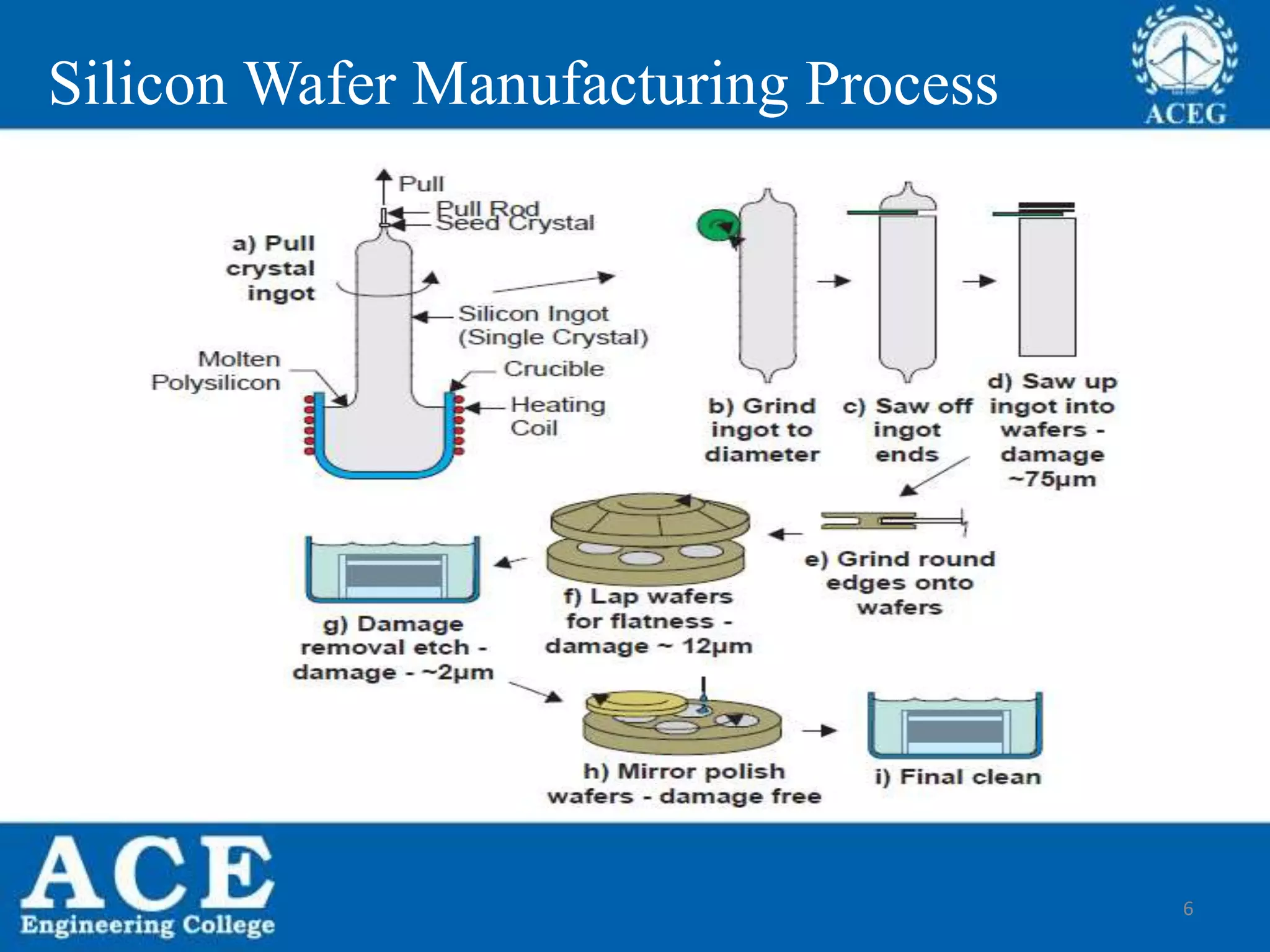
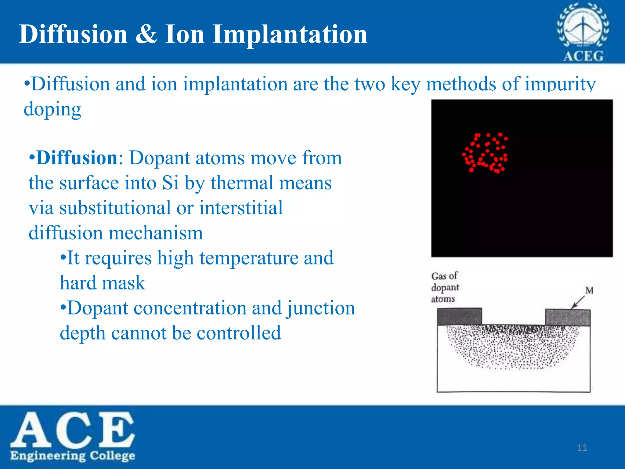
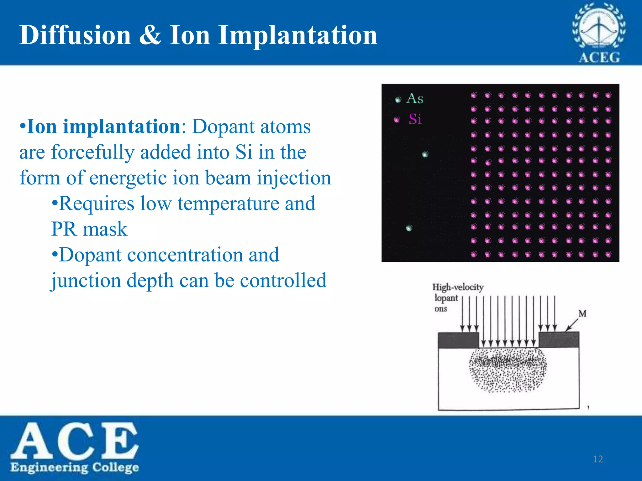
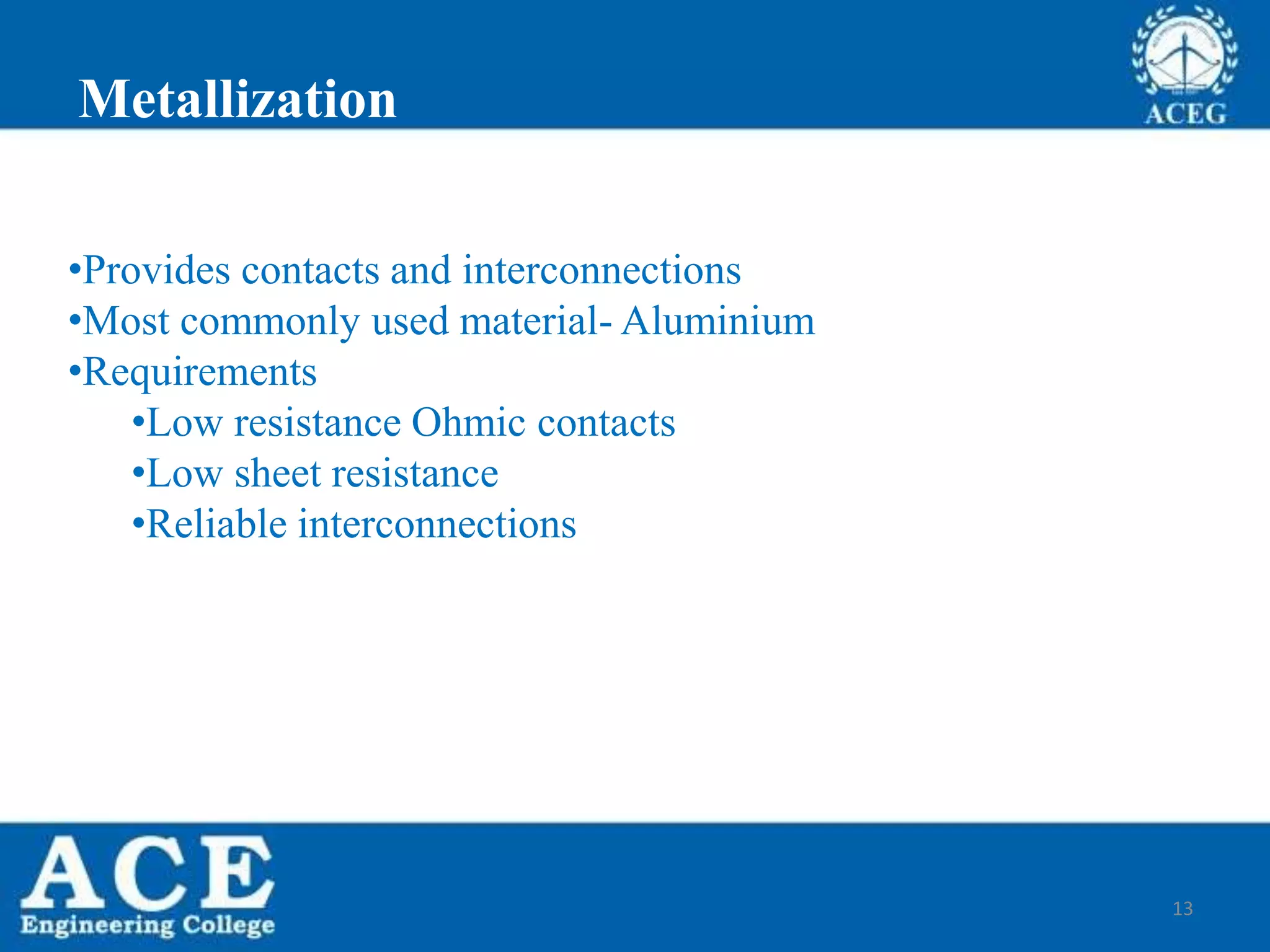
1) Silicon wafers are manufactured through processes like Czochralski crystal growth and then undergo oxidation, photolithography, etching, diffusion/ion implantation, and metallization.
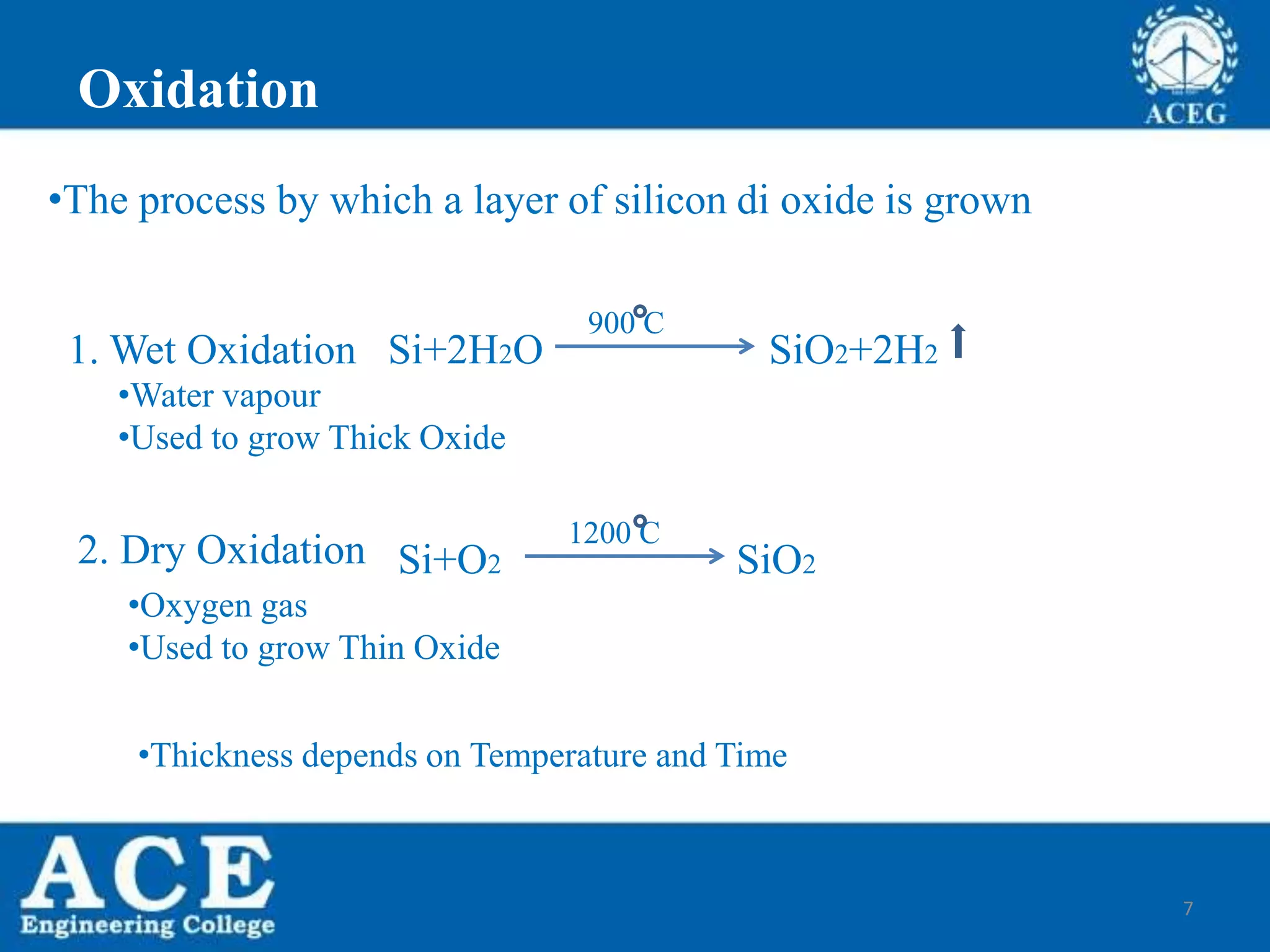
2) Oxidation grows insulating silicon dioxide layers on the wafer through wet or dry processes.
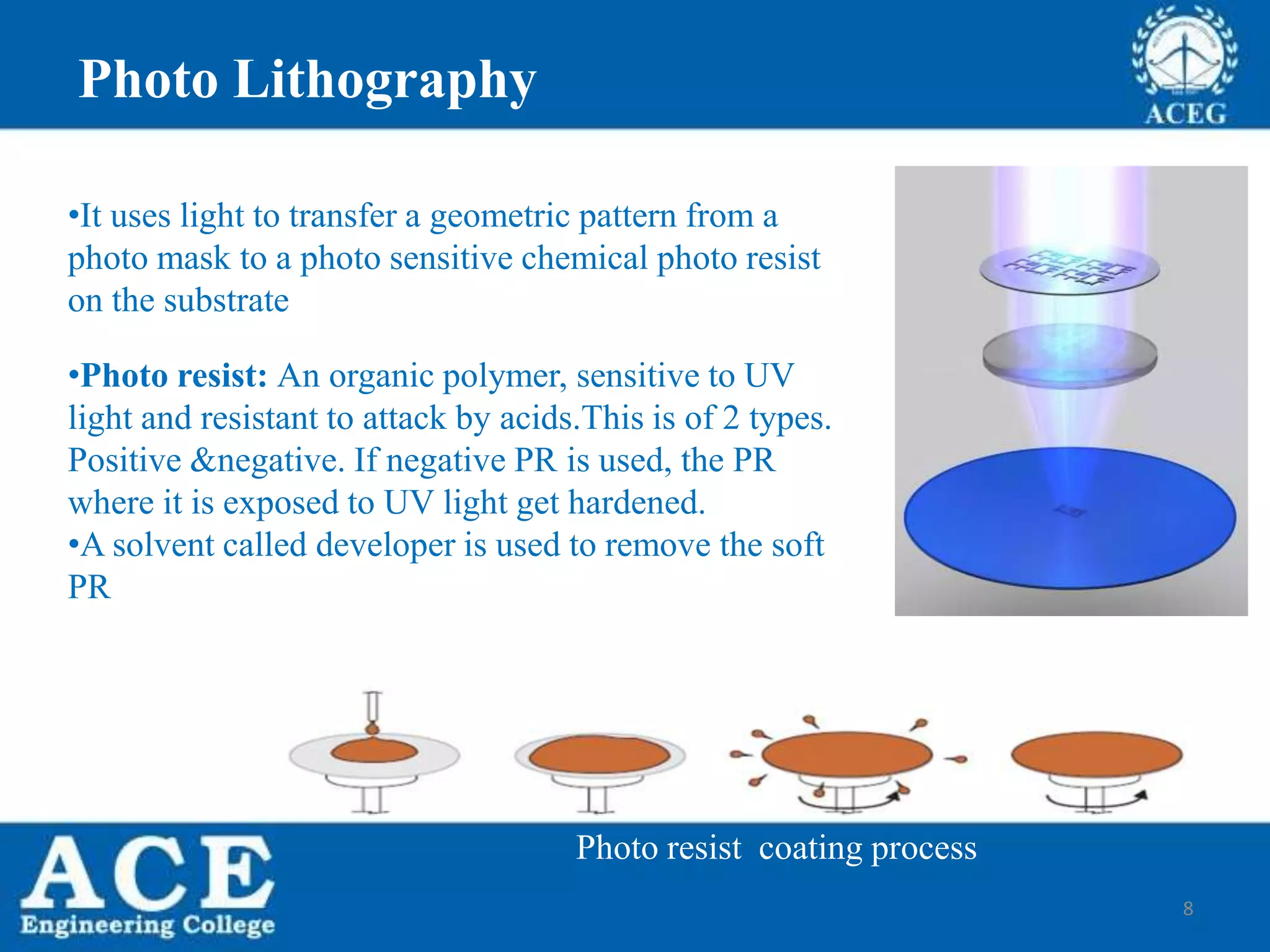
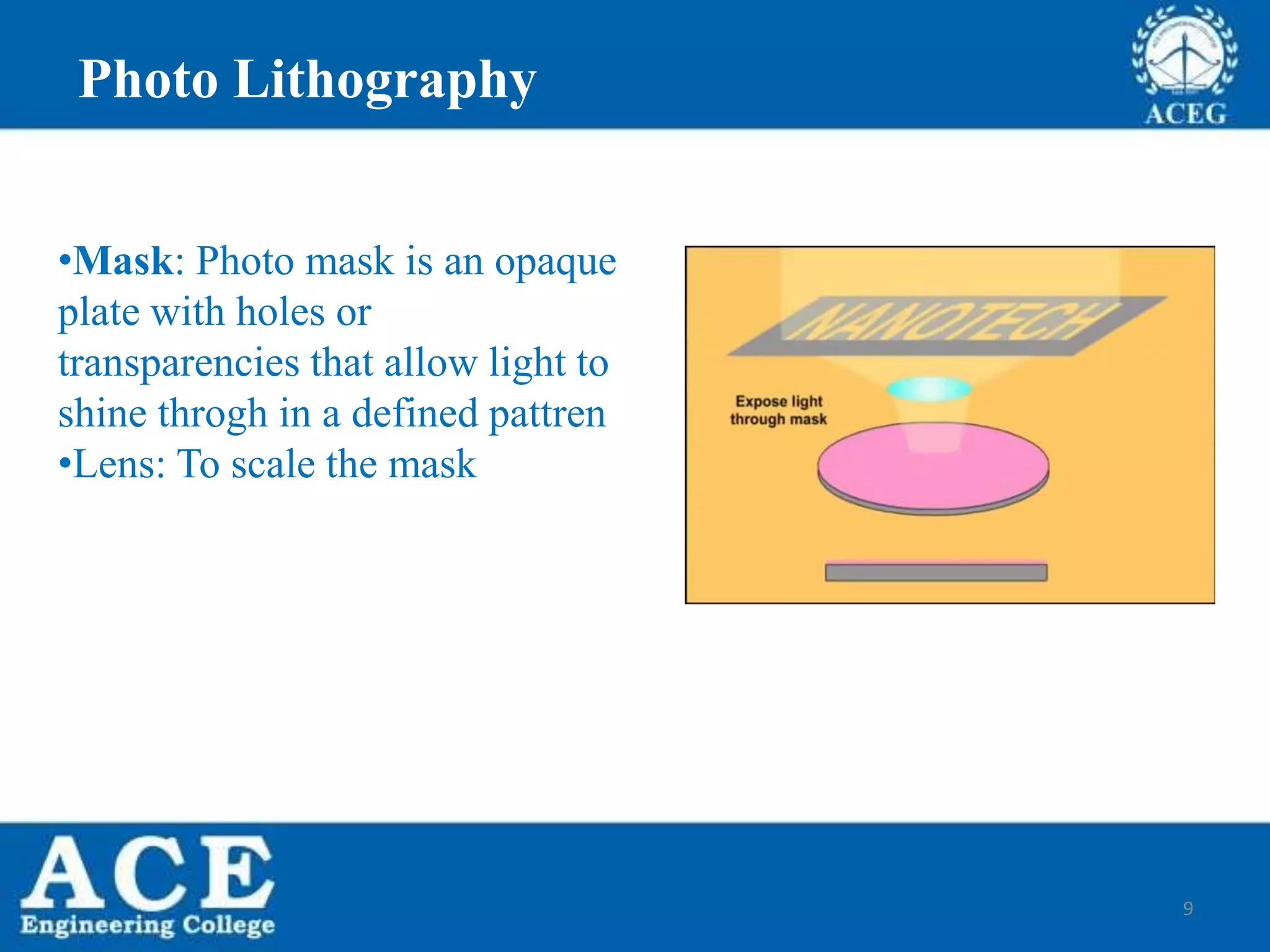
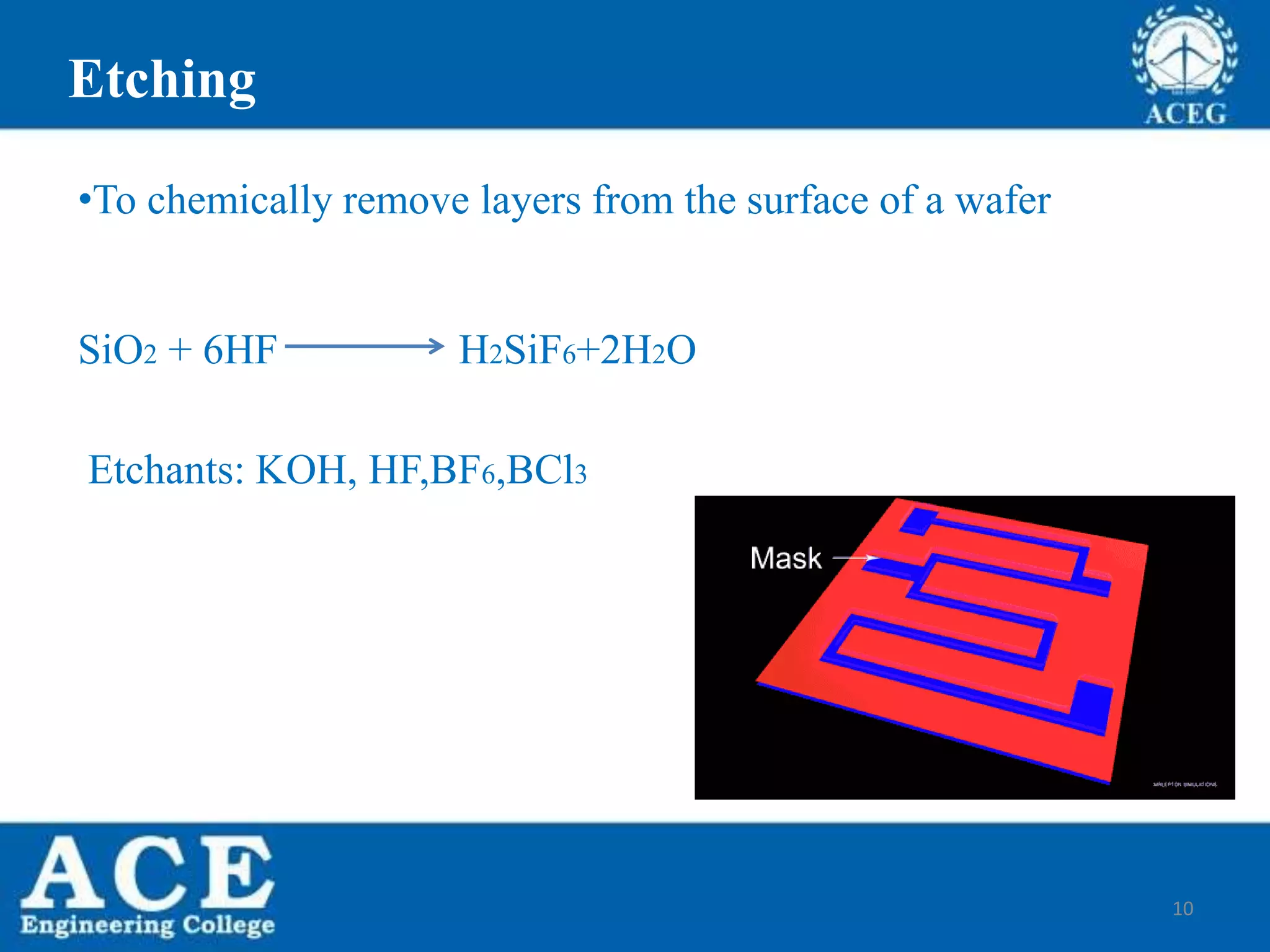
3) Photolithography uses a mask and light to transfer circuit patterns to photoresist before etching removes exposed material.