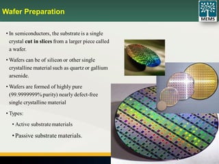
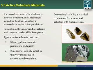
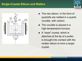
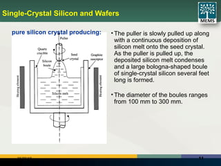
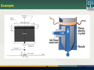
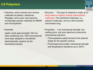
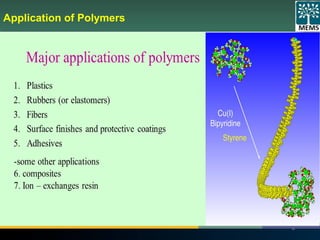
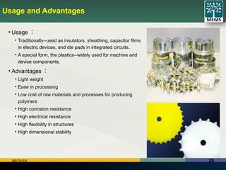
SlideShare a Scribd company logo
Chapter 3
Materials for MEMS & Microsystems
1
Outline
3.1 Introduction
3.2 Substrates and Wafers
3.3 Active Substrate Materials
3.4 Silicon as a Substrate Material
3.5 Silicon Compounds
3.6 Quartz
3.7 Piezoelectric Crystals
3.8 Polymers
3.9 Packaging Materials
3.10 Fabrication of Pressure Sensor.
2
3.1 Introduction
• The current technologies used in producing MEMS and microsystems are inseparable from
those of microelectronics.
• Many microsystems use microelectronics materials such as silicon, and gallium arsenide
(GaAs) for the sensing or actuating elements.
• These materials are chosen mainly because they are dimensionally stable and their
microfabrication and packaging techniques are well established in microelectronics.
• Other materials used for MEMS and microsystems products:
• quartz and Pyrex, polymers and plastics, and ceramics―that are not commonly used in
microelectronics.
• Plastics and polymers — used extensively in the case of microsystems produced by the
LIGA processes.
3
3.2 Substrates and Wafers
• Substrate:
• Micro fabricated devices are not generally freestanding (separate) devices but
are usually formed over or in a thicker support substrate.
• For electronic applications, semiconducting substrates such as silicon wafers
can be used. For optical devices or flat panel displays, transparent substrates
such as glass or quartz are common.
• The substrate enables easy handling of the micro device through the many
fabrication steps. Often many individual devices are made together on one
substrate and then singulated into separated devices toward the end of
fabrication.
Examples:
• Pressure sensors that convert the applied pressure to the deflection of a thin
diaphragm that is an integral part of a silicon die cut from a silicon substrate.
4
Wafer Preparation
5
6
Wafer Preparation
3.3 Active Substrate Materials
7
3.4 Silicon as a Substrate Material
• The Ideal Substrate for MEMS
• Single-Crystal Silicon and Wafers
• Crystal Structure
• Mechanical Properties of Silicon
8
The Ideal Substrate for MEMS
• It is mechanically stable and it can be integrated into electronics on the same substrate.
• Silicon is almost an ideal structural material. It has about the same Young’s modulus as steel
(about 2 × 10⁵
MPa), but is as light as aluminum.
• It has a melting point at 1400 , which is about twice as high as that of aluminum. This high℃
melting point makes silicon dimensionally stable even at elevated temperature.
• Its thermal expansion coefficient is about 8 times smaller than that of steel, and is more than
10 times smaller than that of aluminum.
9
10
Single-Crystal Silicon and Wafers
1106/25/18
Single-Crystal Silicon and Wafers
• The puller is slowly pulled up along
with a continuous deposition of
silicon melt onto the seed crystal.
As the puller is pulled up, the
deposited silicon melt condenses
and a large bologna-shaped boule
of single-crystal silicon several feet
long is formed.
• The diameter of the boules ranges
from 100 mm to 300 mm.
pure silicon crystal producing:
single-crystal silicon boule
12
Silicon wafer producing
13
Silicon wafer producing
14
Crystal Structure
15
 Silicon has basically a FCC unit
cell.
 In a typical FCC (face centered
cubic) crystal, atoms are situated at
the eight corners of the cubic lattice
structure, as well as at the center of
each of the six faces.
3.4.5 Mechanical Properties of Silicon
16
• Silicon is an elastic material with no plasticity or creep below 800 .℃
• It shows virtually no fatigue under all conceivable circumstance. These unique
characteristics make it an ideal material for sensing and actuating in microsystems.
• However, it is a brittle material. Therefore, undesirable brittle fracture behavior with
weak resistance to impact loads needs to be considered in the design of such
microsystems.
• Another disadvantage of silicon substrates is that they are anisotropic. This makes
accurate stress analysis of silicon structures tedious, since directional mechanical
property must be included.
3.5 Silicon Compounds
17
 3.5.1 Silicon Dioxide
 3.5.2 Silicon Carbide
 3.5.3 Silicon Nitride
 3.5.4 Polycrystalline Silicon
1806/25/18
3.5.1 Silicon Dioxide
• Principal uses:
• as a thermal and electric insulator,
• as a mask in the etching of silicon substrates,
• as a sacrificial layer in surface micromachining.
• Has much stronger resistance to most etchants
than silicon.
• Production:
• heating silicon in an oxidant such as oxygen
with or without steam. Chemical reactions for
such processes
• “dry” oxidation Si + O2 → SiO2
• “wet” oxidation Si + 2H2O → SiO2 + 2H2
1906/25/18
3.5.2 Silicon carbide
• Principal applications:
• Its dimensional and chemical stability at high temperatures.
• very strong resistance to oxidation even at very high temperatures.
• Thin films of silicon carbide are often deposited over MEMS components to
protect them from extreme temperature.
2006/25/18
3.6 Quartz
• Composition : Quartz is a compound of SiO2.
• Characteristics and application :
• an ideal material for sensors because of its near
absolute thermal dimensional stability.
• used in many piezoelectric devices.
• wristwatches, electronic filters, resonators.
• Inexpensive.
• Transparent to ultraviolet light, which is often used
to detect the various species in the fluid.
• Machine :
• diamond cutting
• ultrasonic cutting
http://baike.so.com/doc/5402201.html
2106/25/18
3.7 Piezoelectric Crystals
• Piezoelectric crystals are the solids of ceramic compounds that can
produce a voltage when a mechanical force is applied between
their faces.
• The reverse situation, that is the application of voltage to the crystal,
can also change its shape.
• This unique material behavior is called the piezoelectric effect.
22 06/25/18
Example
23 06/25/18
3.8 Polymers
• Polymers, which include such diverse
materials as plastics, adhesives,
Plexiglas, and Lucite, have become
increasingly popular materials for MEMS
and microsystems.
• Example:
plastic cards approximately 150 mm
wide containing over 1000 microchannel
have been adopted in microfluidic
electrophoretic systems by the
biomedical industry.
• Structure : This type of material is made up of
long chains of organic (mainly hydrocarbon)
molecules. The combined molecules, i.e.,
polymer molecules, can be a few hundred
nanometers long.
• Properties : Low mechanical strength, low
melting point, and poor electrical conductivity
characterize polymers.
• Thermoplastics-easily formed to the desired
shape for the specific product
• Thermosets-have better mechanical strength
and temperature resistance up to 350 .℃
Application of Polymers
24
2506/25/18
Usage and Advantages
• Usage :
• Traditionally--used as insulators, sheathing, capacitor films
in electric devices, and die pads in integrated circuits.
• A special form, the plastics--widely used for machine and
device components.
• Advantages :
• Light weight
• Ease in processing
• Low cost of raw materials and processes for producing
polymers
• High corrosion resistance
• High electrical resistance
• High flexibility in structures
• High dimensional stability
Polymers for MEMS and Microsystems
26
• Photoresist polymers are used to produce masks for creating desired patterns on
substrates by photolithography.
• The same photoresist polymers are used to produce the prime mold with the desired
geometry of MEMS components in the LIGA process for manufacturing micro device
components.
• These prime molds are plated with metals such as nickel for subsequent injection molding
for mass production of microcomponents.
27 06/25/18
Conductive Polymers
• For polymers to be used in certain applications in
microelectronics, MEMS, and microsystems, they
have to be made electrically conductive with
superior dimensional stability.
• Polymers have been used extensively in the
packaging of MEMS, but they have also been used
as substrates for some MEMS components in recent
years with the successful development of
techniques for controlling the electric conductivity
of these materials.
• Pyrolysis:
• A pyro polymer can be made electrically
conductive by adding an amine heated
above 600 .℃
• conductivity-- 2.7 ×10⁴
S/m>carbon.
• Doping
• Insertion of Conductive Fibers
3.9 Packaging Materials
28
• Differences:
• IC—protect the IC die and the interconnects from the often hostile operating
environment.
• microsystem—not only are the sensing or actuating elements to be protected, but they are
also required to be in contact with the media that are the sources of actions. Many of
these media are hostile to these elements.
• Materials: wires made of noble metals, metal layers for lead wires, solders for die/constraint
base attachments, etc., metals and plastics
IC Packaging Process:
29
3006/25/18
3.9 Packaging Materials
• Applications:
• aluminum or gold metal films—ohmic
contacts, lead wires
• plastic or stainless steel—casing
• Glass—constraint bases.
• tin-lead solder alloys or epoxy resins or RTV
—adhesive
• Copper and aluminum—metal
layers(sputtered)
• silicone gel or silicone oil—shield silicon
diaphragm etc.
3.10 Fabrication of Pressure Sensor :
31

More Related Content

What's hot

MEMS Packaging
MEMS PackagingMEMS Packaging
MEMS Packaging
Prasanna3804
 
Mems sensor
Mems sensorMems sensor
Mems sensor
FAIZAN AHMAD
 
MEMS an overview and application
MEMS an overview and applicationMEMS an overview and application
MEMS an overview and application
minajoddin
 
Micro Electro-mechanical system
Micro Electro-mechanical systemMicro Electro-mechanical system
Micro Electro-mechanical system
Mohit Singh Rajput
 
Mems (Detail Presentation)
Mems (Detail Presentation)Mems (Detail Presentation)
Mems (Detail Presentation)
Vinayak Hegde
 
Micro electro mechanical systems
Micro electro mechanical systemsMicro electro mechanical systems
Micro electro mechanical systems
sree navya
 
Mems presentation
Mems presentationMems presentation
Mems presentation
Michael Joshua S
 
Mems technologies and analysis of merits and demerits
Mems technologies and analysis of merits and demeritsMems technologies and analysis of merits and demerits
Mems technologies and analysis of merits and demerits
Biprasish Ray
 
Mems technology
Mems technologyMems technology
Mems technology
Dhaval Kaneria
 
LIGA Process
LIGA ProcessLIGA Process
LIGA Process
aman1312
 
Mems technology
Mems technologyMems technology
Mems technology
amit parcha
 
MEMS Techanology full seminar report
MEMS Techanology full seminar  reportMEMS Techanology full seminar  report
MEMS Techanology full seminar report
gautam221094
 
An introduction to mems technology
An introduction to mems technologyAn introduction to mems technology
An introduction to mems technology
sathish shankar
 
INTRODUCTION - MEMS
INTRODUCTION - MEMSINTRODUCTION - MEMS
INTRODUCTION - MEMS
Mohd Azrin Razali
 
Mems in medical technology
Mems in medical technologyMems in medical technology
Mems in medical technology
Satyanarayana Tammana
 
Micro electro-mechanical-systems-based-sensors
Micro electro-mechanical-systems-based-sensorsMicro electro-mechanical-systems-based-sensors
Micro electro-mechanical-systems-based-sensors
Muhammad Ali Amjad
 
Photolithography
PhotolithographyPhotolithography
Photolithography
tabirsir
 
Micro Electro Mechanical systems
Micro Electro Mechanical systemsMicro Electro Mechanical systems
Micro Electro Mechanical systemsVinodh Yadav
 

What's hot (20)

MEMS Packaging
MEMS PackagingMEMS Packaging
MEMS Packaging
 
Mems sensor
Mems sensorMems sensor
Mems sensor
 
MEMS an overview and application
MEMS an overview and applicationMEMS an overview and application
MEMS an overview and application
 
Micro Electro-mechanical system
Micro Electro-mechanical systemMicro Electro-mechanical system
Micro Electro-mechanical system
 
Nems2
Nems2Nems2
Nems2
 
mems ppt
mems pptmems ppt
mems ppt
 
Mems (Detail Presentation)
Mems (Detail Presentation)Mems (Detail Presentation)
Mems (Detail Presentation)
 
Micro electro mechanical systems
Micro electro mechanical systemsMicro electro mechanical systems
Micro electro mechanical systems
 
Mems presentation
Mems presentationMems presentation
Mems presentation
 
Mems technologies and analysis of merits and demerits
Mems technologies and analysis of merits and demeritsMems technologies and analysis of merits and demerits
Mems technologies and analysis of merits and demerits
 
Mems technology
Mems technologyMems technology
Mems technology
 
LIGA Process
LIGA ProcessLIGA Process
LIGA Process
 
Mems technology
Mems technologyMems technology
Mems technology
 
MEMS Techanology full seminar report
MEMS Techanology full seminar  reportMEMS Techanology full seminar  report
MEMS Techanology full seminar report
 
An introduction to mems technology
An introduction to mems technologyAn introduction to mems technology
An introduction to mems technology
 
INTRODUCTION - MEMS
INTRODUCTION - MEMSINTRODUCTION - MEMS
INTRODUCTION - MEMS
 
Mems in medical technology
Mems in medical technologyMems in medical technology
Mems in medical technology
 
Micro electro-mechanical-systems-based-sensors
Micro electro-mechanical-systems-based-sensorsMicro electro-mechanical-systems-based-sensors
Micro electro-mechanical-systems-based-sensors
 
Photolithography
PhotolithographyPhotolithography
Photolithography
 
Micro Electro Mechanical systems
Micro Electro Mechanical systemsMicro Electro Mechanical systems
Micro Electro Mechanical systems
 

Similar to Materials for MEMS

Materials for MEMS.pdf
Materials for MEMS.pdfMaterials for MEMS.pdf
Materials for MEMS.pdf
SreejaSujith2
 
9MEMSU3.pdf
9MEMSU3.pdf9MEMSU3.pdf
9MEMSU3.pdf
harikamivaan
 
The radio frequency microelectromechanical system (RF MEMS) Materials
The radio frequency microelectromechanical system (RF MEMS)  Materials The radio frequency microelectromechanical system (RF MEMS)  Materials
The radio frequency microelectromechanical system (RF MEMS) Materials
Jitendra Jangid
 
Mems (micro electro mechanical systems)
Mems (micro electro mechanical systems)Mems (micro electro mechanical systems)
Mems (micro electro mechanical systems)
JDReddy
 
Metallic Micro Lattice
Metallic Micro LatticeMetallic Micro Lattice
Mems manufacturing
Mems manufacturingMems manufacturing
Mems manufacturing
Shubham Gupta
 
Mems unit 1-lec_1
Mems unit 1-lec_1Mems unit 1-lec_1
Mems unit 1-lec_1
BRAHMANAND SINGH
 
Smart material
Smart materialSmart material
Smart material
prashant singh
 
9MEMSU1.pdf
9MEMSU1.pdf9MEMSU1.pdf
9MEMSU1.pdf
harikamivaan
 
BME PE501 BIO MEMS K.BASHKARAN.pptx
BME PE501 BIO MEMS K.BASHKARAN.pptxBME PE501 BIO MEMS K.BASHKARAN.pptx
BME PE501 BIO MEMS K.BASHKARAN.pptx
BashkaranK
 
A review about various types of solar panels
A review about various types of solar panelsA review about various types of solar panels
A review about various types of solar panels
RanjuRajan3
 
Metallic glasses
Metallic glassesMetallic glasses
Metallic glasses
Moxit Khandhar
 
Micro-electro-mechanical Systems
Micro-electro-mechanical Systems Micro-electro-mechanical Systems
Micro-electro-mechanical Systems
utpal sarkar
 
Chapter 1 Introduction to Materials Science and Engineering
Chapter 1 Introduction to Materials Science and Engineering Chapter 1 Introduction to Materials Science and Engineering
Chapter 1 Introduction to Materials Science and Engineering
Pem(ເປ່ມ) PHAKVISETH
 
APPLICATION OF FIBRE IN NUCLEAR ENERGY PLANT
APPLICATION OF FIBRE IN NUCLEAR ENERGY PLANTAPPLICATION OF FIBRE IN NUCLEAR ENERGY PLANT
APPLICATION OF FIBRE IN NUCLEAR ENERGY PLANT
Amal Ray
 
Advanced ceramics
Advanced ceramicsAdvanced ceramics
Introduction about semiconductors and their integration with nanomaterial
Introduction about semiconductors and their integration with nanomaterialIntroduction about semiconductors and their integration with nanomaterial
Introduction about semiconductors and their integration with nanomaterial
Abhay Rajput
 
VLSI Technology.pptx
VLSI Technology.pptxVLSI Technology.pptx
VLSI Technology.pptx
kiran27822
 
Solar cell.pptx
Solar cell.pptxSolar cell.pptx
Solar cell.pptx
abcd463546
 

Similar to Materials for MEMS (20)

Materials for MEMS.pdf
Materials for MEMS.pdfMaterials for MEMS.pdf
Materials for MEMS.pdf
 
9MEMSU3.pdf
9MEMSU3.pdf9MEMSU3.pdf
9MEMSU3.pdf
 
The radio frequency microelectromechanical system (RF MEMS) Materials
The radio frequency microelectromechanical system (RF MEMS)  Materials The radio frequency microelectromechanical system (RF MEMS)  Materials
The radio frequency microelectromechanical system (RF MEMS) Materials
 
Mems (micro electro mechanical systems)
Mems (micro electro mechanical systems)Mems (micro electro mechanical systems)
Mems (micro electro mechanical systems)
 
Metallic Micro Lattice
Metallic Micro LatticeMetallic Micro Lattice
Metallic Micro Lattice
 
Mems manufacturing
Mems manufacturingMems manufacturing
Mems manufacturing
 
Mems brahma
Mems brahmaMems brahma
Mems brahma
 
Mems unit 1-lec_1
Mems unit 1-lec_1Mems unit 1-lec_1
Mems unit 1-lec_1
 
Smart material
Smart materialSmart material
Smart material
 
9MEMSU1.pdf
9MEMSU1.pdf9MEMSU1.pdf
9MEMSU1.pdf
 
BME PE501 BIO MEMS K.BASHKARAN.pptx
BME PE501 BIO MEMS K.BASHKARAN.pptxBME PE501 BIO MEMS K.BASHKARAN.pptx
BME PE501 BIO MEMS K.BASHKARAN.pptx
 
A review about various types of solar panels
A review about various types of solar panelsA review about various types of solar panels
A review about various types of solar panels
 
Metallic glasses
Metallic glassesMetallic glasses
Metallic glasses
 
Micro-electro-mechanical Systems
Micro-electro-mechanical Systems Micro-electro-mechanical Systems
Micro-electro-mechanical Systems
 
Chapter 1 Introduction to Materials Science and Engineering
Chapter 1 Introduction to Materials Science and Engineering Chapter 1 Introduction to Materials Science and Engineering
Chapter 1 Introduction to Materials Science and Engineering
 
APPLICATION OF FIBRE IN NUCLEAR ENERGY PLANT
APPLICATION OF FIBRE IN NUCLEAR ENERGY PLANTAPPLICATION OF FIBRE IN NUCLEAR ENERGY PLANT
APPLICATION OF FIBRE IN NUCLEAR ENERGY PLANT
 
Advanced ceramics
Advanced ceramicsAdvanced ceramics
Advanced ceramics
 
Introduction about semiconductors and their integration with nanomaterial
Introduction about semiconductors and their integration with nanomaterialIntroduction about semiconductors and their integration with nanomaterial
Introduction about semiconductors and their integration with nanomaterial
 
VLSI Technology.pptx
VLSI Technology.pptxVLSI Technology.pptx
VLSI Technology.pptx
 
Solar cell.pptx
Solar cell.pptxSolar cell.pptx
Solar cell.pptx
 

Recently uploaded

Top 10 Oil and Gas Projects in Saudi Arabia 2024.pdf
Top 10 Oil and Gas Projects in Saudi Arabia 2024.pdfTop 10 Oil and Gas Projects in Saudi Arabia 2024.pdf
Top 10 Oil and Gas Projects in Saudi Arabia 2024.pdf
Teleport Manpower Consultant
 
The Benefits and Techniques of Trenchless Pipe Repair.pdf
The Benefits and Techniques of Trenchless Pipe Repair.pdfThe Benefits and Techniques of Trenchless Pipe Repair.pdf
The Benefits and Techniques of Trenchless Pipe Repair.pdf
Pipe Restoration Solutions
 
LIGA(E)11111111111111111111111111111111111111111.ppt
LIGA(E)11111111111111111111111111111111111111111.pptLIGA(E)11111111111111111111111111111111111111111.ppt
LIGA(E)11111111111111111111111111111111111111111.ppt
ssuser9bd3ba
 
在线办理(ANU毕业证书)澳洲国立大学毕业证录取通知书一模一样
在线办理(ANU毕业证书)澳洲国立大学毕业证录取通知书一模一样在线办理(ANU毕业证书)澳洲国立大学毕业证录取通知书一模一样
在线办理(ANU毕业证书)澳洲国立大学毕业证录取通知书一模一样
obonagu
 
Vaccine management system project report documentation..pdf
Vaccine management system project report documentation..pdfVaccine management system project report documentation..pdf
Vaccine management system project report documentation..pdf
Kamal Acharya
 
COLLEGE BUS MANAGEMENT SYSTEM PROJECT REPORT.pdf
COLLEGE BUS MANAGEMENT SYSTEM PROJECT REPORT.pdfCOLLEGE BUS MANAGEMENT SYSTEM PROJECT REPORT.pdf
COLLEGE BUS MANAGEMENT SYSTEM PROJECT REPORT.pdf
Kamal Acharya
 
CME397 Surface Engineering- Professional Elective
CME397 Surface Engineering- Professional ElectiveCME397 Surface Engineering- Professional Elective
CME397 Surface Engineering- Professional Elective
karthi keyan
 
Planning Of Procurement o different goods and services
Planning Of Procurement o different goods and servicesPlanning Of Procurement o different goods and services
Planning Of Procurement o different goods and services
JoytuBarua2
 
Nuclear Power Economics and Structuring 2024
Nuclear Power Economics and Structuring 2024Nuclear Power Economics and Structuring 2024
Nuclear Power Economics and Structuring 2024
Massimo Talia
 
Halogenation process of chemical process industries
Halogenation process of chemical process industriesHalogenation process of chemical process industries
Halogenation process of chemical process industries
MuhammadTufail242431
 
addressing modes in computer architecture
addressing modes  in computer architectureaddressing modes  in computer architecture
addressing modes in computer architecture
ShahidSultan24
 
Design and Analysis of Algorithms-DP,Backtracking,Graphs,B&B
Design and Analysis of Algorithms-DP,Backtracking,Graphs,B&BDesign and Analysis of Algorithms-DP,Backtracking,Graphs,B&B
Design and Analysis of Algorithms-DP,Backtracking,Graphs,B&B
Sreedhar Chowdam
 
J.Yang, ICLR 2024, MLILAB, KAIST AI.pdf
J.Yang,  ICLR 2024, MLILAB, KAIST AI.pdfJ.Yang,  ICLR 2024, MLILAB, KAIST AI.pdf
J.Yang, ICLR 2024, MLILAB, KAIST AI.pdf
MLILAB
 
CFD Simulation of By-pass Flow in a HRSG module by R&R Consult.pptx
CFD Simulation of By-pass Flow in a HRSG module by R&R Consult.pptxCFD Simulation of By-pass Flow in a HRSG module by R&R Consult.pptx
CFD Simulation of By-pass Flow in a HRSG module by R&R Consult.pptx
R&R Consult
 
Hybrid optimization of pumped hydro system and solar- Engr. Abdul-Azeez.pdf
Hybrid optimization of pumped hydro system and solar- Engr. Abdul-Azeez.pdfHybrid optimization of pumped hydro system and solar- Engr. Abdul-Azeez.pdf
Hybrid optimization of pumped hydro system and solar- Engr. Abdul-Azeez.pdf
fxintegritypublishin
 
一比一原版(SFU毕业证)西蒙菲莎大学毕业证成绩单如何办理
一比一原版(SFU毕业证)西蒙菲莎大学毕业证成绩单如何办理一比一原版(SFU毕业证)西蒙菲莎大学毕业证成绩单如何办理
一比一原版(SFU毕业证)西蒙菲莎大学毕业证成绩单如何办理
bakpo1
 
MCQ Soil mechanics questions (Soil shear strength).pdf
MCQ Soil mechanics questions (Soil shear strength).pdfMCQ Soil mechanics questions (Soil shear strength).pdf
MCQ Soil mechanics questions (Soil shear strength).pdf
Osamah Alsalih
 
Forklift Classes Overview by Intella Parts
Forklift Classes Overview by Intella PartsForklift Classes Overview by Intella Parts
Forklift Classes Overview by Intella Parts
Intella Parts
 
Quality defects in TMT Bars, Possible causes and Potential Solutions.
Quality defects in TMT Bars, Possible causes and Potential Solutions.Quality defects in TMT Bars, Possible causes and Potential Solutions.
Quality defects in TMT Bars, Possible causes and Potential Solutions.
PrashantGoswami42
 
weather web application report.pdf
weather web application report.pdfweather web application report.pdf
weather web application report.pdf
Pratik Pawar
 

Recently uploaded (20)

Top 10 Oil and Gas Projects in Saudi Arabia 2024.pdf
Top 10 Oil and Gas Projects in Saudi Arabia 2024.pdfTop 10 Oil and Gas Projects in Saudi Arabia 2024.pdf
Top 10 Oil and Gas Projects in Saudi Arabia 2024.pdf
 
The Benefits and Techniques of Trenchless Pipe Repair.pdf
The Benefits and Techniques of Trenchless Pipe Repair.pdfThe Benefits and Techniques of Trenchless Pipe Repair.pdf
The Benefits and Techniques of Trenchless Pipe Repair.pdf
 
LIGA(E)11111111111111111111111111111111111111111.ppt
LIGA(E)11111111111111111111111111111111111111111.pptLIGA(E)11111111111111111111111111111111111111111.ppt
LIGA(E)11111111111111111111111111111111111111111.ppt
 
在线办理(ANU毕业证书)澳洲国立大学毕业证录取通知书一模一样
在线办理(ANU毕业证书)澳洲国立大学毕业证录取通知书一模一样在线办理(ANU毕业证书)澳洲国立大学毕业证录取通知书一模一样
在线办理(ANU毕业证书)澳洲国立大学毕业证录取通知书一模一样
 
Vaccine management system project report documentation..pdf
Vaccine management system project report documentation..pdfVaccine management system project report documentation..pdf
Vaccine management system project report documentation..pdf
 
COLLEGE BUS MANAGEMENT SYSTEM PROJECT REPORT.pdf
COLLEGE BUS MANAGEMENT SYSTEM PROJECT REPORT.pdfCOLLEGE BUS MANAGEMENT SYSTEM PROJECT REPORT.pdf
COLLEGE BUS MANAGEMENT SYSTEM PROJECT REPORT.pdf
 
CME397 Surface Engineering- Professional Elective
CME397 Surface Engineering- Professional ElectiveCME397 Surface Engineering- Professional Elective
CME397 Surface Engineering- Professional Elective
 
Planning Of Procurement o different goods and services
Planning Of Procurement o different goods and servicesPlanning Of Procurement o different goods and services
Planning Of Procurement o different goods and services
 
Nuclear Power Economics and Structuring 2024
Nuclear Power Economics and Structuring 2024Nuclear Power Economics and Structuring 2024
Nuclear Power Economics and Structuring 2024
 
Halogenation process of chemical process industries
Halogenation process of chemical process industriesHalogenation process of chemical process industries
Halogenation process of chemical process industries
 
addressing modes in computer architecture
addressing modes  in computer architectureaddressing modes  in computer architecture
addressing modes in computer architecture
 
Design and Analysis of Algorithms-DP,Backtracking,Graphs,B&B
Design and Analysis of Algorithms-DP,Backtracking,Graphs,B&BDesign and Analysis of Algorithms-DP,Backtracking,Graphs,B&B
Design and Analysis of Algorithms-DP,Backtracking,Graphs,B&B
 
J.Yang, ICLR 2024, MLILAB, KAIST AI.pdf
J.Yang,  ICLR 2024, MLILAB, KAIST AI.pdfJ.Yang,  ICLR 2024, MLILAB, KAIST AI.pdf
J.Yang, ICLR 2024, MLILAB, KAIST AI.pdf
 
CFD Simulation of By-pass Flow in a HRSG module by R&R Consult.pptx
CFD Simulation of By-pass Flow in a HRSG module by R&R Consult.pptxCFD Simulation of By-pass Flow in a HRSG module by R&R Consult.pptx
CFD Simulation of By-pass Flow in a HRSG module by R&R Consult.pptx
 
Hybrid optimization of pumped hydro system and solar- Engr. Abdul-Azeez.pdf
Hybrid optimization of pumped hydro system and solar- Engr. Abdul-Azeez.pdfHybrid optimization of pumped hydro system and solar- Engr. Abdul-Azeez.pdf
Hybrid optimization of pumped hydro system and solar- Engr. Abdul-Azeez.pdf
 
一比一原版(SFU毕业证)西蒙菲莎大学毕业证成绩单如何办理
一比一原版(SFU毕业证)西蒙菲莎大学毕业证成绩单如何办理一比一原版(SFU毕业证)西蒙菲莎大学毕业证成绩单如何办理
一比一原版(SFU毕业证)西蒙菲莎大学毕业证成绩单如何办理
 
MCQ Soil mechanics questions (Soil shear strength).pdf
MCQ Soil mechanics questions (Soil shear strength).pdfMCQ Soil mechanics questions (Soil shear strength).pdf
MCQ Soil mechanics questions (Soil shear strength).pdf
 
Forklift Classes Overview by Intella Parts
Forklift Classes Overview by Intella PartsForklift Classes Overview by Intella Parts
Forklift Classes Overview by Intella Parts
 
Quality defects in TMT Bars, Possible causes and Potential Solutions.
Quality defects in TMT Bars, Possible causes and Potential Solutions.Quality defects in TMT Bars, Possible causes and Potential Solutions.
Quality defects in TMT Bars, Possible causes and Potential Solutions.
 
weather web application report.pdf
weather web application report.pdfweather web application report.pdf
weather web application report.pdf
 

Materials for MEMS

  • 1. Chapter 3 Materials for MEMS & Microsystems 1
  • 2. Outline 3.1 Introduction 3.2 Substrates and Wafers 3.3 Active Substrate Materials 3.4 Silicon as a Substrate Material 3.5 Silicon Compounds 3.6 Quartz 3.7 Piezoelectric Crystals 3.8 Polymers 3.9 Packaging Materials 3.10 Fabrication of Pressure Sensor. 2
  • 3. 3.1 Introduction • The current technologies used in producing MEMS and microsystems are inseparable from those of microelectronics. • Many microsystems use microelectronics materials such as silicon, and gallium arsenide (GaAs) for the sensing or actuating elements. • These materials are chosen mainly because they are dimensionally stable and their microfabrication and packaging techniques are well established in microelectronics. • Other materials used for MEMS and microsystems products: • quartz and Pyrex, polymers and plastics, and ceramics―that are not commonly used in microelectronics. • Plastics and polymers — used extensively in the case of microsystems produced by the LIGA processes. 3
  • 4. 3.2 Substrates and Wafers • Substrate: • Micro fabricated devices are not generally freestanding (separate) devices but are usually formed over or in a thicker support substrate. • For electronic applications, semiconducting substrates such as silicon wafers can be used. For optical devices or flat panel displays, transparent substrates such as glass or quartz are common. • The substrate enables easy handling of the micro device through the many fabrication steps. Often many individual devices are made together on one substrate and then singulated into separated devices toward the end of fabrication. Examples: • Pressure sensors that convert the applied pressure to the deflection of a thin diaphragm that is an integral part of a silicon die cut from a silicon substrate. 4
  • 7. 3.3 Active Substrate Materials 7
  • 8. 3.4 Silicon as a Substrate Material • The Ideal Substrate for MEMS • Single-Crystal Silicon and Wafers • Crystal Structure • Mechanical Properties of Silicon 8
  • 9. The Ideal Substrate for MEMS • It is mechanically stable and it can be integrated into electronics on the same substrate. • Silicon is almost an ideal structural material. It has about the same Young’s modulus as steel (about 2 × 10⁵ MPa), but is as light as aluminum. • It has a melting point at 1400 , which is about twice as high as that of aluminum. This high℃ melting point makes silicon dimensionally stable even at elevated temperature. • Its thermal expansion coefficient is about 8 times smaller than that of steel, and is more than 10 times smaller than that of aluminum. 9
  • 11. 1106/25/18 Single-Crystal Silicon and Wafers • The puller is slowly pulled up along with a continuous deposition of silicon melt onto the seed crystal. As the puller is pulled up, the deposited silicon melt condenses and a large bologna-shaped boule of single-crystal silicon several feet long is formed. • The diameter of the boules ranges from 100 mm to 300 mm. pure silicon crystal producing:
  • 15. Crystal Structure 15  Silicon has basically a FCC unit cell.  In a typical FCC (face centered cubic) crystal, atoms are situated at the eight corners of the cubic lattice structure, as well as at the center of each of the six faces.
  • 16. 3.4.5 Mechanical Properties of Silicon 16 • Silicon is an elastic material with no plasticity or creep below 800 .℃ • It shows virtually no fatigue under all conceivable circumstance. These unique characteristics make it an ideal material for sensing and actuating in microsystems. • However, it is a brittle material. Therefore, undesirable brittle fracture behavior with weak resistance to impact loads needs to be considered in the design of such microsystems. • Another disadvantage of silicon substrates is that they are anisotropic. This makes accurate stress analysis of silicon structures tedious, since directional mechanical property must be included.
  • 17. 3.5 Silicon Compounds 17  3.5.1 Silicon Dioxide  3.5.2 Silicon Carbide  3.5.3 Silicon Nitride  3.5.4 Polycrystalline Silicon
  • 18. 1806/25/18 3.5.1 Silicon Dioxide • Principal uses: • as a thermal and electric insulator, • as a mask in the etching of silicon substrates, • as a sacrificial layer in surface micromachining. • Has much stronger resistance to most etchants than silicon. • Production: • heating silicon in an oxidant such as oxygen with or without steam. Chemical reactions for such processes • “dry” oxidation Si + O2 → SiO2 • “wet” oxidation Si + 2H2O → SiO2 + 2H2
  • 19. 1906/25/18 3.5.2 Silicon carbide • Principal applications: • Its dimensional and chemical stability at high temperatures. • very strong resistance to oxidation even at very high temperatures. • Thin films of silicon carbide are often deposited over MEMS components to protect them from extreme temperature.
  • 20. 2006/25/18 3.6 Quartz • Composition : Quartz is a compound of SiO2. • Characteristics and application : • an ideal material for sensors because of its near absolute thermal dimensional stability. • used in many piezoelectric devices. • wristwatches, electronic filters, resonators. • Inexpensive. • Transparent to ultraviolet light, which is often used to detect the various species in the fluid. • Machine : • diamond cutting • ultrasonic cutting http://baike.so.com/doc/5402201.html
  • 21. 2106/25/18 3.7 Piezoelectric Crystals • Piezoelectric crystals are the solids of ceramic compounds that can produce a voltage when a mechanical force is applied between their faces. • The reverse situation, that is the application of voltage to the crystal, can also change its shape. • This unique material behavior is called the piezoelectric effect.
  • 23. 23 06/25/18 3.8 Polymers • Polymers, which include such diverse materials as plastics, adhesives, Plexiglas, and Lucite, have become increasingly popular materials for MEMS and microsystems. • Example: plastic cards approximately 150 mm wide containing over 1000 microchannel have been adopted in microfluidic electrophoretic systems by the biomedical industry. • Structure : This type of material is made up of long chains of organic (mainly hydrocarbon) molecules. The combined molecules, i.e., polymer molecules, can be a few hundred nanometers long. • Properties : Low mechanical strength, low melting point, and poor electrical conductivity characterize polymers. • Thermoplastics-easily formed to the desired shape for the specific product • Thermosets-have better mechanical strength and temperature resistance up to 350 .℃
  • 25. 2506/25/18 Usage and Advantages • Usage : • Traditionally--used as insulators, sheathing, capacitor films in electric devices, and die pads in integrated circuits. • A special form, the plastics--widely used for machine and device components. • Advantages : • Light weight • Ease in processing • Low cost of raw materials and processes for producing polymers • High corrosion resistance • High electrical resistance • High flexibility in structures • High dimensional stability
  • 26. Polymers for MEMS and Microsystems 26 • Photoresist polymers are used to produce masks for creating desired patterns on substrates by photolithography. • The same photoresist polymers are used to produce the prime mold with the desired geometry of MEMS components in the LIGA process for manufacturing micro device components. • These prime molds are plated with metals such as nickel for subsequent injection molding for mass production of microcomponents.
  • 27. 27 06/25/18 Conductive Polymers • For polymers to be used in certain applications in microelectronics, MEMS, and microsystems, they have to be made electrically conductive with superior dimensional stability. • Polymers have been used extensively in the packaging of MEMS, but they have also been used as substrates for some MEMS components in recent years with the successful development of techniques for controlling the electric conductivity of these materials. • Pyrolysis: • A pyro polymer can be made electrically conductive by adding an amine heated above 600 .℃ • conductivity-- 2.7 ×10⁴ S/m>carbon. • Doping • Insertion of Conductive Fibers
  • 28. 3.9 Packaging Materials 28 • Differences: • IC—protect the IC die and the interconnects from the often hostile operating environment. • microsystem—not only are the sensing or actuating elements to be protected, but they are also required to be in contact with the media that are the sources of actions. Many of these media are hostile to these elements. • Materials: wires made of noble metals, metal layers for lead wires, solders for die/constraint base attachments, etc., metals and plastics
  • 30. 3006/25/18 3.9 Packaging Materials • Applications: • aluminum or gold metal films—ohmic contacts, lead wires • plastic or stainless steel—casing • Glass—constraint bases. • tin-lead solder alloys or epoxy resins or RTV —adhesive • Copper and aluminum—metal layers(sputtered) • silicone gel or silicone oil—shield silicon diaphragm etc.
  • 31. 3.10 Fabrication of Pressure Sensor : 31