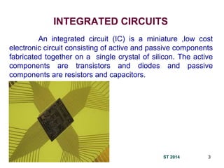
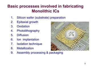
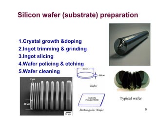
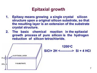
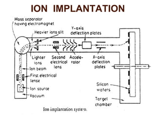
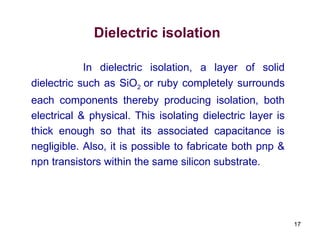
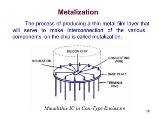
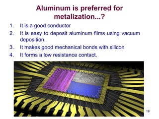
An integrated circuit consists of active and passive components fabricated together on a single crystal of silicon. It offers advantages like miniaturization, cost reduction, improved reliability and performance. The basic processes to fabricate monolithic ICs include silicon wafer preparation, epitaxial growth, oxidation, photolithography, diffusion, ion implantation, isolation techniques and metallization. Each process involves multiple steps to introduce impurities, create circuit patterns and interconnect components on a chip, which is then packaged.
In MOS, source-drain regions of adjacent MOS transistors together with interconnection metal lines may constitute parasitic MOS transistors unless they are isolated from each other. Hence, each MOSFET must be electrically isolated from each other. Device Isolation Techniques in VLSI microfabrication of MOS are discussed.
Semiconductor device fabrication is the process used to create the integrated circuits that are present in everyday electrical and electronic devices. It is a multiple-step sequence of photo lithographic and chemical processing steps during which electronic circuits are gradually created on a wafer made of pure semiconducting material. Silicon is almost always used, but various compound semiconductors are used for specialized applications.
1.Silicon Manufacturing
a) Czochralski method.
b) Wafer Manufacturing
c) Crystal structure
2.Photolithography
a) Photoresists
b) Photomask and Reticles
c) Patterning
1.Silicon Manufacturing
a) Czochralski method.
b) Wafer Manufacturing
c) Crystal structure
2.Photolithography
a) Photoresists
b) Photomask and Reticles
c) Patterning
MONOLITHIC IC PROCESSES A monolithic integrated circuit (IC) is a set of circuitry on a single semiconductor plate or chip rather than built of separate elements as a discrete circuit is.
This is one of the fabrication technology used in IC fabrication. This technique is mostly used in flexible electronics. It contains various other subprocesses in it.
Semiconductors are materials that have electrical conductivity between conductors such as most metals and nonconductors or insulators like ceramics. How much electricity a semiconductor can conduct depends on the material and its mixture content.
Semiconductors can be insulators at low temperatures and conductors at high temperatures. As they are used in the fabrication of electronic devices, semiconductors play an important role in our lives.
Acetabularia Information For Class 9 .docxvaibhavrinwa19
Acetabularia acetabulum is a single-celled green alga that in its vegetative state is morphologically differentiated into a basal rhizoid and an axially elongated stalk, which bears whorls of branching hairs. The single diploid nucleus resides in the rhizoid.
June 3, 2024 Anti-Semitism Letter Sent to MIT President Kornbluth and MIT Cor...Levi Shapiro
Letter from the Congress of the United States regarding Anti-Semitism sent June 3rd to MIT President Sally Kornbluth, MIT Corp Chair, Mark Gorenberg
Dear Dr. Kornbluth and Mr. Gorenberg,
The US House of Representatives is deeply concerned by ongoing and pervasive acts of antisemitic
harassment and intimidation at the Massachusetts Institute of Technology (MIT). Failing to act decisively to ensure a safe learning environment for all students would be a grave dereliction of your responsibilities as President of MIT and Chair of the MIT Corporation.
This Congress will not stand idly by and allow an environment hostile to Jewish students to persist. The House believes that your institution is in violation of Title VI of the Civil Rights Act, and the inability or
unwillingness to rectify this violation through action requires accountability.
Postsecondary education is a unique opportunity for students to learn and have their ideas and beliefs challenged. However, universities receiving hundreds of millions of federal funds annually have denied
students that opportunity and have been hijacked to become venues for the promotion of terrorism, antisemitic harassment and intimidation, unlawful encampments, and in some cases, assaults and riots.
The House of Representatives will not countenance the use of federal funds to indoctrinate students into hateful, antisemitic, anti-American supporters of terrorism. Investigations into campus antisemitism by the Committee on Education and the Workforce and the Committee on Ways and Means have been expanded into a Congress-wide probe across all relevant jurisdictions to address this national crisis. The undersigned Committees will conduct oversight into the use of federal funds at MIT and its learning environment under authorities granted to each Committee.
• The Committee on Education and the Workforce has been investigating your institution since December 7, 2023. The Committee has broad jurisdiction over postsecondary education, including its compliance with Title VI of the Civil Rights Act, campus safety concerns over disruptions to the learning environment, and the awarding of federal student aid under the Higher Education Act.
• The Committee on Oversight and Accountability is investigating the sources of funding and other support flowing to groups espousing pro-Hamas propaganda and engaged in antisemitic harassment and intimidation of students. The Committee on Oversight and Accountability is the principal oversight committee of the US House of Representatives and has broad authority to investigate “any matter” at “any time” under House Rule X.
• The Committee on Ways and Means has been investigating several universities since November 15, 2023, when the Committee held a hearing entitled From Ivory Towers to Dark Corners: Investigating the Nexus Between Antisemitism, Tax-Exempt Universities, and Terror Financing. The Committee followed the hearing with letters to those institutions on January 10, 202
The French Revolution, which began in 1789, was a period of radical social and political upheaval in France. It marked the decline of absolute monarchies, the rise of secular and democratic republics, and the eventual rise of Napoleon Bonaparte. This revolutionary period is crucial in understanding the transition from feudalism to modernity in Europe.
For more information, visit-www.vavaclasses.com
Model Attribute Check Company Auto PropertyCeline George
In Odoo, the multi-company feature allows you to manage multiple companies within a single Odoo database instance. Each company can have its own configurations while still sharing common resources such as products, customers, and suppliers.
A Strategic Approach: GenAI in EducationPeter Windle
Artificial Intelligence (AI) technologies such as Generative AI, Image Generators and Large Language Models have had a dramatic impact on teaching, learning and assessment over the past 18 months. The most immediate threat AI posed was to Academic Integrity with Higher Education Institutes (HEIs) focusing their efforts on combating the use of GenAI in assessment. Guidelines were developed for staff and students, policies put in place too. Innovative educators have forged paths in the use of Generative AI for teaching, learning and assessments leading to pockets of transformation springing up across HEIs, often with little or no top-down guidance, support or direction.
This Gasta posits a strategic approach to integrating AI into HEIs to prepare staff, students and the curriculum for an evolving world and workplace. We will highlight the advantages of working with these technologies beyond the realm of teaching, learning and assessment by considering prompt engineering skills, industry impact, curriculum changes, and the need for staff upskilling. In contrast, not engaging strategically with Generative AI poses risks, including falling behind peers, missed opportunities and failing to ensure our graduates remain employable. The rapid evolution of AI technologies necessitates a proactive and strategic approach if we are to remain relevant.
Welcome to TechSoup New Member Orientation and Q&A (May 2024).pdfTechSoup
In this webinar you will learn how your organization can access TechSoup's wide variety of product discount and donation programs. From hardware to software, we'll give you a tour of the tools available to help your nonprofit with productivity, collaboration, financial management, donor tracking, security, and more.
Read| The latest issue of The Challenger is here! We are thrilled to announce that our school paper has qualified for the NATIONAL SCHOOLS PRESS CONFERENCE (NSPC) 2024. Thank you for your unwavering support and trust. Dive into the stories that made us stand out!
Palestine last event orientationfvgnh .pptxRaedMohamed3
An EFL lesson about the current events in Palestine. It is intended to be for intermediate students who wish to increase their listening skills through a short lesson in power point.
Embracing GenAI - A Strategic ImperativePeter Windle
Artificial Intelligence (AI) technologies such as Generative AI, Image Generators and Large Language Models have had a dramatic impact on teaching, learning and assessment over the past 18 months. The most immediate threat AI posed was to Academic Integrity with Higher Education Institutes (HEIs) focusing their efforts on combating the use of GenAI in assessment. Guidelines were developed for staff and students, policies put in place too. Innovative educators have forged paths in the use of Generative AI for teaching, learning and assessments leading to pockets of transformation springing up across HEIs, often with little or no top-down guidance, support or direction.
This Gasta posits a strategic approach to integrating AI into HEIs to prepare staff, students and the curriculum for an evolving world and workplace. We will highlight the advantages of working with these technologies beyond the realm of teaching, learning and assessment by considering prompt engineering skills, industry impact, curriculum changes, and the need for staff upskilling. In contrast, not engaging strategically with Generative AI poses risks, including falling behind peers, missed opportunities and failing to ensure our graduates remain employable. The rapid evolution of AI technologies necessitates a proactive and strategic approach if we are to remain relevant.
3. ST 2014 3
An integrated circuit (IC) is a miniature ,low cost
electronic circuit consisting of active and passive components
fabricated together on a single crystal of silicon. The active
components are transistors and diodes and passive
components are resistors and capacitors.
INTEGRATED CIRCUITS
4. 4
Advantages of integrated circuits
1. Miniaturization and hence increased
equipment density.
2. Cost reduction due to batch processing.
3. Increased system reliability due to the
elimination of soldered joints.
4. Improved functional performance.
5. Matched devices.
6. Increased operating speeds.
7. Reduction in power consumption
7. 7
Epitaxial growth
1. Epitaxy means growing a single crystal silicon
structure upon a original silicon substrate, so that
the resulting layer is an extension of the substrate
crystal structure.
2. The basic chemical reaction in the epitaxial
growth process of pure silicon is the hydrogen
reduction of silicon tetrachloride.
1200o
C
SiCl+ 2H <-----------> Si + 4 HCl
8. 8
Oxidation
1. SiO2 is an extremely hard protective coating & is
unaffected by almost all reagents except by
hydrochloric acid. Thus it stands against any
contamination.
2. By selective etching of SiO2, diffusion of impurities
through carefully defined through windows in the
SiO2 can be accomplished to fabricate various
components.
9. 9
Oxidation
The silicon wafers are stacked up in a quartz boat & then
inserted into quartz furnace tube. The Si wafers are raised to
a high temperature in the range of 950 to 1150 o
C & at the
same time, exposed to a gas containing O2 or H2O or both.
The chemical action is Si + 2H2
O-----------> SiO2+ 2H2
10.
11. 11
Photolithography
The process of photolithography
makes it possible to produce microscopically
small circuit and device pattern on si wafer.
Two processes involved in photolithography
a) Making a photographic mask
b) Photo etching
12. 12
Photographic mask
The development of photographic mask
involves the preparation of initial artwork and its
diffusion, reduction, decomposition of initial
artwork or layout into several mask layers.
Photo etching
Photo etching is used for the removal of SiO2
from desired regions so that the desired
impurities can be diffused.
14. 14
Diffusion
The process of introducing impurities into selected
regions of a silicon wafer is called diffusion. The rate at
which various impurities diffuse into the silicon will be
of the order of 1µm/hr at the temperature range of 9000
C to 11000
C .The impurity atoms have the tendency to
move from regions of higher concentrations to lower
concentrations.
15. 15
Ion implantation technique
1. It is performed at low temperature. Therefore,
previously diffused regions have a lesser
tendency for lateral spreading.
2. In diffusion process, temperature has to be
controlled over a large area inside the oven,
where as in ion implantation process,
accelerating potential & beam content are
controlled from outside.
17. 17
Dielectric isolation
In dielectric isolation, a layer of solid
dielectric such as SiO2 or ruby completely surrounds
each components thereby producing isolation, both
electrical & physical. This isolating dielectric layer is
thick enough so that its associated capacitance is
negligible. Also, it is possible to fabricate both pnp &
npn transistors within the same silicon substrate.
18. 18
Metalization
The process of producing a thin metal film layer that
will serve to make interconnection of the various
components on the chip is called metalization.
19. 19
Aluminum is preferred for
metalization...?
1. It is a good conductor
2. It is easy to deposit aluminum films using vacuum
deposition.
3. It makes good mechanical bonds with silicon
4. It forms a low resistance contact.