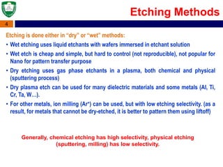
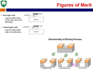
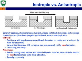
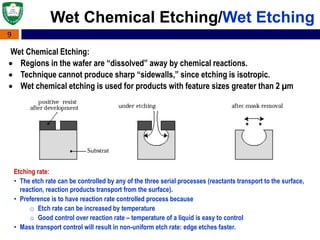
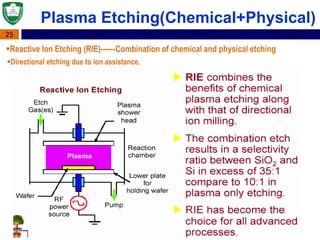
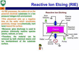
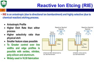
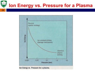
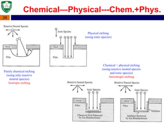
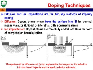
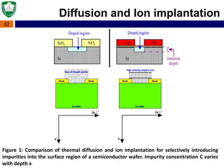
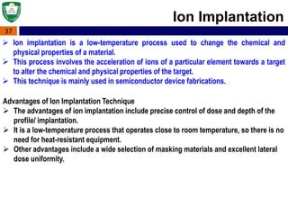
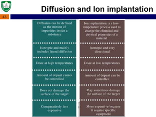
Etching
Diffusion & Ion Implantation
Instructor
Abu Syed Md. Jannatul Islam
Lecturer, Dept. of EEE, KUET, BD
1
Department of Electrical and Electronic Engineering
Khulna University of Engineering & Technology
Khulna-9203
2
Etching is the process where unwanted areas of
films are removed by either dissolving them in a
wet chemical solution (Wet Etching) or by reacting
them with gases in a plasma to form volatile
products (Dry Etching).
Resist protects areas which are to remain. In
some cases a hard mask, usually patterned layers
of SiO2 or Si3N4, are used when the etch selectivity
to photo-resist is low or the etching environment
causes resist to delaminate.
This is part of lithography - pattern transfer.
Etching
3
 To remove material from areas identified by the lithography process
 To create structures for functional use
 To remove oxide layers below features to allow for motion
Necessity of Etching
4
Etching is done either in “dry” or “wet” methods:
• Wet etching uses liquid etchants with wafers immersed in etchant solution
• Wet etch is cheap and simple, but hard to control (not reproducible), not popular for
Nano for pattern transfer purpose
• Dry etching uses gas phase etchants in a plasma, both chemical and physical
(sputtering process)
• Dry plasma etch can be used for many dielectric materials and some metals (Al, Ti,
Cr, Ta, W…).
• For other metals, ion milling (Ar+) can be used, but with low etching selectivity. (as a
result, for metals that cannot be dry-etched, it is better to pattern them using liftoff)
Generally, chemical etching has high selectivity, physical etching
(sputtering, milling) has low selectivity.
Etching Methods
5
Etching is consisted of 3 processes:
• Mass transport of reactants (through a boundary layer) to the surface to be etched
• Reaction between reactants and the film to be etched at the surface
• Mass transport of reaction products from the surface through the surface boundary
layer
Etching Basic
6
Figures of Merit
Blue: layer to remain
1. A poorly selective etch removes the top layer,
but also attacks the underlying material.
2. A highly selective etch leaves the underlying
material unharmed
Selectivity
Red: masking layer;
yellow: layer to be removed
1. A perfectly isotropic etch produces round
sidewalls.
2. A perfectly anisotropic etch produces vertical
sidewalls
Isotropy
7
Figures of Merit
8
Isotropic vs. Anisotropic
Generally speaking, chemical process (wet etch, plasma etch) leads to isotropic etch; whereas
physical process (directional energetic bombardment) leads to anisotropic etch.
Isotropic:
• Best to use with large features when sidewall slope does not matter, and to undercut the
mask (for easy liftoff).
• Large critical dimension (CD, i.e. feature size) loss, generally not for nano-fabrication.
• Quick, easy, and cheap.
Anisotropic:
• Best for making small features with vertical sidewalls, preferred pattern transfer method
for nano-fabrication and some micro-fabrication.
• Typically more costly.
9
Wet Chemical Etching:
 Regions in the wafer are “dissolved” away by chemical reactions.
 Technique cannot produce sharp “sidewalls,” since etching is isotropic.
 Wet chemical etching is used for products with feature sizes greater than 2 µm
Wet Chemical Etching/Wet Etching
Etching rate:
• The etch rate can be controlled by any of the three serial processes (reactants transport to the surface,
reaction, reaction products transport from the surface).
• Preference is to have reaction rate controlled process because
o Etch rate can be increased by temperature
o Good control over reaction rate – temperature of a liquid is easy to control
• Mass transport control will result in non-uniform etch rate: edge etches faster.
10
Wet Chemical Etching/Wet Etching
Advantages:
 Damage-free finish to wafer surface where surface morphology is typically smooth
and shiny
 Fast etch rate especially for blanket etch (μm/min)
 Etching is only chemical: great selectivity
 Simple and direct etching process since simple resist can be used as etch mask
 process occur at atmospheric environment
 Cheaper cost
 High etch selectivity easily available for etchants, resist and etched materials
 good etch uniformity across wafer
Disadvantages:
 Isotropic etching
 No control for precision etching
 Not well suited for nanostructures.
 Poor process control,
 Not well reproducible.
11
Application of Wet Process
Silicon etching:
For semiconductor materials, wet chemical etching usually proceed by oxidation
followed by the dissolution of the oxide by a chemical reaction.
For silicon, the most commonly used etchants are mixture of nitric acid (HNO3) and
hydrofluoric acid (HF) in water or acetic acid (CH3COOH)
Si + 4HNO3 → SiO2 + 2H2O + 4NO2
Hydrofluoric acid is used to dissolve the SiO2 layer
SiO2 +6HF → H2SiF6 + 2H2O
Silicon dioxide etching:
Dilute solution of HF with or without the addition of ammonium fluoride (NH4F) is used
for wet etching.
12
Silicon nitride and Poly-silicon Etching:
Silicon nitride films are etchable at room temperature in concentrated HF or buffered
HF and in a boiling H3PO4 solution.
Selective etching of nitride to oxide is done with 85% H3PO4 at 180oC because this
solution attacks silicon dioxide very slowly. Silicon rate for silicon nitride is 10nm/min
but less than 1nm/min for silicon dioxide
Gallium Arsenide Etching:
The most commonly used etchants are the H2SO4-H2O2-H2O and H3PO4-H2O2-H2O.
For an etchant with an 8:1:1 volume ration of H2SO4:H2O2-H2O, the etch rate is 0.8
µm/min for <111> Ga face and 1.5 µm/min for all other faces.
Application of Wet Process
13
In dry Etching, material removal reactions occur in the gas phase.
It can be plasma or non-plasma based.
Advantages
 Eliminates handling of dangerous acids and solvents
 Uses small amounts of chemicals
 Isotropic or anisotropic etch profiles
 Faithful pattern transfer into underlying layers (little feature size loss)
 Directional etching without using the crystal orientation of Si
 High resolution and cleanliness
 Less undercutting
 No unintentional prolongation of etching
 Better process control
 Ease of automation
Disadvantages:
 Some gases are quite toxic and corrosive
 Re-deposition of no volatile compounds
 Need for specialised expensive equipment
Dry Etching
14
Types of Dry Etching
• Non-plasma based - uses spontaneous reaction of appropriate reactive
gas mixture.
• Plasma based - uses radio frequency (RF) power to drive chemical
reaction.
15
15
Non-Plasma based Dry Etching
• XeF2 is a white powder, with vapor pressure
3.8 Torr at 25oC.
• Typical etch rate 1μm/min
• Heat is generated during exothermic reaction
2XeF2 + Si  2Xe (g) + SiF4 (g)
Popular for MEMS application.
Xenon di-fluoride (XeF2) etching of Si:
MEMS: micro electro mechanical systems
15
 Isotropic etching of Si
 Typically F-containing gases(fluorides or interhalogens) that readily etch Si
 High selectivity to masking layers
 No need for plasma processing equipment
 Highly controllable via temperature and partial pressure of reactants
16
What is a Plasma?
A plasma is a partially ionized gas made up of equal parts positively and negatively
charged particles.
Plasmas are generated by flowing gases through an electric or magnetic field.
Plasma consists of: ionized
atoms/molecules + free electrons,
free radicals (neutral).
Various reactions and species
present in a plasma
17
Plasma Etching
• Two components existed in plasma
o Ionic species results in directional etching.
o Chemical reactive species results in high etch selectivity.
• Control of the ratio of ionic/reactive components in plasma can modulate the dry
etching rate and etching profile.
18
Chemical
Process
Physical
Process
Wetetching
Plasmaetching
ReactiveIon
etching
Highdensityplasma
etching
Ionmilling&
Sputteretching
Pressure
Selectivity
Energy (power)
Anisotropicity
Plasma Etching Types
• Chemical etching: free radicals react with material to be removed. E.g. plasma etching at high
pressure close to 1Torr.
• Physical etching or sputtering: ionic species, accelerated by the built-in electric field (self-bias),
bombard the materials to be removed. E.g. sputter cleaning using Ar gas in sputter deposition
system.
• Ion enhanced etching: combined chemical and physical process, higher material removal rate
than each process alone. E.g. reactive ion etching (RIE), which is the most widely used dry
etching technique.
19
Plasma Etching(Chemical)
• In a plasma, reactive neutral chemical
species (free radicals, e.g. F atoms or
molecular species CF3) are mainly
responsible for the chemical reaction due
to their much greater numbers compared
to ions.
• Those free radicals are more abundant
than ions because:
1) they are generated at lower threshold
energy (e.g. < 8eV; in comparison, Ar is
ionized at 15.7eV); and
2) they (uncharged radicals) have longer
lifetime in the plasma.
• The neutral radicals arrive at cathode
surface by diffusion (thus non-
directional).
Due to their incomplete bonding,
free radicals are highly reactive
chemical species.
Chemical etching
20
• Due to their incomplete bonding (incomplete outer shells), free radicals (neutral,
e.g. CF3 and F from CF4 plasma) are highly reactive chemical species.
• Free radicals react with film to be etched and form volatile by-products.
Pure chemical etch is isotropic or nearly
isotropic, and the etching profile depends
on arrival angle and sticking coefficients
of free radicals.
Plasma Etching(Chemical)
21
Advantages:
 Lower chemical costs
 Reduced environmental impact
 Greater cleanliness
 Greater potential for production-line automation.
Disadvantages:
Plasma etch has lower selectivity than wet etching
Pure chemical etch is isotropic or nearly isotropic
High RF levels can cause damage to the wafer
Plasma Etching(Chemical)
22
Plasma Etching(Physical)
Physically bombard the films to be etched with energized chemically
inert ions or atoms
Material is removed by ion bombardment of the substrate. This
process is most often used to pre-clean substrates prior to deposition.
Gas discharge is used to energize chemically inert ions or atoms(e.g.
Ar)
 Highly anisotropic etching
Damage to underlying material—may change device properties
Rarely used in VLSI
23
Sputtering Etching/Ion Milling
• Physical milling when using heavy inert
gases (Ar).
• Plasma is used to generate ion beam (Ar+),
which is extracted and accelerated to etch
the sample. (i.e. sample outside of plasma)
• Thus the ion density (determined by plasma
source) and ion energy (determined by DC
acceleration voltage – bias by applied DC
voltage, not by RF bias as in high density
plasma etching system), can be controlled
independently.
• High acceleration voltage (>1kV), leading to
mill rate 10-30nm/min.
• Used whenever RIE is not possible (due to
the lack of volatile species formation).
Usually employed to etch Cu, Ni, Au,
superconducting materials containing
metals…
• Low pressure 10-4Torr (>1 order lower than
RIE), so large mean free path and less energy
loss due to collision. (such low pressure
cannot sustain a plasma, so ion milling is not
plasma etching)
24
Figure 10-8 Problems associated with sputter etching (or any etching that has a high
degree of physical/ionic etching): a) trenching at bottom of sidewalls; b) redeposition of
photoresist and other materials; c) charging and ion path distortion. 24
• Poor selectivity (2:1 or 1:1), very anisotropic.
• Sputtering rate depends on sputter yields which can be a function of incident angle.
• Problems include faceting (sputter yield is a function of incident angle), trenching, re-
deposition, charging and ion path distortion, radiation damage.
• Not popular, etches too slow, though reactive gas (CF4, CCl4, O2) can be added to slightly
improve selectivity and etching rate.
Sputtering Etching/Ion Milling
25
Reactive Ion Etching (RIE)------Combination of chemical and physical etching
Plasma Etching(Chemical+Physical)
Directional etching due to ion assistance.
26
In RIE processes, the wafers sit on the
powered electrode substrates in a low
pressure halogen-rich environment.
This placement sets up a negative
bias on the wafer which accelerates
positively charge ions(chemically inert
ions) toward the surface.
Moreover, glow discharge is used to
produce chemically reactive species
(atoms, radicals, or ions)
Therefore, the material can be
removed by both chemical means and
ion bombardment of the substrate
surface.
Reactive Ion Etcing (RIE)
27
• RIE is an anisotropic (due to directional ion bombardment) and highly selective (due to
chemical reaction) etching process.
 Anisotropic Profile
 Higher Etch Rate than either
process
 Higher selectivity ratio than
physical etch
 Smaller feature sizes possible
 To Greater control over line
widths and edge profiles is
possible with oxides, nitrides,
poly-silicon and aluminum.
 Widely used in VLSI fabrication
Reactive Ion Etcing (RIE)
28
Ion Energy vs. Pressure for a Plasma
29
Chemical—Physical---Chem.+Phys.
Purely chemical etching
(using only reactive
neutral species)
Isotropic etching
Chemical + physical etching
(using reactive neutral species
and ionic species)
Anisotropic etching
Physical etching
(using ionic species)
30
 Impurity doping is the introduction of controlled amount of impurity
dopant into semiconductors.
 The main goal of doping is changing the electrical properties of
semiconductor.
Importance of Doping
 Formation of p-n junction and fabrication of devices during wafer
fabrication.
 Alter the type and level of conductivity of semiconductor materials.
 Form bases, emitters, and resistors in bipolar devices, as well as
drains and sources in MOS devices.
 Dope poly-silicon layers.
Impurity Doping
31
 Diffusion and ion implantation are the two key methods of impurity
doping
 Diffusion: Dopant atoms move from the surface into Si by thermal
means via substitutional or interstitial diffusion mechanisms.
 Ion implantation: Dopant atoms are forcefully added into Si in the form
of energetic ion beam injection.
Comparison of (a) diffusion and (b) ion implantation techniques for the selective
introduction of dopants into the semiconductor substrate.
Doping Techniques
32
Figure 1: Comparison of thermal diffusion and ion implantation for selectively introducing
impurities into the surface region of a semiconductor wafer. Impurity concentration C varies
with depth x
Diffusion and Ion implantation
33
Dopant Sources
34
What is Diffusion?
Simple diffusion of a substance (blue) due to a concentration gradient across a semi-
permeable membrane (pink).
 Basically, the process happens as a result of the concentration
gradient.
 Diffusion process is carried out in systems called “diffusion furnaces”.
 It is fairly expensive and very accurate.
 There are three main sources of dopants: gaseous, liquid, and solids
 the gaseous sources are the one most widely used in this technique
(Reliable and convenient sources: BF3, PH3, AsH3).
 In this process, the source gas reacts with oxygen on the wafer surface
resulting in a dopant oxide. Next, it diffuses into Silicon, forming an
uniform dopant concentration across the surface.
35
Diffusion Steps
There are two main steps of diffusion as follows. These steps are used to create doped
regions.
Pre-deposition (for dose control)
In this step, desired dopant atoms are
controllably introduced on to the target from
methods such as gas phase diffusions, and
solid phase diffusions.
Drive-in (for profile control)
Once the dopant atoms have arrived on the wafer
surface, they need to be redistributed into the bulk.
This process is called drive-in. In this step, the
introduced dopants are driven deeper into the
substance without introducing further dopant
atoms.
36
Phosphorus Diffusion
Schematic diagram of a typical open tube
diffusion system
An example of the chemical reaction for phosphorus diffusion using a liquid source is
4POCl3 + 3O2 → 2P2O5 + 6Cl2
The P2O5 forms a glass on silicon wafer and is then reduced to phosphorus by silicon:
2P2O5 + 5Si → 4P + 5SiO2
The phosphorus is released and diffuse in to the silicon, and Cl2 is vented.
37
Ion Implantation
 Ion implantation is a low-temperature process used to change the chemical and
physical properties of a material.
 This process involves the acceleration of ions of a particular element towards a target
to alter the chemical and physical properties of the target.
 This technique is mainly used in semiconductor device fabrications.
Advantages of Ion Implantation Technique
 The advantages of ion implantation include precise control of dose and depth of the
profile/ implantation.
 It is a low-temperature process that operates close to room temperature, so there is no
need for heat-resistant equipment.
 Other advantages include a wide selection of masking materials and excellent lateral
dose uniformity.
38
Figure 17: Schematic of the ion implantation process. Dopant atoms are ionized by bombarding
with electrons. These are then isolated, accelerated, and then impinged on the wafer. There is
also a scanning system that allows the ion beam to scan over the wafer surface. Adapted from
Fundamentals of semiconductor manufacturing and process control - May and Spanos.
Ion Implantation Process
39
In ion implantation, dopant atoms are ionized, isolated, accelerated and
made to impinge on the wafer surface.
Ion implantation equipment should contain an ion source.
The source material is usually in the form of a gas e.g. AsH3, PH3, and
BF3 are some common sources.
Similarly, elemental sources like As and P are also used as solid
sources.
This ion source produces ions of the desired element.
The ions are then separated using a mass analyzer, which is a 90◦
magnet, which bends the ions depending on the mass.
After selection, the desired ions are then accelerated and made to
impinge on the wafer surface
Beam scanning or rastering is also possible using electric field coils to
deflect the ion beams.
These ions strike the target, which is the material to be implanted.
Ion Implantation Process
40
Each ion is either an atom or a molecule.
The penetration depth of the ions depend on their energy (changed by
the accelerating field).
The amount of ions implanted on the target is known as the dose.
However, since the current supplied for the implantation is small, the
dose that can be implanted at a given time period is also small.
Therefore this technique is used where smaller chemical changes are
required.
Ion Implantation Process
41
 One major application of ion implantation is the doping of semiconductors.
 Ion implantation is especially useful with device scaling.
 It can also be used to dope small regions.
 It is usually used later in the process flow when thermal budgets are tight and the high
temperature of thermal diffusion is not allowed.
The concentration profile for ion implantation is shown in figure 18. The maximum
concentration is at a certain depth below the surface, called range. In thermal diffusion,
the maximum concentration is at the surface and the concentration decreases with depth.
Ion Implantation Process
42
Effect of Ion Implantation
 In ion implantation, since the wafer surface is impacted by high energy
ions, it can cause damage by knocking Si atoms from their position,
causing local structural damage.
 This needs a post thermal annealing treatment to repair the damage.
There are two ways of doing this.
1. Tube furnace - low temperature annealing (600-1000 ◦C). To minimize
lateral diffusion.
2. Rapid thermal annealing - higher temperatures are possible but for
shorter times.
43
Diffusion and Ion implantation

Etching, Diffusion, Ion Implantation--ABU SYED KUET

  • 1.
    Etching Diffusion & IonImplantation Instructor Abu Syed Md. Jannatul Islam Lecturer, Dept. of EEE, KUET, BD 1 Department of Electrical and Electronic Engineering Khulna University of Engineering & Technology Khulna-9203
  • 2.
    2 Etching is theprocess where unwanted areas of films are removed by either dissolving them in a wet chemical solution (Wet Etching) or by reacting them with gases in a plasma to form volatile products (Dry Etching). Resist protects areas which are to remain. In some cases a hard mask, usually patterned layers of SiO2 or Si3N4, are used when the etch selectivity to photo-resist is low or the etching environment causes resist to delaminate. This is part of lithography - pattern transfer. Etching
  • 3.
    3  To removematerial from areas identified by the lithography process  To create structures for functional use  To remove oxide layers below features to allow for motion Necessity of Etching
  • 4.
    4 Etching is doneeither in “dry” or “wet” methods: • Wet etching uses liquid etchants with wafers immersed in etchant solution • Wet etch is cheap and simple, but hard to control (not reproducible), not popular for Nano for pattern transfer purpose • Dry etching uses gas phase etchants in a plasma, both chemical and physical (sputtering process) • Dry plasma etch can be used for many dielectric materials and some metals (Al, Ti, Cr, Ta, W…). • For other metals, ion milling (Ar+) can be used, but with low etching selectivity. (as a result, for metals that cannot be dry-etched, it is better to pattern them using liftoff) Generally, chemical etching has high selectivity, physical etching (sputtering, milling) has low selectivity. Etching Methods
  • 5.
    5 Etching is consistedof 3 processes: • Mass transport of reactants (through a boundary layer) to the surface to be etched • Reaction between reactants and the film to be etched at the surface • Mass transport of reaction products from the surface through the surface boundary layer Etching Basic
  • 6.
    6 Figures of Merit Blue:layer to remain 1. A poorly selective etch removes the top layer, but also attacks the underlying material. 2. A highly selective etch leaves the underlying material unharmed Selectivity Red: masking layer; yellow: layer to be removed 1. A perfectly isotropic etch produces round sidewalls. 2. A perfectly anisotropic etch produces vertical sidewalls Isotropy
  • 7.
  • 8.
    8 Isotropic vs. Anisotropic Generallyspeaking, chemical process (wet etch, plasma etch) leads to isotropic etch; whereas physical process (directional energetic bombardment) leads to anisotropic etch. Isotropic: • Best to use with large features when sidewall slope does not matter, and to undercut the mask (for easy liftoff). • Large critical dimension (CD, i.e. feature size) loss, generally not for nano-fabrication. • Quick, easy, and cheap. Anisotropic: • Best for making small features with vertical sidewalls, preferred pattern transfer method for nano-fabrication and some micro-fabrication. • Typically more costly.
  • 9.
    9 Wet Chemical Etching: Regions in the wafer are “dissolved” away by chemical reactions.  Technique cannot produce sharp “sidewalls,” since etching is isotropic.  Wet chemical etching is used for products with feature sizes greater than 2 µm Wet Chemical Etching/Wet Etching Etching rate: • The etch rate can be controlled by any of the three serial processes (reactants transport to the surface, reaction, reaction products transport from the surface). • Preference is to have reaction rate controlled process because o Etch rate can be increased by temperature o Good control over reaction rate – temperature of a liquid is easy to control • Mass transport control will result in non-uniform etch rate: edge etches faster.
  • 10.
    10 Wet Chemical Etching/WetEtching Advantages:  Damage-free finish to wafer surface where surface morphology is typically smooth and shiny  Fast etch rate especially for blanket etch (μm/min)  Etching is only chemical: great selectivity  Simple and direct etching process since simple resist can be used as etch mask  process occur at atmospheric environment  Cheaper cost  High etch selectivity easily available for etchants, resist and etched materials  good etch uniformity across wafer Disadvantages:  Isotropic etching  No control for precision etching  Not well suited for nanostructures.  Poor process control,  Not well reproducible.
  • 11.
    11 Application of WetProcess Silicon etching: For semiconductor materials, wet chemical etching usually proceed by oxidation followed by the dissolution of the oxide by a chemical reaction. For silicon, the most commonly used etchants are mixture of nitric acid (HNO3) and hydrofluoric acid (HF) in water or acetic acid (CH3COOH) Si + 4HNO3 → SiO2 + 2H2O + 4NO2 Hydrofluoric acid is used to dissolve the SiO2 layer SiO2 +6HF → H2SiF6 + 2H2O Silicon dioxide etching: Dilute solution of HF with or without the addition of ammonium fluoride (NH4F) is used for wet etching.
  • 12.
    12 Silicon nitride andPoly-silicon Etching: Silicon nitride films are etchable at room temperature in concentrated HF or buffered HF and in a boiling H3PO4 solution. Selective etching of nitride to oxide is done with 85% H3PO4 at 180oC because this solution attacks silicon dioxide very slowly. Silicon rate for silicon nitride is 10nm/min but less than 1nm/min for silicon dioxide Gallium Arsenide Etching: The most commonly used etchants are the H2SO4-H2O2-H2O and H3PO4-H2O2-H2O. For an etchant with an 8:1:1 volume ration of H2SO4:H2O2-H2O, the etch rate is 0.8 µm/min for <111> Ga face and 1.5 µm/min for all other faces. Application of Wet Process
  • 13.
    13 In dry Etching,material removal reactions occur in the gas phase. It can be plasma or non-plasma based. Advantages  Eliminates handling of dangerous acids and solvents  Uses small amounts of chemicals  Isotropic or anisotropic etch profiles  Faithful pattern transfer into underlying layers (little feature size loss)  Directional etching without using the crystal orientation of Si  High resolution and cleanliness  Less undercutting  No unintentional prolongation of etching  Better process control  Ease of automation Disadvantages:  Some gases are quite toxic and corrosive  Re-deposition of no volatile compounds  Need for specialised expensive equipment Dry Etching
  • 14.
    14 Types of DryEtching • Non-plasma based - uses spontaneous reaction of appropriate reactive gas mixture. • Plasma based - uses radio frequency (RF) power to drive chemical reaction.
  • 15.
    15 15 Non-Plasma based DryEtching • XeF2 is a white powder, with vapor pressure 3.8 Torr at 25oC. • Typical etch rate 1μm/min • Heat is generated during exothermic reaction 2XeF2 + Si  2Xe (g) + SiF4 (g) Popular for MEMS application. Xenon di-fluoride (XeF2) etching of Si: MEMS: micro electro mechanical systems 15  Isotropic etching of Si  Typically F-containing gases(fluorides or interhalogens) that readily etch Si  High selectivity to masking layers  No need for plasma processing equipment  Highly controllable via temperature and partial pressure of reactants
  • 16.
    16 What is aPlasma? A plasma is a partially ionized gas made up of equal parts positively and negatively charged particles. Plasmas are generated by flowing gases through an electric or magnetic field. Plasma consists of: ionized atoms/molecules + free electrons, free radicals (neutral). Various reactions and species present in a plasma
  • 17.
    17 Plasma Etching • Twocomponents existed in plasma o Ionic species results in directional etching. o Chemical reactive species results in high etch selectivity. • Control of the ratio of ionic/reactive components in plasma can modulate the dry etching rate and etching profile.
  • 18.
    18 Chemical Process Physical Process Wetetching Plasmaetching ReactiveIon etching Highdensityplasma etching Ionmilling& Sputteretching Pressure Selectivity Energy (power) Anisotropicity Plasma EtchingTypes • Chemical etching: free radicals react with material to be removed. E.g. plasma etching at high pressure close to 1Torr. • Physical etching or sputtering: ionic species, accelerated by the built-in electric field (self-bias), bombard the materials to be removed. E.g. sputter cleaning using Ar gas in sputter deposition system. • Ion enhanced etching: combined chemical and physical process, higher material removal rate than each process alone. E.g. reactive ion etching (RIE), which is the most widely used dry etching technique.
  • 19.
    19 Plasma Etching(Chemical) • Ina plasma, reactive neutral chemical species (free radicals, e.g. F atoms or molecular species CF3) are mainly responsible for the chemical reaction due to their much greater numbers compared to ions. • Those free radicals are more abundant than ions because: 1) they are generated at lower threshold energy (e.g. < 8eV; in comparison, Ar is ionized at 15.7eV); and 2) they (uncharged radicals) have longer lifetime in the plasma. • The neutral radicals arrive at cathode surface by diffusion (thus non- directional). Due to their incomplete bonding, free radicals are highly reactive chemical species. Chemical etching
  • 20.
    20 • Due totheir incomplete bonding (incomplete outer shells), free radicals (neutral, e.g. CF3 and F from CF4 plasma) are highly reactive chemical species. • Free radicals react with film to be etched and form volatile by-products. Pure chemical etch is isotropic or nearly isotropic, and the etching profile depends on arrival angle and sticking coefficients of free radicals. Plasma Etching(Chemical)
  • 21.
    21 Advantages:  Lower chemicalcosts  Reduced environmental impact  Greater cleanliness  Greater potential for production-line automation. Disadvantages: Plasma etch has lower selectivity than wet etching Pure chemical etch is isotropic or nearly isotropic High RF levels can cause damage to the wafer Plasma Etching(Chemical)
  • 22.
    22 Plasma Etching(Physical) Physically bombardthe films to be etched with energized chemically inert ions or atoms Material is removed by ion bombardment of the substrate. This process is most often used to pre-clean substrates prior to deposition. Gas discharge is used to energize chemically inert ions or atoms(e.g. Ar)  Highly anisotropic etching Damage to underlying material—may change device properties Rarely used in VLSI
  • 23.
    23 Sputtering Etching/Ion Milling •Physical milling when using heavy inert gases (Ar). • Plasma is used to generate ion beam (Ar+), which is extracted and accelerated to etch the sample. (i.e. sample outside of plasma) • Thus the ion density (determined by plasma source) and ion energy (determined by DC acceleration voltage – bias by applied DC voltage, not by RF bias as in high density plasma etching system), can be controlled independently. • High acceleration voltage (>1kV), leading to mill rate 10-30nm/min. • Used whenever RIE is not possible (due to the lack of volatile species formation). Usually employed to etch Cu, Ni, Au, superconducting materials containing metals… • Low pressure 10-4Torr (>1 order lower than RIE), so large mean free path and less energy loss due to collision. (such low pressure cannot sustain a plasma, so ion milling is not plasma etching)
  • 24.
    24 Figure 10-8 Problemsassociated with sputter etching (or any etching that has a high degree of physical/ionic etching): a) trenching at bottom of sidewalls; b) redeposition of photoresist and other materials; c) charging and ion path distortion. 24 • Poor selectivity (2:1 or 1:1), very anisotropic. • Sputtering rate depends on sputter yields which can be a function of incident angle. • Problems include faceting (sputter yield is a function of incident angle), trenching, re- deposition, charging and ion path distortion, radiation damage. • Not popular, etches too slow, though reactive gas (CF4, CCl4, O2) can be added to slightly improve selectivity and etching rate. Sputtering Etching/Ion Milling
  • 25.
    25 Reactive Ion Etching(RIE)------Combination of chemical and physical etching Plasma Etching(Chemical+Physical) Directional etching due to ion assistance.
  • 26.
    26 In RIE processes,the wafers sit on the powered electrode substrates in a low pressure halogen-rich environment. This placement sets up a negative bias on the wafer which accelerates positively charge ions(chemically inert ions) toward the surface. Moreover, glow discharge is used to produce chemically reactive species (atoms, radicals, or ions) Therefore, the material can be removed by both chemical means and ion bombardment of the substrate surface. Reactive Ion Etcing (RIE)
  • 27.
    27 • RIE isan anisotropic (due to directional ion bombardment) and highly selective (due to chemical reaction) etching process.  Anisotropic Profile  Higher Etch Rate than either process  Higher selectivity ratio than physical etch  Smaller feature sizes possible  To Greater control over line widths and edge profiles is possible with oxides, nitrides, poly-silicon and aluminum.  Widely used in VLSI fabrication Reactive Ion Etcing (RIE)
  • 28.
    28 Ion Energy vs.Pressure for a Plasma
  • 29.
    29 Chemical—Physical---Chem.+Phys. Purely chemical etching (usingonly reactive neutral species) Isotropic etching Chemical + physical etching (using reactive neutral species and ionic species) Anisotropic etching Physical etching (using ionic species)
  • 30.
    30  Impurity dopingis the introduction of controlled amount of impurity dopant into semiconductors.  The main goal of doping is changing the electrical properties of semiconductor. Importance of Doping  Formation of p-n junction and fabrication of devices during wafer fabrication.  Alter the type and level of conductivity of semiconductor materials.  Form bases, emitters, and resistors in bipolar devices, as well as drains and sources in MOS devices.  Dope poly-silicon layers. Impurity Doping
  • 31.
    31  Diffusion andion implantation are the two key methods of impurity doping  Diffusion: Dopant atoms move from the surface into Si by thermal means via substitutional or interstitial diffusion mechanisms.  Ion implantation: Dopant atoms are forcefully added into Si in the form of energetic ion beam injection. Comparison of (a) diffusion and (b) ion implantation techniques for the selective introduction of dopants into the semiconductor substrate. Doping Techniques
  • 32.
    32 Figure 1: Comparisonof thermal diffusion and ion implantation for selectively introducing impurities into the surface region of a semiconductor wafer. Impurity concentration C varies with depth x Diffusion and Ion implantation
  • 33.
  • 34.
    34 What is Diffusion? Simplediffusion of a substance (blue) due to a concentration gradient across a semi- permeable membrane (pink).  Basically, the process happens as a result of the concentration gradient.  Diffusion process is carried out in systems called “diffusion furnaces”.  It is fairly expensive and very accurate.  There are three main sources of dopants: gaseous, liquid, and solids  the gaseous sources are the one most widely used in this technique (Reliable and convenient sources: BF3, PH3, AsH3).  In this process, the source gas reacts with oxygen on the wafer surface resulting in a dopant oxide. Next, it diffuses into Silicon, forming an uniform dopant concentration across the surface.
  • 35.
    35 Diffusion Steps There aretwo main steps of diffusion as follows. These steps are used to create doped regions. Pre-deposition (for dose control) In this step, desired dopant atoms are controllably introduced on to the target from methods such as gas phase diffusions, and solid phase diffusions. Drive-in (for profile control) Once the dopant atoms have arrived on the wafer surface, they need to be redistributed into the bulk. This process is called drive-in. In this step, the introduced dopants are driven deeper into the substance without introducing further dopant atoms.
  • 36.
    36 Phosphorus Diffusion Schematic diagramof a typical open tube diffusion system An example of the chemical reaction for phosphorus diffusion using a liquid source is 4POCl3 + 3O2 → 2P2O5 + 6Cl2 The P2O5 forms a glass on silicon wafer and is then reduced to phosphorus by silicon: 2P2O5 + 5Si → 4P + 5SiO2 The phosphorus is released and diffuse in to the silicon, and Cl2 is vented.
  • 37.
    37 Ion Implantation  Ionimplantation is a low-temperature process used to change the chemical and physical properties of a material.  This process involves the acceleration of ions of a particular element towards a target to alter the chemical and physical properties of the target.  This technique is mainly used in semiconductor device fabrications. Advantages of Ion Implantation Technique  The advantages of ion implantation include precise control of dose and depth of the profile/ implantation.  It is a low-temperature process that operates close to room temperature, so there is no need for heat-resistant equipment.  Other advantages include a wide selection of masking materials and excellent lateral dose uniformity.
  • 38.
    38 Figure 17: Schematicof the ion implantation process. Dopant atoms are ionized by bombarding with electrons. These are then isolated, accelerated, and then impinged on the wafer. There is also a scanning system that allows the ion beam to scan over the wafer surface. Adapted from Fundamentals of semiconductor manufacturing and process control - May and Spanos. Ion Implantation Process
  • 39.
    39 In ion implantation,dopant atoms are ionized, isolated, accelerated and made to impinge on the wafer surface. Ion implantation equipment should contain an ion source. The source material is usually in the form of a gas e.g. AsH3, PH3, and BF3 are some common sources. Similarly, elemental sources like As and P are also used as solid sources. This ion source produces ions of the desired element. The ions are then separated using a mass analyzer, which is a 90◦ magnet, which bends the ions depending on the mass. After selection, the desired ions are then accelerated and made to impinge on the wafer surface Beam scanning or rastering is also possible using electric field coils to deflect the ion beams. These ions strike the target, which is the material to be implanted. Ion Implantation Process
  • 40.
    40 Each ion iseither an atom or a molecule. The penetration depth of the ions depend on their energy (changed by the accelerating field). The amount of ions implanted on the target is known as the dose. However, since the current supplied for the implantation is small, the dose that can be implanted at a given time period is also small. Therefore this technique is used where smaller chemical changes are required. Ion Implantation Process
  • 41.
    41  One majorapplication of ion implantation is the doping of semiconductors.  Ion implantation is especially useful with device scaling.  It can also be used to dope small regions.  It is usually used later in the process flow when thermal budgets are tight and the high temperature of thermal diffusion is not allowed. The concentration profile for ion implantation is shown in figure 18. The maximum concentration is at a certain depth below the surface, called range. In thermal diffusion, the maximum concentration is at the surface and the concentration decreases with depth. Ion Implantation Process
  • 42.
    42 Effect of IonImplantation  In ion implantation, since the wafer surface is impacted by high energy ions, it can cause damage by knocking Si atoms from their position, causing local structural damage.  This needs a post thermal annealing treatment to repair the damage. There are two ways of doing this. 1. Tube furnace - low temperature annealing (600-1000 ◦C). To minimize lateral diffusion. 2. Rapid thermal annealing - higher temperatures are possible but for shorter times.
  • 43.

Editor's Notes

  • #25 Ion Beam Milling : Ions beam is used to “chisel”off material from a wafer. The process is physical rather than chemical. Feature sizes < 0.1 µm can be produced Sputtering (Ion Milling or Ion Beam Etch) Reduced pressure environment (<50 mTorr) Increases mean free path between molecules Fewer collisions between molecules Inert gas injected at low pressure is used as “milling” tool