Downloaded 133 times
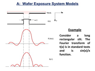
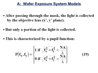
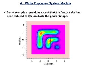
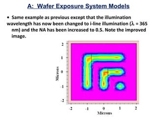
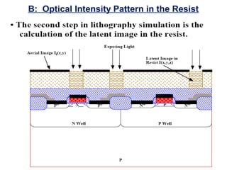
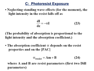
![B: Optical Intensity Pattern in the Resist
• Example of calculation of light intensity distribution in a photoresist layer
during exposure using the ATHENA simulator. A simple structure is defined
with a photoresist layer covering a silicon substrate which has two flat regions
and a sloped sidewall.
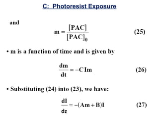
The simulation shows the
[PAC] calculated
concentration after an
exposure of 200 mJ cm-2
.
Lower [PAC] values
correspond to more
exposure. The color
contours thus
correspond to the
integrated light intensity
from the exposure.](https://image.slidesharecdn.com/5-140603091155-phpapp02/85/5-2-lithography-3-4-5-final-2013-44-320.jpg)
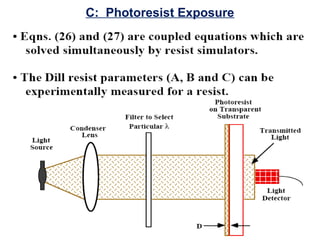
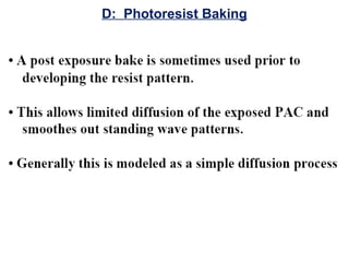
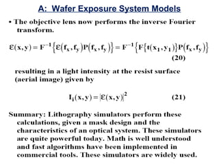
![D: Photoresist Baking
• Same simulation example as last one except that a post exposure bake of 45
minutes at 115 °C has now been included. The color contours again
correspond to the [PAC] after exposure. Note that the standing wave effects
apparent earlier have been “smeared out” by this bake, producing a more
uniform [PAC] distribution.](https://image.slidesharecdn.com/5-140603091155-phpapp02/85/5-2-lithography-3-4-5-final-2013-50-320.jpg)
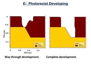


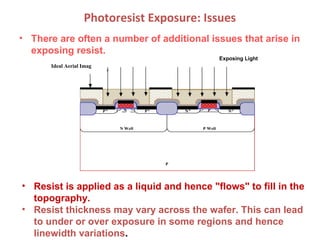
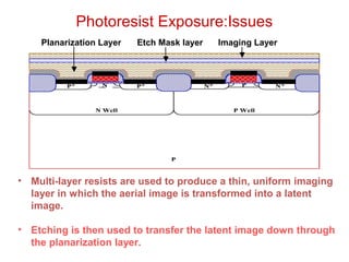
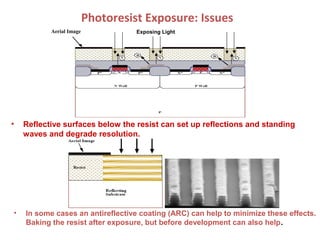
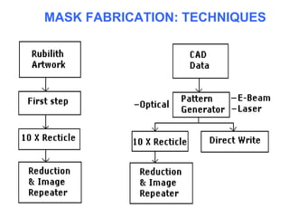
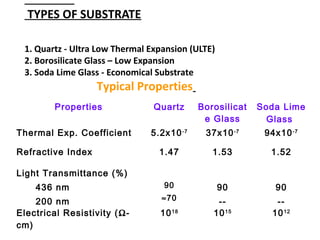
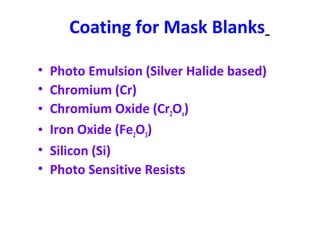
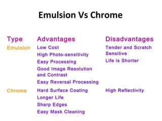
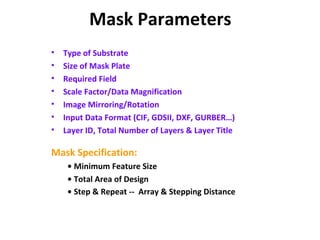
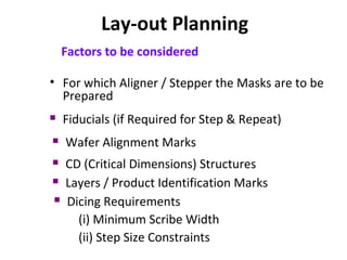
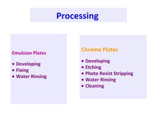
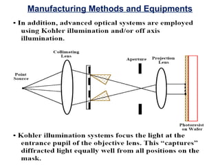
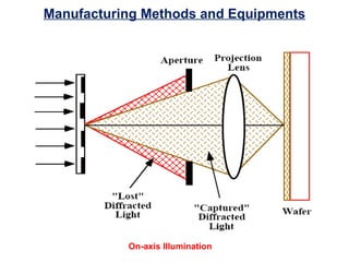
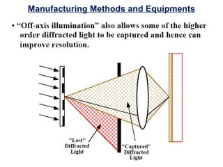
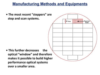
This document discusses various topics related to photolithography including: - Issues that can arise when exposing photoresist such as resist flowing, thickness variations, and reflections causing standing waves. - The use of multi-layer resists and etching to produce a uniform imaging layer. - Techniques for fabricating masks including the use of quartz, borosilicate glass, or soda lime glass substrates and coating materials like photoemulsion or chromium. - Inspection and quality control of fabricated masks. - Lithography simulation tools based on optical and resist chemistry models to simulate the aerial image and latent image formation.