Downloaded 768 times

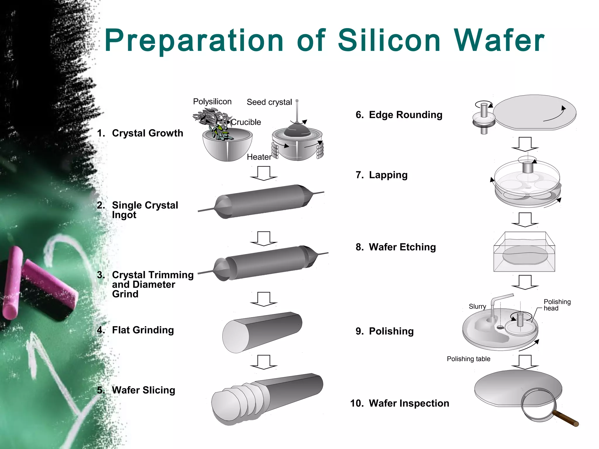


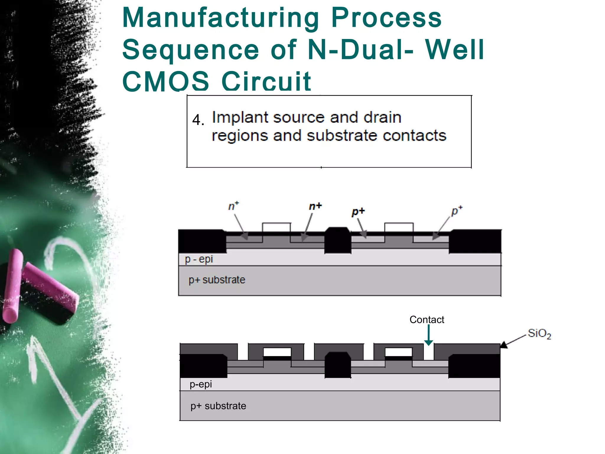


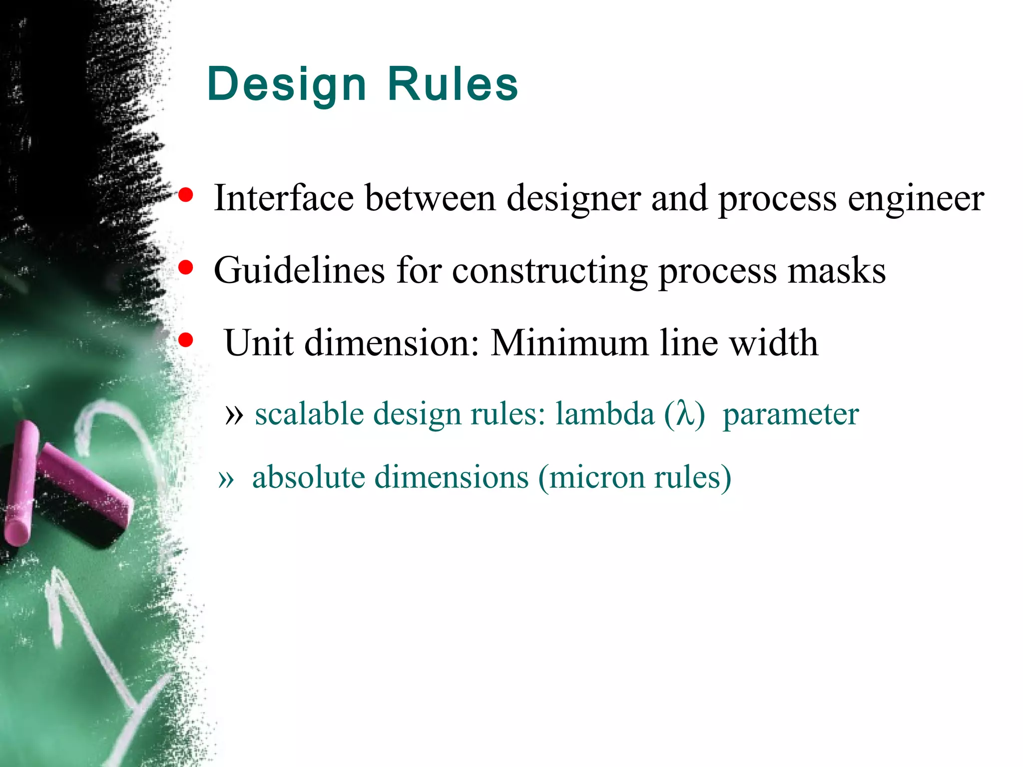


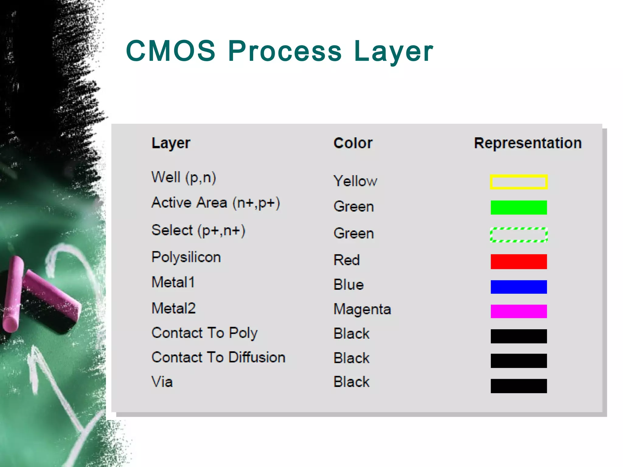
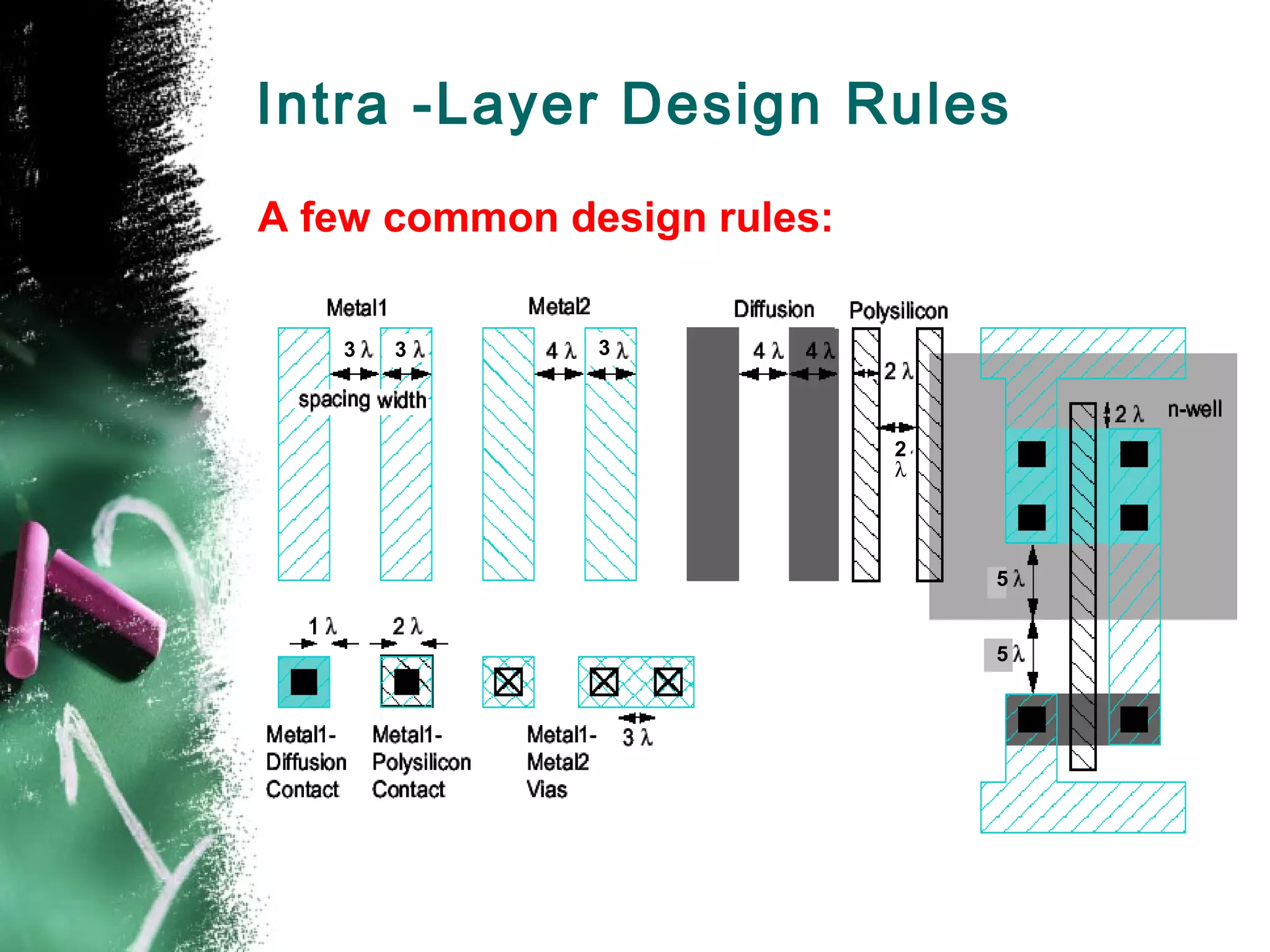


The document discusses the manufacturing process for CMOS integrated circuits. It describes the key steps which include wafer preparation, oxidation, diffusion, ion implantation, deposition, etching, and planarization. It emphasizes that design rules must be followed to ensure the functionality of the final circuit, as they define the minimum allowed dimensions and act as an agreement between designers and process engineers.


