Downloaded 36 times

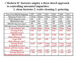
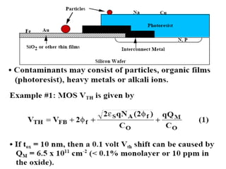
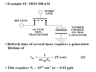
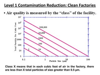
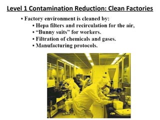
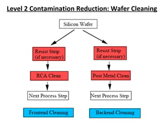
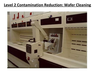
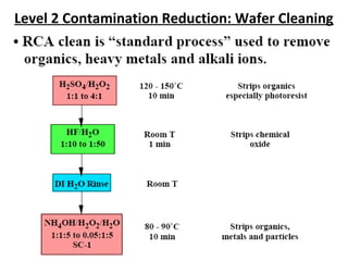
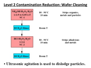
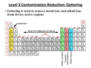
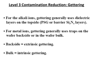
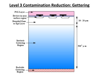
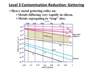
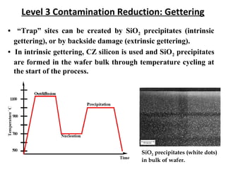
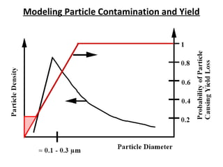
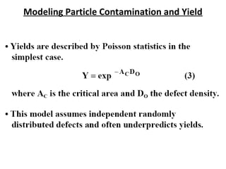
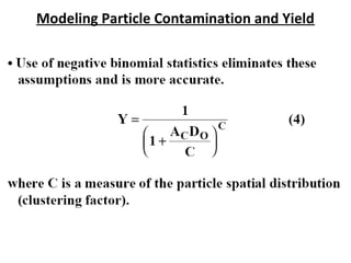
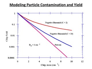
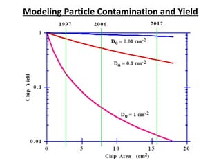

The document discusses three levels of contamination reduction in semiconductor manufacturing: Level 1 involves keeping clean rooms free of particles through strict air purity standards. Level 2 is wafer cleaning to remove unwanted contaminants from wafer surfaces. Level 3 is gettering, where silicon dioxide precipitates or damage to wafer backs effectively "trap" contaminant particles within the wafer bulk. Gettering helps prevent particles from reaching the device layer. The document also models how particle contamination affects yield and the need for extremely low defect densities with future technology nodes.