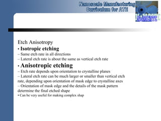
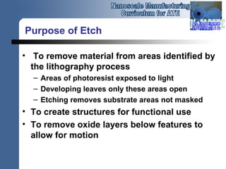
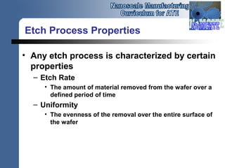
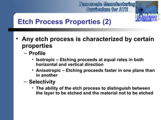
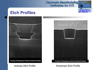
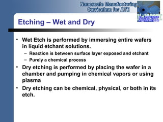
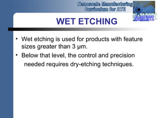
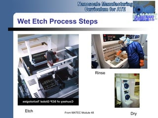
Top Down Method
Etch Processes
•In order to form a functional MEMS(Micro-Electro-Mechanical
Systems) structure on a substrate, it is necessary to etch the
thin films previously deposited.
Etch Anisotropy
• Isotropic etching
– Same etch rate in all directions
– Lateral etch rate is about the same as vertical etch rate
• Anisotropic etching
– Etch rate depends upon orientation to crystalline planes
– Lateral etch rate can be much larger or smaller than vertical etch
rate, depending upon orientation of mask edge to crystalline axes
– Orientation of mask edge and the details of the mask pattern
determine the final etched shape
• Can be very useful for making complex shap
Purpose of Etch
• To remove material from areas identified by
the lithography process
– Areas of photoresist exposed to light
– Developing leaves only these areas open
– Etching removes substrate areas not masked
• To create structures for functional use
• To remove oxide layers below features to
allow for motion
Etch Process Properties
• Any etch process is characterized by certain
properties
– Etch Rate
• The amount of material removed from the wafer over a
defined period of time
– Uniformity
• The evenness of the removal over the entire surface of
the wafer
Etch Process Properties (2)
• Any etch process is characterized by certain
properties
– Profile
• Isotropic – Etching proceeds at equal rates in both
horizontal and vertical direction
• Anisotropic – Etching proceeds faster in one plane than
in another
– Selectivity
• The ability of the etch process to distinguish between
the layer to be etched and the material not to be etched
Etch Profiles
Isotropic Etch Profile Anisotropic Etch Profile
Wet Etch Chemistries
• Layer Etchant
• Photoresist H2SO4, H2O2
• SiO2 HF, NH4F-HCl-NH4F
• Si3N4 ?, HNO3
• Si HF
Etching – Wet and Dry
• Wet Etch is performed by immersing entire wafers
in liquid etchant solutions.
– Reaction is between surface layer exposed and etchant
– Purely a chemical process
• Dry etching is performed by placing the wafer in a
chamber and pumping in chemical vapors or using
plasma
• Dry etching can be chemical, physical, or both in its
etch.
WET ETCHING
• Wet etching is used for products with feature
sizes greater than 3 μm.
• Below that level, the control and precision
needed requires dry-etching techniques.
Wet Etch
• Oxidation-reduction equations often define
wet etch processes
– Silicon etch with HNO3 & HF
• Si + HNO3 & HF → H2SiF6 + HNO2 + 2H2O
• Most Wet Etch Processes are Isotropic
– Etch proceeds in both vertical and horizontal
direction
– Etch mixtures can change the etch rate or profile
depending on silicon crystal orientation
Wet Etch Process Steps
From MATEC Module 48
Etch
Rinse
Dry
Wet Etch (2)
• Wet Etch processes can be batch processes
where multiple wafers are etched at one
time
• Wet etch processes are limited to feature
sizes of 3uM or larger, limiting their use in
nanomanufacturing to bulk processes
• Wet etch can be used to remove sacrificial
layers present in MEMS devices
• Wet etch is also used for resist stripping
Some Problems
• In complete & overcutting
Advantages & Disadvantages:
• Cheap, almost no damage due to purely
chemical nature, highly selective
• but
• poor anisotropy, poor process control
(temperature sensitivity), poor particle control,
Sources and References
[1] Xaio, Hong (2001). Introduction to Semiconductor Manufacturing Technology Prentice-Hall,
Upper Saddle River, NJ
[2] Van Zant, P. (1997). Microchip Fabrication, (3rd
ed.). McGraw-Hill.
[3] The Texas Engineering Extension Service, (1996). Semiconductor Processing Overview, Texas A&M
University System, p. 139-153..
[4] “Silicon Sacrificial Dry Layer Etching (SSLDE) for Free Standing RF MEMS architectures” S. Federico,
C. Hilbert, et al., 2004, http://cmi.epfl.ch/etch/MEMS03.pdf
[5] Maricopa Advanced Technology Education Center (2001) Module 47 “The Etch Process”
[6] Elliot, D. Integrated Circuit Fabrication Technology, McGraw-Hill, New York, 1996 p.282
[7] Bhattacharaya, R. and Reis, A(2004) “Deep Reactive Ion Etching”, University of Maryland,
http://www.ece.umd.edu/courses/enee416.S2004/presentation6.pdf
[8] Van Zant, P. (2004) Microchip Fabrication (4th
Edition) McGraw-Hill, New York

wet etching

  • 1.
    Top Down Method EtchProcesses •In order to form a functional MEMS(Micro-Electro-Mechanical Systems) structure on a substrate, it is necessary to etch the thin films previously deposited.
  • 2.
    Etch Anisotropy • Isotropicetching – Same etch rate in all directions – Lateral etch rate is about the same as vertical etch rate • Anisotropic etching – Etch rate depends upon orientation to crystalline planes – Lateral etch rate can be much larger or smaller than vertical etch rate, depending upon orientation of mask edge to crystalline axes – Orientation of mask edge and the details of the mask pattern determine the final etched shape • Can be very useful for making complex shap
  • 3.
    Purpose of Etch •To remove material from areas identified by the lithography process – Areas of photoresist exposed to light – Developing leaves only these areas open – Etching removes substrate areas not masked • To create structures for functional use • To remove oxide layers below features to allow for motion
  • 4.
    Etch Process Properties •Any etch process is characterized by certain properties – Etch Rate • The amount of material removed from the wafer over a defined period of time – Uniformity • The evenness of the removal over the entire surface of the wafer
  • 5.
    Etch Process Properties(2) • Any etch process is characterized by certain properties – Profile • Isotropic – Etching proceeds at equal rates in both horizontal and vertical direction • Anisotropic – Etching proceeds faster in one plane than in another – Selectivity • The ability of the etch process to distinguish between the layer to be etched and the material not to be etched
  • 6.
    Etch Profiles Isotropic EtchProfile Anisotropic Etch Profile
  • 7.
    Wet Etch Chemistries •Layer Etchant • Photoresist H2SO4, H2O2 • SiO2 HF, NH4F-HCl-NH4F • Si3N4 ?, HNO3 • Si HF
  • 8.
    Etching – Wetand Dry • Wet Etch is performed by immersing entire wafers in liquid etchant solutions. – Reaction is between surface layer exposed and etchant – Purely a chemical process • Dry etching is performed by placing the wafer in a chamber and pumping in chemical vapors or using plasma • Dry etching can be chemical, physical, or both in its etch.
  • 9.
    WET ETCHING • Wetetching is used for products with feature sizes greater than 3 μm. • Below that level, the control and precision needed requires dry-etching techniques.
  • 10.
    Wet Etch • Oxidation-reductionequations often define wet etch processes – Silicon etch with HNO3 & HF • Si + HNO3 & HF → H2SiF6 + HNO2 + 2H2O • Most Wet Etch Processes are Isotropic – Etch proceeds in both vertical and horizontal direction – Etch mixtures can change the etch rate or profile depending on silicon crystal orientation
  • 11.
    Wet Etch ProcessSteps From MATEC Module 48 Etch Rinse Dry
  • 12.
    Wet Etch (2) •Wet Etch processes can be batch processes where multiple wafers are etched at one time • Wet etch processes are limited to feature sizes of 3uM or larger, limiting their use in nanomanufacturing to bulk processes • Wet etch can be used to remove sacrificial layers present in MEMS devices • Wet etch is also used for resist stripping
  • 13.
    Some Problems • Incomplete & overcutting
  • 14.
    Advantages & Disadvantages: •Cheap, almost no damage due to purely chemical nature, highly selective • but • poor anisotropy, poor process control (temperature sensitivity), poor particle control,
  • 15.
    Sources and References [1]Xaio, Hong (2001). Introduction to Semiconductor Manufacturing Technology Prentice-Hall, Upper Saddle River, NJ [2] Van Zant, P. (1997). Microchip Fabrication, (3rd ed.). McGraw-Hill. [3] The Texas Engineering Extension Service, (1996). Semiconductor Processing Overview, Texas A&M University System, p. 139-153.. [4] “Silicon Sacrificial Dry Layer Etching (SSLDE) for Free Standing RF MEMS architectures” S. Federico, C. Hilbert, et al., 2004, http://cmi.epfl.ch/etch/MEMS03.pdf [5] Maricopa Advanced Technology Education Center (2001) Module 47 “The Etch Process” [6] Elliot, D. Integrated Circuit Fabrication Technology, McGraw-Hill, New York, 1996 p.282 [7] Bhattacharaya, R. and Reis, A(2004) “Deep Reactive Ion Etching”, University of Maryland, http://www.ece.umd.edu/courses/enee416.S2004/presentation6.pdf [8] Van Zant, P. (2004) Microchip Fabrication (4th Edition) McGraw-Hill, New York

Editor's Notes

  • #4 Lithography provides a method to mask or open up certain areas on a silicon wafer surface. When the resist layer that has been deposited on the substrate is exposed to radiation through a mask, the resist changes chemically. Subsequent development removes the exposed resist, leaving these regions defined, but not permanently changed. The etch process removes the species from the exposed areas, permanently changing the makeup of those areas. Connections to lower layers, subsequent patterning and layering above these areas can define additional functionality in these regions. In MEMS, features that were defined at the top level are sometimes placed on top of a so-called sacrificial oxide layer. Etching provides a method to remove this oxide so that the features above can “move” on the surface. There is no parallel to this in the semiconductor world.
  • #5 In any etch process, we must look at certain key areas to characterize its performance. The etch rate, often given in angstroms/minute, indicates how quickly the process proceeds. In determining throughput, this is a key indicator. The uniformity of the etch at different sites on the wafer is checked to ensure that all devices on a wafer will be processed in the same way. A non-uniform etch could overetch certain areas of the wafer, removing protective masking or more of a layer than necessary, while leaving other areas correctly processed. In test wafers, measurements are typically made at different points to identify the uniformity.
  • #6 The profile of the etch process defines what features may be created by a given process. Isotropic etching proceeds in all directions. This is sometimes undesirable if tall, narrow features, such as gratings or combs are desired. Anisotropic etch processes remove more material in one direction, generally in the vertical direction, than in the other. So-called vertical sidewalls characterize a commonly defined anisotropic etch process.
  • #7 The isotropic etch profile on the left shows that etching of the sidewalls has occurred at a similar rate to the vertical etch. The round undercut shown is commonly found in wet etching. This can actually be used to advantage in creating some features, such as aluminum contacts. The anisotropic etch profile on the right shows that the sidewalls of the feature are nearly vertical or perpendicular to the plane.
  • #9 Wet etching is the oldest method of material removal still in use. The entire wafer, or often a boatload of wafers, is immersed in a liquid etchant solution, rinsed to remove traces of the etch solution, and dried to remove water.
  • #11 Wet etch processes are typically very selective in nature, which is advantageous in processing and are simpler to carry out than dry etching. Oxidation-reduction chemical equations define many of the reactions that take place. The etchant mix can be altered to change the rate of the reaction, and hence the etch rate, but in most cases, wet etch processes are isotropic, removing as much material horizontally as they do vertically. Certain mixes of etchants can provide a degree of orientation of the etch direction based on the crystal orientation of the silicon that they react with.
  • #12 In the photo on the left, wafers are being loaded into the wet etch tank. After etching, the technician places the boat in a rinse solution, shown on the upper right, followed by a drying process shown at the lower right.
  • #13 Wet etch processes today find little application in feature definition, but are useful for bulk operations. Practical dimensional limits of feature sizes 3uM and larger due to isotropic etching with this process limits its usefulness for these applications. Removal of the sacrificial layer below a MEMs device often entails etching away a larger area of material. Wet etch is sometimes used for this purpose. Wet etch also finds use for stripping photoresist from a wafer surface after an etch or deposition process is completed, and is favored over dry etch methods when the features below the photomask may be damaged by ion bombardment that occurs with those methods.