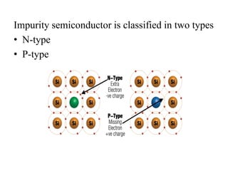
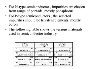
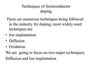
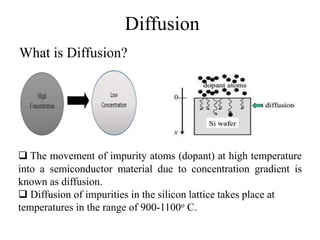
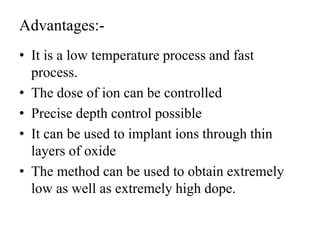
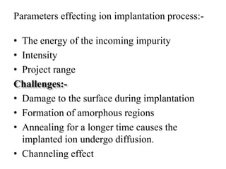
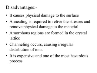
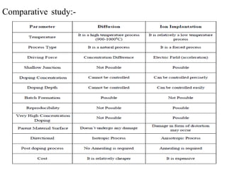
SURFACE ENGINEERING IN
ELECTRONICS INDUSTRY
SEMICONDUCTOR DOPING
Abhishek Anand
Gaole Dai
Harmeet Singh
Ishank Chopra
Yunzhe He
Introduction
• Semiconductor plays key role in the applications
in area of thermostat, IR sensors, diodes,
transistors etc.
• The gradient of concentration of a dopant in a
substrate provides different properties like
variable conductivity, light emission etc.
• Most popular material used in substrate are
silicon and germanium.
Type of semiconductors
Two kind of semiconductors:-
• Intrinsic semiconductor- Intrinsic semiconductor
is pure . It has poor electric conduction.
• Extrinsic semiconductor- Extrinsic semiconductor
is also known as impurity semiconductor.
• It is lightly or moderately doped and it has great
capacity of electric conduction.
• A semiconductor doped to high levels such as it
acts like conductor called degenerate.
Impurity semiconductor is classified in two types
• N-type
• P-type
• For N-type semiconductor , impurities are chosen
from range of pentads, mostly phosphorus
• For P-type semiconductors , the selected
impurities should be trivalent elements, mostly
boron.
• The following table shows the various materials
used in semiconductor industry
Techniques of Semiconductor
doping
There are numerous techniques being followed
in the industry for doping, most widely used
techniques are
• Ion implantation
• Diffusion
• Oxidation
We are going to focus on two major techniques;
Diffusion and Ion implantation
Diffusion
What is Diffusion?
 The movement of impurity atoms (dopant) at high temperature
into a semiconductor material due to concentration gradient is
known as diffusion.
 Diffusion of impurities in the silicon lattice takes place at
temperatures in the range of 900-1100o C.
There are two major ways in which diffusion
doping process can be carried out:
• Predeposition: The impurities diffuse into the
parent material with a constant concentration
gradient.
• Drive-in: A layer of the dopant is deposited on
the surface. In this case, the impurity gradient
at the surface of the substrate decreases with
time.
Predeposition Drive-In
Diffusion at microscopic level
Substitution diffusion
Interstitial diffusion
Diffusion process parameters
• Temperature
• Type of impurity
• Diffusion time
• Defects in silicon crystal
Challenges:-
• Crystal structure:
• Junction depth control
• Doping concentration control:
Advantages:-
• No damage to surface
• Batch fabrication is possible
• An isotropic process
• Cost associated with process is low
Disadvantages:-
• Low dose doping is difficult to carry out
• Shallow junctions are difficult to fabricate
• Cant be carried out at room temperature
Ion implantation
• What is ion implantation?
Ions of the desired dopant are first accelerated
using an electric field resulting in formation of
a beam of ions. The beam is then projected
upon the parent lattice material causing a
bombardment of the ions on the substrate
resulting in a uniform deposition of dopant on
the parent lattice.
The Process
• In order to form a beam of ions, the first step is to
generate ions.
• The dopants are heated on a hot filament causing
generation of ions.
• The ions generated are accelerated away from the
source by electric field.
• The ions then pass through a magnetic field
which diverts the ions and separates them
according to their size or according to the
requirement using a predesigned aperture.
 The separated ions are brought to the desired energy by accelerating
them again using an electric field and are bombarded on the
substrate after passing through a focusing lens.
 The focused accelerated ions strike the substrate and get implanted
in the area exposed to the beam.
Advantages:-
• It is a low temperature process and fast
process.
• The dose of ion can be controlled
• Precise depth control possible
• It can be used to implant ions through thin
layers of oxide
• The method can be used to obtain extremely
low as well as extremely high dope.
Parameters effecting ion implantation process:-
• The energy of the incoming impurity
• Intensity
• Project range
Challenges:-
• Damage to the surface during implantation
• Formation of amorphous regions
• Annealing for a longer time causes the
implanted ion undergo diffusion.
• Channeling effect
Disadvantages:-
• It causes physical damage to the surface
• Annealing is required to relive the stresses and
remove physical damage to the material
• Amorphous regions are formed in the crystal
lattice
• Channeling occurs, causing irregular
distribution of ions.
• It is expensive and one of the most hazardous
process.
Comparative study:-
Conclusion:-
• The driving force in the diffusion process is the
difference between the concentrations of the
materials involved, is carried out at high
temperature. It is a non-destructive process and
causes no damage to the material surface. Batch
formation is possible with diffusion process,
increasing the overall output
• The Ion Implantation process offers better doping
concentration control, precise junction depth
control, and easy reproducibility and doesn’t
require high temperature for being carried out.
The ion implanted product has to undergo
annealing process to repair the damage which
makes this process relatively expensive.
Feedback
• An improvement to the ion implantation process is the plasma
immersion ion implantation (PIII). In PIII process, the parent
material is directly immersed in a plasma chamber. The chamber has
plasma of ions of the impurity to be implanted. The chamber is then
impulse with a very high negative potential.
• This potential drives the electron and lead to formation of a positive
cloud around the parent material. The positive ion round the parent
material is attracted towards the material due to its negative
potential and it gets implanted on the surface uniformly.
• PIII is a non-line of sight technique unlike the conventional process
and it doesn’t require all the complexities and sophisticated
mechanisms of the conventional Ion Implantation Method.
• It is a simpler, cheaper, less time consuming, less hazardous and
flexible process than the conventional Ion Implantation.
References
1. J D Plummer, M D Deal and P B Griffin, “Silicon VLSI Technology: fundamentals,
practice and modelling”, Pearson Edu. Inc., 2001
2. Razeghi and Manijeh, “Technology of Quantum Devices”, Springer, 2010
3. Bose D.N., “Semiconductor Material and Devices”, New Age Publishers, 2012
4. F.G, Tseng, “IC Fabrication Process 2: Diffusion, Ion Implantation, Film Deposition,
Interconnection and contacts”. Lecture conducted from National Tsing Hua University,
Taiwan.
5. John (2010, June 1), “Diffusion of impurities for IC fabrication”
6. R.C. Jaeger (vol.5), Introduction to Microelectronic fabrication, Pearson Education
Inc., New Jersey,USA ,2002
7. Advancements in ion implantation Modelling for Doping of Semiconductors, Sivaco,
Inc. Available [Online] http://www.silvaco.com/content/kbase/ion_implantation.pdf
8. Plummer D. James, Deal Michael , Griffin D. Peter, “Silicon VLSI Technology:
Fundamentals, Practise and Modelling”, Prentice Hall , 2000.
9. Gupta Dushyant (2011) , “Plasma Immersion Ion Implantation Process Physics and
Technology", International Journal of Advancements in Technology.
THANK YOU
QUESTIONS?

Presentation project6

  • 1.
    SURFACE ENGINEERING IN ELECTRONICSINDUSTRY SEMICONDUCTOR DOPING Abhishek Anand Gaole Dai Harmeet Singh Ishank Chopra Yunzhe He
  • 2.
    Introduction • Semiconductor playskey role in the applications in area of thermostat, IR sensors, diodes, transistors etc. • The gradient of concentration of a dopant in a substrate provides different properties like variable conductivity, light emission etc. • Most popular material used in substrate are silicon and germanium.
  • 3.
    Type of semiconductors Twokind of semiconductors:- • Intrinsic semiconductor- Intrinsic semiconductor is pure . It has poor electric conduction. • Extrinsic semiconductor- Extrinsic semiconductor is also known as impurity semiconductor. • It is lightly or moderately doped and it has great capacity of electric conduction. • A semiconductor doped to high levels such as it acts like conductor called degenerate.
  • 4.
    Impurity semiconductor isclassified in two types • N-type • P-type
  • 5.
    • For N-typesemiconductor , impurities are chosen from range of pentads, mostly phosphorus • For P-type semiconductors , the selected impurities should be trivalent elements, mostly boron. • The following table shows the various materials used in semiconductor industry
  • 6.
    Techniques of Semiconductor doping Thereare numerous techniques being followed in the industry for doping, most widely used techniques are • Ion implantation • Diffusion • Oxidation We are going to focus on two major techniques; Diffusion and Ion implantation
  • 7.
    Diffusion What is Diffusion? The movement of impurity atoms (dopant) at high temperature into a semiconductor material due to concentration gradient is known as diffusion.  Diffusion of impurities in the silicon lattice takes place at temperatures in the range of 900-1100o C.
  • 8.
    There are twomajor ways in which diffusion doping process can be carried out: • Predeposition: The impurities diffuse into the parent material with a constant concentration gradient. • Drive-in: A layer of the dopant is deposited on the surface. In this case, the impurity gradient at the surface of the substrate decreases with time. Predeposition Drive-In
  • 9.
    Diffusion at microscopiclevel Substitution diffusion Interstitial diffusion
  • 10.
    Diffusion process parameters •Temperature • Type of impurity • Diffusion time • Defects in silicon crystal Challenges:- • Crystal structure: • Junction depth control • Doping concentration control:
  • 11.
    Advantages:- • No damageto surface • Batch fabrication is possible • An isotropic process • Cost associated with process is low Disadvantages:- • Low dose doping is difficult to carry out • Shallow junctions are difficult to fabricate • Cant be carried out at room temperature
  • 12.
    Ion implantation • Whatis ion implantation? Ions of the desired dopant are first accelerated using an electric field resulting in formation of a beam of ions. The beam is then projected upon the parent lattice material causing a bombardment of the ions on the substrate resulting in a uniform deposition of dopant on the parent lattice.
  • 13.
    The Process • Inorder to form a beam of ions, the first step is to generate ions. • The dopants are heated on a hot filament causing generation of ions. • The ions generated are accelerated away from the source by electric field. • The ions then pass through a magnetic field which diverts the ions and separates them according to their size or according to the requirement using a predesigned aperture.
  • 14.
     The separatedions are brought to the desired energy by accelerating them again using an electric field and are bombarded on the substrate after passing through a focusing lens.  The focused accelerated ions strike the substrate and get implanted in the area exposed to the beam.
  • 15.
    Advantages:- • It isa low temperature process and fast process. • The dose of ion can be controlled • Precise depth control possible • It can be used to implant ions through thin layers of oxide • The method can be used to obtain extremely low as well as extremely high dope.
  • 16.
    Parameters effecting ionimplantation process:- • The energy of the incoming impurity • Intensity • Project range Challenges:- • Damage to the surface during implantation • Formation of amorphous regions • Annealing for a longer time causes the implanted ion undergo diffusion. • Channeling effect
  • 17.
    Disadvantages:- • It causesphysical damage to the surface • Annealing is required to relive the stresses and remove physical damage to the material • Amorphous regions are formed in the crystal lattice • Channeling occurs, causing irregular distribution of ions. • It is expensive and one of the most hazardous process.
  • 18.
  • 19.
    Conclusion:- • The drivingforce in the diffusion process is the difference between the concentrations of the materials involved, is carried out at high temperature. It is a non-destructive process and causes no damage to the material surface. Batch formation is possible with diffusion process, increasing the overall output • The Ion Implantation process offers better doping concentration control, precise junction depth control, and easy reproducibility and doesn’t require high temperature for being carried out. The ion implanted product has to undergo annealing process to repair the damage which makes this process relatively expensive.
  • 20.
    Feedback • An improvementto the ion implantation process is the plasma immersion ion implantation (PIII). In PIII process, the parent material is directly immersed in a plasma chamber. The chamber has plasma of ions of the impurity to be implanted. The chamber is then impulse with a very high negative potential. • This potential drives the electron and lead to formation of a positive cloud around the parent material. The positive ion round the parent material is attracted towards the material due to its negative potential and it gets implanted on the surface uniformly. • PIII is a non-line of sight technique unlike the conventional process and it doesn’t require all the complexities and sophisticated mechanisms of the conventional Ion Implantation Method. • It is a simpler, cheaper, less time consuming, less hazardous and flexible process than the conventional Ion Implantation.
  • 21.
    References 1. J DPlummer, M D Deal and P B Griffin, “Silicon VLSI Technology: fundamentals, practice and modelling”, Pearson Edu. Inc., 2001 2. Razeghi and Manijeh, “Technology of Quantum Devices”, Springer, 2010 3. Bose D.N., “Semiconductor Material and Devices”, New Age Publishers, 2012 4. F.G, Tseng, “IC Fabrication Process 2: Diffusion, Ion Implantation, Film Deposition, Interconnection and contacts”. Lecture conducted from National Tsing Hua University, Taiwan. 5. John (2010, June 1), “Diffusion of impurities for IC fabrication” 6. R.C. Jaeger (vol.5), Introduction to Microelectronic fabrication, Pearson Education Inc., New Jersey,USA ,2002 7. Advancements in ion implantation Modelling for Doping of Semiconductors, Sivaco, Inc. Available [Online] http://www.silvaco.com/content/kbase/ion_implantation.pdf 8. Plummer D. James, Deal Michael , Griffin D. Peter, “Silicon VLSI Technology: Fundamentals, Practise and Modelling”, Prentice Hall , 2000. 9. Gupta Dushyant (2011) , “Plasma Immersion Ion Implantation Process Physics and Technology", International Journal of Advancements in Technology.
  • 22.