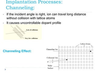
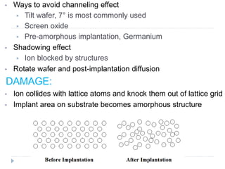
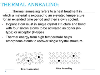
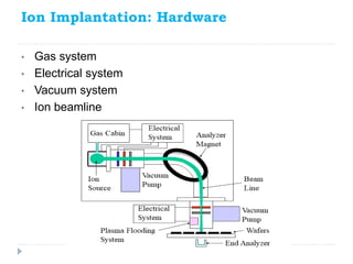
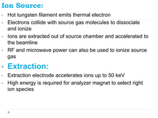
SlideShare a Scribd company logo
Ion implantation
KIRUBAKARAN
20304011
PONDICHERRY UNIVERSITY
Ion implantation:
Ion implantation is a low-temperature
process by which ions of one element are
accelerated into a solid target, thereby changing the
physical, chemical, or electrical properties of the
target. Ion implantation is used in semiconductor
device fabrication and in metal finishing, as well as
in materials science research.
Ion Implantation Control:
 Beam current and implantation time control dopant
concentration
 Ion energy controls junction depth
 Dopant profile is anisotropic
Stopping Mechanism:
 Ions penetrate into substrate
 Collide with lattice atoms
 Gradually lose their energy and stop
 Two stop mechanisms
Two Stopping Mechanism:
 Nuclear stopping
 Collision with nuclei of the lattice atoms
 Scattered significantly
 Causes crystal structure damage.
 electronic stopping
 Collision with electrons of the lattice atoms
 Incident ion path is almost unchanged
 Energy transfer is very small
 Crystal structure damage is negligible
Implantation Processes:
Channeling:
• If the incident angle is right, ion can travel long distance
without collision with lattice atoms
• It causes uncontrollable dopant profile
Channeling Effect:
• Ways to avoid channeling effect
 Tilt wafer, 7° is most commonly used
 Screen oxide
 Pre-amorphous implantation, Germanium
• Shadowing effect
 Ion blocked by structures
• Rotate wafer and post-implantation diffusion
DAMAGE:
• Ion collides with lattice atoms and knock them out of lattice grid
• Implant area on substrate becomes amorphous structure
THERMAL ANNEALING:
Thermal annealing refers to a heat treatment in
which a material is exposed to an elevated temperature
for an extended time period and then slowly cooled.
• Dopant atom must in single crystal structure and bond
with four silicon atoms to be activated as donor (N-
type) or acceptor (P-type)
• Thermal energy from high temperature helps
amorphous atoms to recover single crystal structure.
Ion Implantation: Hardware
• Gas system
• Electrical system
• Vacuum system
• Ion beamline
 Gas System:
• Special gas deliver system to handle hazardous gases
• Special training needed to change gases bottles
• Argon is used for purge and beam calibration
 Electrical System:
• High voltage system
– Determine ion energy that controls junction depth
• High voltage system
– Determine ion energy that controls junction depth
• RF system
– Some ion sources use RF to generate ions
Vacuum System:
• Need high vacuum to accelerate ions and reduce collision
• MFP >> beamline length
• 10-5 to 10-7 Torr
• Turbo pump and Cryo pump
• Exhaust system
• Control System:
• Ion energy, beam current, and ion species.
• Mechanical parts for loading and unloading
• Wafer movement to get uniform beam scan
• CPU board control boards
– Control boards collect data from the systems, send
it to CPU board to process,
– CPU sends instructions back to the systems
through the control board
Ion Source:
• Hot tungsten filament emits thermal electron
• Electrons collide with source gas molecules to dissociate
and ionize
• Ions are extracted out of source chamber and accelerated to
the beamline
• RF and microwave power can also be used to ionize source
gas
• Extraction:
• Extraction electrode accelerates ions up to 50 keV
• High energy is required for analyzer magnet to select right
ion species
Analyzer Magnet:
• Gyro radius of charge particle in magnetic field relate with B-
field and mass/charge ratio
• Used for isotope separation to get enriched U235
• Only ions with right mass/charge ratio can go through the
slit
• Purified the implanting ion beam
Safety:
One of most hazardous process tools in semiconductor
industry
• Chemical
• Electro-magnetic
• Mechanical
Chemical Safety:
Most dopant materials are highly toxic, flammable and explosive.
• Poisonous and explosive: AsH3 , PH3 , B2H6
• Corrosive: BF3
• Toxic: P, B, As, Sb
Electro-magnetic Safety:
High voltage: from facility 208 V to acceleration electrode up to
50 kV.
• Ground strip
• Lock & tag
• Magnetic field: pacemaker, etc
Radiation Safety:
• High energy ions cause strong X-ray
radiation
• Normally well shield.
Mechanical Safety:
Moving parts, doors, valves and robots
• Spin wheel
ADVANTAGE:
 Precise control of dose, depth profile and area
uniformity.
 Excellent reproducibility.
 Wide choice of masks.
 Low temperature process.
 Small lateral spread of dopants.
 Vacuum cleanliness.
DISADVANTAGE:
 Expensive & complicated equipment.
 Very deep and very shallow profiles are difficult.
 Not all the damage can be corrected by annealing.
 Typically has higher impurity content than does
diffusion.
 Often uses extremely toxic gas sources such as
arsine (AsH3), and phosphine (PH3).

More Related Content

What's hot

Ion beam lithography
Ion beam lithographyIon beam lithography
Ion beam lithography
Hoang Tien
 
Photolithography and its procedure
Photolithography and its procedurePhotolithography and its procedure
Photolithography and its procedure
karoline Enoch
 
Extreme ultraviolet lithography ppt
Extreme ultraviolet lithography pptExtreme ultraviolet lithography ppt
Extreme ultraviolet lithography ppt
sumang89
 

What's hot (20)

Optical properties of nanoparticles
Optical properties of nanoparticlesOptical properties of nanoparticles
Optical properties of nanoparticles
 
laser ablation and pyrolysis for micro machining and nano fabrication
laser ablation and pyrolysis for micro machining and nano fabricationlaser ablation and pyrolysis for micro machining and nano fabrication
laser ablation and pyrolysis for micro machining and nano fabrication
 
ZnS Nanostructures: Synthesis, Characterization, and Theory - Defense Present...
ZnS Nanostructures: Synthesis, Characterization, and Theory - Defense Present...ZnS Nanostructures: Synthesis, Characterization, and Theory - Defense Present...
ZnS Nanostructures: Synthesis, Characterization, and Theory - Defense Present...
 
Ion beam lithography
Ion beam lithographyIon beam lithography
Ion beam lithography
 
PVD,CVD,AFM.ppt
PVD,CVD,AFM.pptPVD,CVD,AFM.ppt
PVD,CVD,AFM.ppt
 
organic solar cell
organic solar cellorganic solar cell
organic solar cell
 
mems and nems
mems and nemsmems and nems
mems and nems
 
Preparation of thin films
Preparation of thin filmsPreparation of thin films
Preparation of thin films
 
Sputtering process and its types
Sputtering process and its typesSputtering process and its types
Sputtering process and its types
 
vlsi annealing and masking
vlsi annealing and maskingvlsi annealing and masking
vlsi annealing and masking
 
Plasma Etching
Plasma Etching Plasma Etching
Plasma Etching
 
Vapour Solid Liquid Growth
Vapour Solid Liquid GrowthVapour Solid Liquid Growth
Vapour Solid Liquid Growth
 
Arc discharge method
Arc discharge methodArc discharge method
Arc discharge method
 
Chemical Vapour Deposition
Chemical Vapour DepositionChemical Vapour Deposition
Chemical Vapour Deposition
 
Ion Implantation UPS.pdf
Ion Implantation UPS.pdfIon Implantation UPS.pdf
Ion Implantation UPS.pdf
 
Photolithography and its procedure
Photolithography and its procedurePhotolithography and its procedure
Photolithography and its procedure
 
Silicon Manufacturing
Silicon ManufacturingSilicon Manufacturing
Silicon Manufacturing
 
Semiconductor Nanomaterials
Semiconductor NanomaterialsSemiconductor Nanomaterials
Semiconductor Nanomaterials
 
Thin film deposition using spray pyrolysis
Thin film deposition using spray pyrolysisThin film deposition using spray pyrolysis
Thin film deposition using spray pyrolysis
 
Extreme ultraviolet lithography ppt
Extreme ultraviolet lithography pptExtreme ultraviolet lithography ppt
Extreme ultraviolet lithography ppt
 

Similar to Ion implantation

Similar to Ion implantation (20)

Mass spectrometry
Mass spectrometryMass spectrometry
Mass spectrometry
 
Radiopharmaceutical
Radiopharmaceutical Radiopharmaceutical
Radiopharmaceutical
 
Mohd wahid (aes)
Mohd wahid (aes)Mohd wahid (aes)
Mohd wahid (aes)
 
Pelletron and van de graff generator
Pelletron and van de graff generatorPelletron and van de graff generator
Pelletron and van de graff generator
 
ICP AES overview-Nipa 25.01.2023.pptx
ICP AES overview-Nipa 25.01.2023.pptxICP AES overview-Nipa 25.01.2023.pptx
ICP AES overview-Nipa 25.01.2023.pptx
 
Atomic absorption spectrophotometry
Atomic absorption spectrophotometryAtomic absorption spectrophotometry
Atomic absorption spectrophotometry
 
Mass spectrometry
Mass spectrometryMass spectrometry
Mass spectrometry
 
IONIMPLANTATION (1).pptx
IONIMPLANTATION (1).pptxIONIMPLANTATION (1).pptx
IONIMPLANTATION (1).pptx
 
05-BAT-Mass-Spec-Heena-1.pdf
05-BAT-Mass-Spec-Heena-1.pdf05-BAT-Mass-Spec-Heena-1.pdf
05-BAT-Mass-Spec-Heena-1.pdf
 
ION IMPLANTATION
ION IMPLANTATIONION IMPLANTATION
ION IMPLANTATION
 
MASS SPECTROSCOPY.pptx by Pranav Lendhey
MASS SPECTROSCOPY.pptx by Pranav LendheyMASS SPECTROSCOPY.pptx by Pranav Lendhey
MASS SPECTROSCOPY.pptx by Pranav Lendhey
 
Mass spectrometry
Mass spectrometryMass spectrometry
Mass spectrometry
 
Principles of Medical Cyclotrons and Applications.pptx
Principles of Medical Cyclotrons and Applications.pptxPrinciples of Medical Cyclotrons and Applications.pptx
Principles of Medical Cyclotrons and Applications.pptx
 
GREEN ENERGY
GREEN ENERGYGREEN ENERGY
GREEN ENERGY
 
EEG - Montages, Equipment and Basic Physics
EEG - Montages, Equipment and Basic PhysicsEEG - Montages, Equipment and Basic Physics
EEG - Montages, Equipment and Basic Physics
 
Uv,vis,nmr,mass,ir
Uv,vis,nmr,mass,irUv,vis,nmr,mass,ir
Uv,vis,nmr,mass,ir
 
Ion beam etching (or) Ion milling
Ion beam etching (or) Ion millingIon beam etching (or) Ion milling
Ion beam etching (or) Ion milling
 
Introduction of mass spectrometer - basic types of mass analyzer
Introduction of mass spectrometer - basic types of mass analyzer Introduction of mass spectrometer - basic types of mass analyzer
Introduction of mass spectrometer - basic types of mass analyzer
 
Photodetector (Photodiode)
Photodetector (Photodiode)Photodetector (Photodiode)
Photodetector (Photodiode)
 
A Seminar on Nuclear Battery
A Seminar on Nuclear BatteryA Seminar on Nuclear Battery
A Seminar on Nuclear Battery
 

Recently uploaded

RS Khurmi Machine Design Clutch and Brake Exercise Numerical Solutions
RS Khurmi Machine Design Clutch and Brake Exercise Numerical SolutionsRS Khurmi Machine Design Clutch and Brake Exercise Numerical Solutions
RS Khurmi Machine Design Clutch and Brake Exercise Numerical Solutions
Atif Razi
 
CFD Simulation of By-pass Flow in a HRSG module by R&R Consult.pptx
CFD Simulation of By-pass Flow in a HRSG module by R&R Consult.pptxCFD Simulation of By-pass Flow in a HRSG module by R&R Consult.pptx
CFD Simulation of By-pass Flow in a HRSG module by R&R Consult.pptx
R&R Consult
 
power quality voltage fluctuation UNIT - I.pptx
power quality voltage fluctuation UNIT - I.pptxpower quality voltage fluctuation UNIT - I.pptx
power quality voltage fluctuation UNIT - I.pptx
ViniHema
 
Digital Signal Processing Lecture notes n.pdf
Digital Signal Processing Lecture notes n.pdfDigital Signal Processing Lecture notes n.pdf
Digital Signal Processing Lecture notes n.pdf
AbrahamGadissa
 
Hall booking system project report .pdf
Hall booking system project report  .pdfHall booking system project report  .pdf
Hall booking system project report .pdf
Kamal Acharya
 

Recently uploaded (20)

A case study of cinema management system project report..pdf
A case study of cinema management system project report..pdfA case study of cinema management system project report..pdf
A case study of cinema management system project report..pdf
 
The Ultimate Guide to External Floating Roofs for Oil Storage Tanks.docx
The Ultimate Guide to External Floating Roofs for Oil Storage Tanks.docxThe Ultimate Guide to External Floating Roofs for Oil Storage Tanks.docx
The Ultimate Guide to External Floating Roofs for Oil Storage Tanks.docx
 
İTÜ CAD and Reverse Engineering Workshop
İTÜ CAD and Reverse Engineering WorkshopİTÜ CAD and Reverse Engineering Workshop
İTÜ CAD and Reverse Engineering Workshop
 
WATER CRISIS and its solutions-pptx 1234
WATER CRISIS and its solutions-pptx 1234WATER CRISIS and its solutions-pptx 1234
WATER CRISIS and its solutions-pptx 1234
 
Danfoss NeoCharge Technology -A Revolution in 2024.pdf
Danfoss NeoCharge Technology -A Revolution in 2024.pdfDanfoss NeoCharge Technology -A Revolution in 2024.pdf
Danfoss NeoCharge Technology -A Revolution in 2024.pdf
 
Construction method of steel structure space frame .pptx
Construction method of steel structure space frame .pptxConstruction method of steel structure space frame .pptx
Construction method of steel structure space frame .pptx
 
RS Khurmi Machine Design Clutch and Brake Exercise Numerical Solutions
RS Khurmi Machine Design Clutch and Brake Exercise Numerical SolutionsRS Khurmi Machine Design Clutch and Brake Exercise Numerical Solutions
RS Khurmi Machine Design Clutch and Brake Exercise Numerical Solutions
 
NO1 Pandit Amil Baba In Bahawalpur, Sargodha, Sialkot, Sheikhupura, Rahim Yar...
NO1 Pandit Amil Baba In Bahawalpur, Sargodha, Sialkot, Sheikhupura, Rahim Yar...NO1 Pandit Amil Baba In Bahawalpur, Sargodha, Sialkot, Sheikhupura, Rahim Yar...
NO1 Pandit Amil Baba In Bahawalpur, Sargodha, Sialkot, Sheikhupura, Rahim Yar...
 
Sachpazis:Terzaghi Bearing Capacity Estimation in simple terms with Calculati...
Sachpazis:Terzaghi Bearing Capacity Estimation in simple terms with Calculati...Sachpazis:Terzaghi Bearing Capacity Estimation in simple terms with Calculati...
Sachpazis:Terzaghi Bearing Capacity Estimation in simple terms with Calculati...
 
Scaling in conventional MOSFET for constant electric field and constant voltage
Scaling in conventional MOSFET for constant electric field and constant voltageScaling in conventional MOSFET for constant electric field and constant voltage
Scaling in conventional MOSFET for constant electric field and constant voltage
 
shape functions of 1D and 2 D rectangular elements.pptx
shape functions of 1D and 2 D rectangular elements.pptxshape functions of 1D and 2 D rectangular elements.pptx
shape functions of 1D and 2 D rectangular elements.pptx
 
Quality defects in TMT Bars, Possible causes and Potential Solutions.
Quality defects in TMT Bars, Possible causes and Potential Solutions.Quality defects in TMT Bars, Possible causes and Potential Solutions.
Quality defects in TMT Bars, Possible causes and Potential Solutions.
 
Introduction to Casting Processes in Manufacturing
Introduction to Casting Processes in ManufacturingIntroduction to Casting Processes in Manufacturing
Introduction to Casting Processes in Manufacturing
 
CFD Simulation of By-pass Flow in a HRSG module by R&R Consult.pptx
CFD Simulation of By-pass Flow in a HRSG module by R&R Consult.pptxCFD Simulation of By-pass Flow in a HRSG module by R&R Consult.pptx
CFD Simulation of By-pass Flow in a HRSG module by R&R Consult.pptx
 
power quality voltage fluctuation UNIT - I.pptx
power quality voltage fluctuation UNIT - I.pptxpower quality voltage fluctuation UNIT - I.pptx
power quality voltage fluctuation UNIT - I.pptx
 
Digital Signal Processing Lecture notes n.pdf
Digital Signal Processing Lecture notes n.pdfDigital Signal Processing Lecture notes n.pdf
Digital Signal Processing Lecture notes n.pdf
 
weather web application report.pdf
weather web application report.pdfweather web application report.pdf
weather web application report.pdf
 
Final project report on grocery store management system..pdf
Final project report on grocery store management system..pdfFinal project report on grocery store management system..pdf
Final project report on grocery store management system..pdf
 
Hall booking system project report .pdf
Hall booking system project report  .pdfHall booking system project report  .pdf
Hall booking system project report .pdf
 
Top 13 Famous Civil Engineering Scientist
Top 13 Famous Civil Engineering ScientistTop 13 Famous Civil Engineering Scientist
Top 13 Famous Civil Engineering Scientist
 

Ion implantation

  • 2. Ion implantation: Ion implantation is a low-temperature process by which ions of one element are accelerated into a solid target, thereby changing the physical, chemical, or electrical properties of the target. Ion implantation is used in semiconductor device fabrication and in metal finishing, as well as in materials science research. Ion Implantation Control:  Beam current and implantation time control dopant concentration  Ion energy controls junction depth  Dopant profile is anisotropic
  • 3. Stopping Mechanism:  Ions penetrate into substrate  Collide with lattice atoms  Gradually lose their energy and stop  Two stop mechanisms Two Stopping Mechanism:  Nuclear stopping  Collision with nuclei of the lattice atoms  Scattered significantly  Causes crystal structure damage.  electronic stopping  Collision with electrons of the lattice atoms  Incident ion path is almost unchanged  Energy transfer is very small  Crystal structure damage is negligible
  • 4. Implantation Processes: Channeling: • If the incident angle is right, ion can travel long distance without collision with lattice atoms • It causes uncontrollable dopant profile Channeling Effect:
  • 5. • Ways to avoid channeling effect  Tilt wafer, 7° is most commonly used  Screen oxide  Pre-amorphous implantation, Germanium • Shadowing effect  Ion blocked by structures • Rotate wafer and post-implantation diffusion DAMAGE: • Ion collides with lattice atoms and knock them out of lattice grid • Implant area on substrate becomes amorphous structure
  • 6. THERMAL ANNEALING: Thermal annealing refers to a heat treatment in which a material is exposed to an elevated temperature for an extended time period and then slowly cooled. • Dopant atom must in single crystal structure and bond with four silicon atoms to be activated as donor (N- type) or acceptor (P-type) • Thermal energy from high temperature helps amorphous atoms to recover single crystal structure.
  • 7. Ion Implantation: Hardware • Gas system • Electrical system • Vacuum system • Ion beamline
  • 8.  Gas System: • Special gas deliver system to handle hazardous gases • Special training needed to change gases bottles • Argon is used for purge and beam calibration  Electrical System: • High voltage system – Determine ion energy that controls junction depth • High voltage system – Determine ion energy that controls junction depth • RF system – Some ion sources use RF to generate ions Vacuum System: • Need high vacuum to accelerate ions and reduce collision • MFP >> beamline length • 10-5 to 10-7 Torr
  • 9. • Turbo pump and Cryo pump • Exhaust system • Control System: • Ion energy, beam current, and ion species. • Mechanical parts for loading and unloading • Wafer movement to get uniform beam scan • CPU board control boards – Control boards collect data from the systems, send it to CPU board to process, – CPU sends instructions back to the systems through the control board
  • 10. Ion Source: • Hot tungsten filament emits thermal electron • Electrons collide with source gas molecules to dissociate and ionize • Ions are extracted out of source chamber and accelerated to the beamline • RF and microwave power can also be used to ionize source gas • Extraction: • Extraction electrode accelerates ions up to 50 keV • High energy is required for analyzer magnet to select right ion species
  • 11. Analyzer Magnet: • Gyro radius of charge particle in magnetic field relate with B- field and mass/charge ratio • Used for isotope separation to get enriched U235 • Only ions with right mass/charge ratio can go through the slit • Purified the implanting ion beam
  • 12. Safety: One of most hazardous process tools in semiconductor industry • Chemical • Electro-magnetic • Mechanical Chemical Safety: Most dopant materials are highly toxic, flammable and explosive. • Poisonous and explosive: AsH3 , PH3 , B2H6 • Corrosive: BF3 • Toxic: P, B, As, Sb
  • 13. Electro-magnetic Safety: High voltage: from facility 208 V to acceleration electrode up to 50 kV. • Ground strip • Lock & tag • Magnetic field: pacemaker, etc Radiation Safety: • High energy ions cause strong X-ray radiation • Normally well shield. Mechanical Safety: Moving parts, doors, valves and robots • Spin wheel
  • 14. ADVANTAGE:  Precise control of dose, depth profile and area uniformity.  Excellent reproducibility.  Wide choice of masks.  Low temperature process.  Small lateral spread of dopants.  Vacuum cleanliness.
  • 15. DISADVANTAGE:  Expensive & complicated equipment.  Very deep and very shallow profiles are difficult.  Not all the damage can be corrected by annealing.  Typically has higher impurity content than does diffusion.  Often uses extremely toxic gas sources such as arsine (AsH3), and phosphine (PH3).