Downloaded 202 times


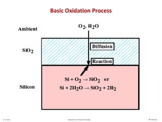


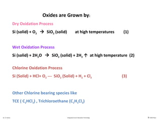

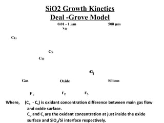


Thermal oxidation is a process used to grow silicon dioxide films on silicon substrates. It involves heating silicon in an oxygen-containing environment to form a stable silicon-dioxide layer. The growth rate of the oxide layer follows a Deal-Grove model based on diffusion and reaction kinetics. While this model accurately describes thicker oxide growth, additional terms are needed to model the initially faster growth rate of very thin oxides. The oxidation rate depends on factors like temperature, oxidizing ambient, crystal orientation, and dopant concentration.


