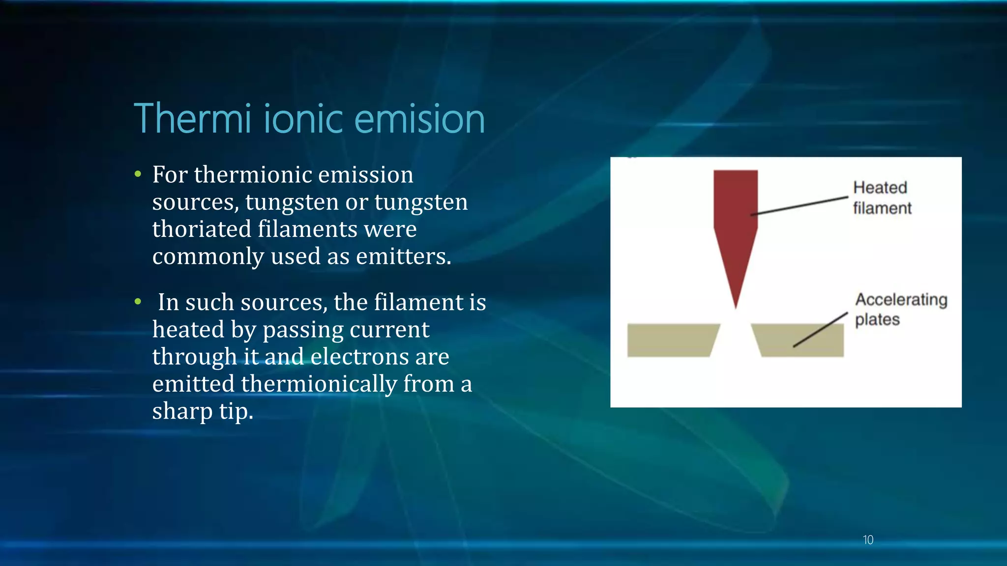
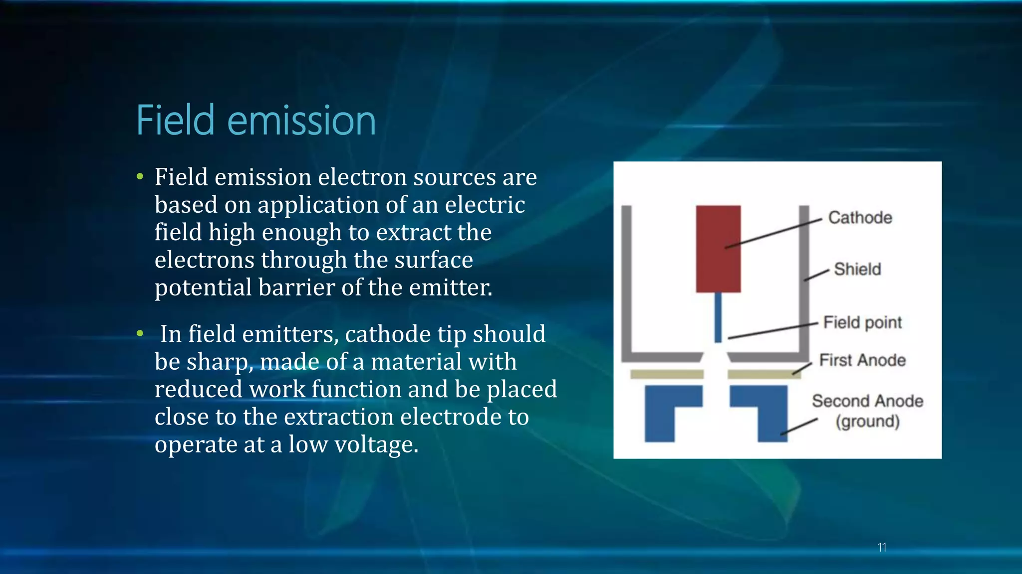
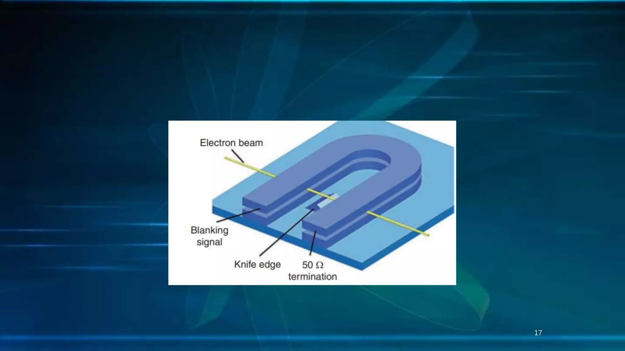
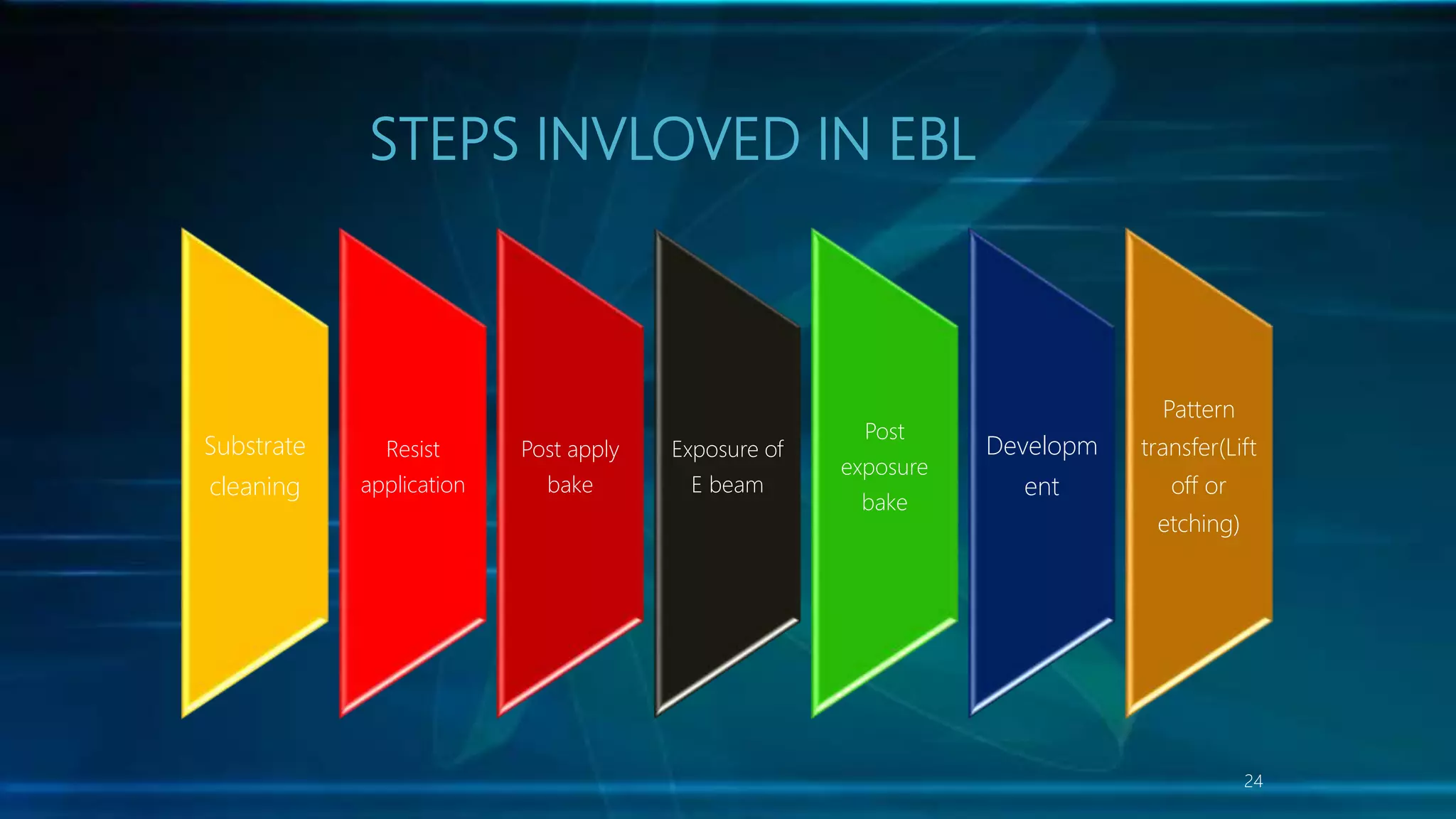
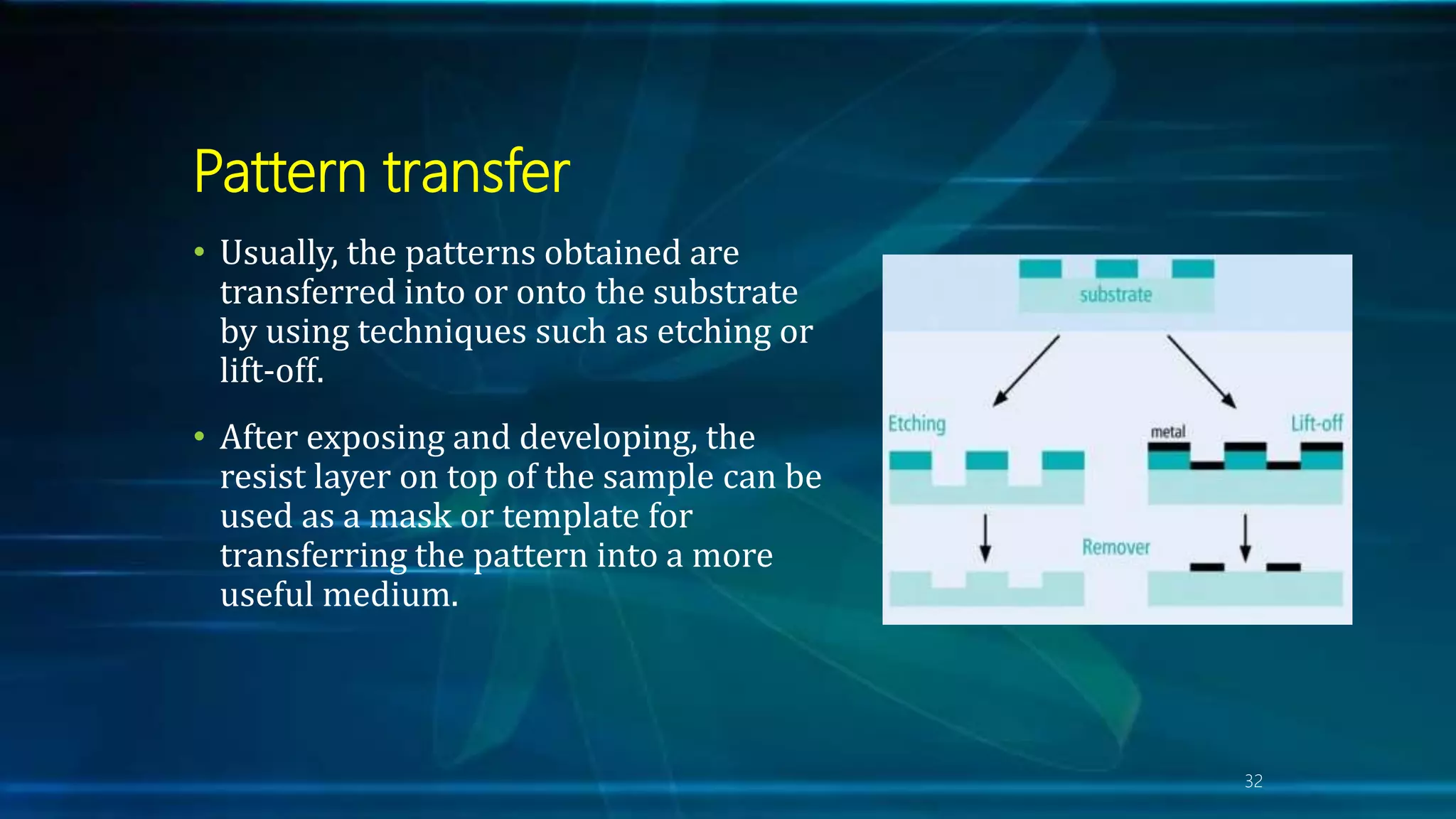
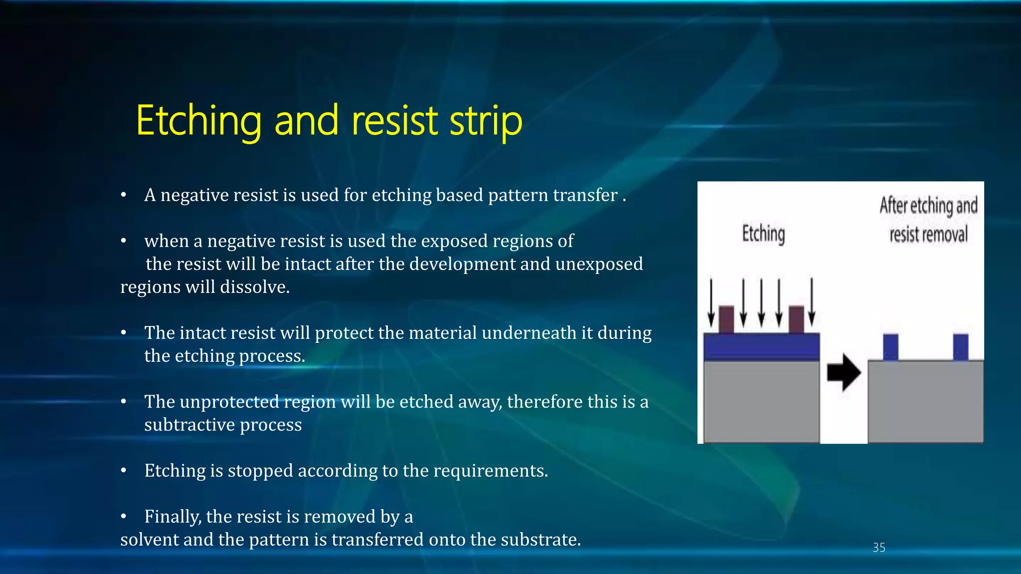
Electron beam lithography (e-beam lithography) is a high-resolution patterning technique that employs a focused electron beam to expose a resist layer on a substrate, allowing for the creation of features as small as a few nanometers. It provides superior resolution compared to traditional optical lithography but has lower throughput, making it suitable for small-area, low-volume applications or photomask production. The process involves steps such as substrate cleaning, resist application, exposure, development, and pattern transfer, with applications in nanostructured devices and various electronic components.