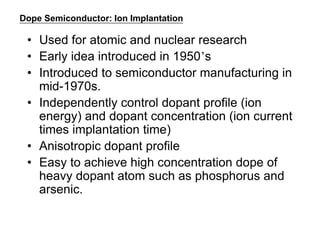
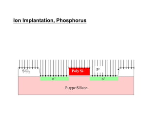
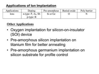
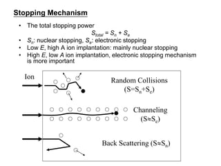
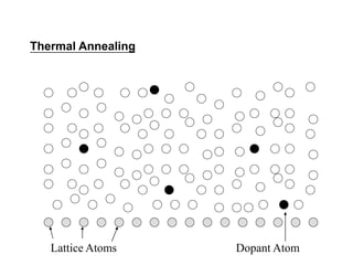
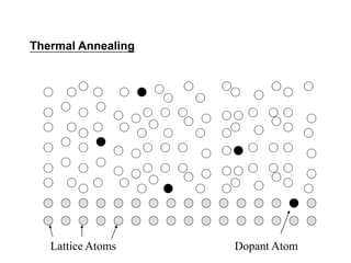
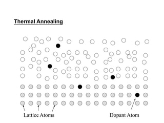
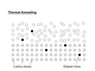
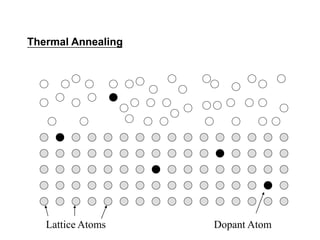
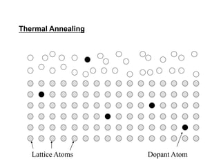
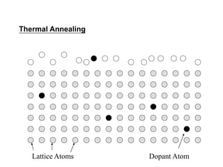
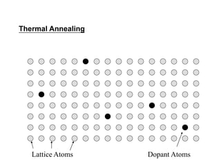
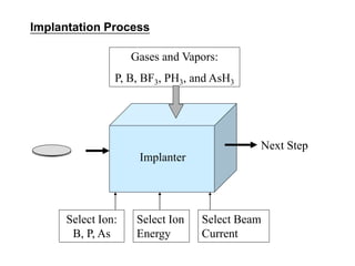
SlideShare a Scribd company logo
1 of 46
Ion Implantation
Materials
Design
Masks
IC Fab
Test
Packaging
Final Test
Thermal
Processes
Photo-
lithography
Etch
PR strip
Implant
PR strip
Metalization CMP
Dielectric
deposition
Wafers
Wafer Process Flow
Introduction: Dope Semiconductor
• What is Semiconductor?
• Why semiconductor need to be doped?
• What is n-type dopant?
• What is p-type dopant?
• Dope semiconductor
– Two way to dope
• Diffusion
• Ion implantation
• Other application of ion implantation
Dopant Oxide Deposition
Si Substrate
SiO2
Deposited Dopant Oxide
Oxidation
Si Substrate
SiO2
Drive-in
Si Substrate
SiO2
Doped junction
Strip and Clean
Si Substrate
SiO2
Doped junction
Dope Semiconductor: Ion Implantation
• Used for atomic and nuclear research
• Early idea introduced in 1950’s
• Introduced to semiconductor manufacturing in
mid-1970s.
• Independently control dopant profile (ion
energy) and dopant concentration (ion current
times implantation time)
• Anisotropic dopant profile
• Easy to achieve high concentration dope of
heavy dopant atom such as phosphorus and
arsenic.
Ion Implantation, Phosphorus
Poly Si
n+
P-type Silicon
n+
SiO2
P+
Comparison of
Implantation and Diffusion
PRSiO2
Si Si
Ion implantationDiffusion
Doped region
Junction depth
Comparison of Implantation and Diffusion
Diffusion Ion Implantation
High temperature, hard mask Low temperature, photoresist mask
Isotropic dopant profile Anisotropic dopant profile
Cannot independently control of the dopant
concentration and junction depth
Can independently control of the dopant
concentration and junction depth
Batch process Both Batch and single wafer process
Applications of Ion Implantation
Applications Doping Pre-amorphous Buried oxide Poly barrier
Ions n-type: P, As, Sb
p-type: B
Si or Ge O N
Other Applications
• Oxygen implantation for silicon-on-insulator
(SOI) device
• Pre-amorphous silicon implantation on
titanium film for better annealing
• Pre-amorphous germanium implantation on
silicon substrate for profile control
Stopping Mechanism
• Ions penetrate into substrate
• Collide with lattice atoms
• Gradually lose their energy and stop
• Two stop mechanisms
– Nuclear stopping
• Collision with nuclei of the lattice atoms
• Scattered significantly
• Causes crystal structure damage.
– electronic stopping
• Collision with electrons of the lattice atoms
• Incident ion path is almost unchanged
• Energy transfer is very small
• Crystal structure damage is negligible
Stopping Mechanism
• The total stopping power
Stotal = Sn + Se
• Sn: nuclear stopping, Se: electronic stopping
• Low E, high A ion implantation: mainly nuclear stopping
• High E, low A ion implantation, electronic stopping mechanism
is more important
Random Collisions
(S=Sn+Se)
Channeling
(SSe)
Back Scattering (SSn)
Ion
Stopping Power and Ion Velocity
Nuclear
Stopping
Electronic
Stopping
I II III
Ion Velocity
StoppingPower
Implantation Processes: Channeling
• If the incident angle is right, ion can travel long
distance without collision with lattice atoms
• It causes uncontrollable dopant profile
Very few collisions
Lots of collisions
Channeling Effect
Channeling Ion
Collisional Ion
Lattice Atoms
q
Wafer
Surface
Post-collision Channeling
Implantation Processes: Channeling
• Ways to avoid channeling effect
– Tilt wafer, 7° is most commonly used
– Pre-amorphous implantation, Germanium
• Shadowing effect
– Ion blocked by structures
• Rotate wafer and post-implantation diffusion
Question
• Why don’t people use channeling effect
to create deep junction without high ion
energy?
Answer:
– Ion beam is not perfectly parallel. Many
ions will start to have a lot of nuclear
collisions with lattice atoms after they
penetrating into the substrate. Some ions
can channel deep into the substrate, while
many others are stopped as the normal
Gaussian distribution.
Damage Process
• Implanted ions transfer energy to lattice
atoms
– Atoms to break free
• Freed atoms collide with other lattice
atoms
– Free more lattice atoms
– Damage continues until all freed atoms
stop
• One energetic ion can cause thousands
of displacements of lattice atoms
Lattice Damage With One Ion
Heavy Ion
Single Crystal Silicon
Damaged Region
Light Ion
Implantation Processes: Damage
• Ion collides with lattice atoms and knock
them out of lattice grid
• Implant area on substrate becomes
amorphous structure
Before Implantation After Implantation
Implantation Processes: Anneal
• Dopant atom must in single crystal
structure and bond with four silicon
atoms to be activated as donor (N-type)
or acceptor (P-type)
• Thermal energy from high temperature
helps amorphous atoms to recover
single crystal structure.
Thermal Annealing
Dopant AtomLattice Atoms
Thermal Annealing
Dopant AtomLattice Atoms
Thermal Annealing
Dopant AtomLattice Atoms
Thermal Annealing
Dopant AtomLattice Atoms
Thermal Annealing
Dopant AtomLattice Atoms
Thermal Annealing
Dopant AtomLattice Atoms
Thermal Annealing
Dopant AtomLattice Atoms
Thermal Annealing
Dopant AtomsLattice Atoms
Implantation Processes: Annealing
Before Annealing After Annealing
Rapid Thermal Annealing (RTA)
• At high temperature, annealing out pace
diffusion
• Rapid thermal process (RTP) is widely
used for post-implantation anneal
• RTA is fast (less than a minute), better
WTW (With in Wafer) uniformity, and
minimized the dopant diffusion
Ion Implantation: Hardware
• Gas system
• Electrical system
• Vacuum system
• Ion beamline
Implantation Process
Gases and Vapors:
P, B, BF3, PH3, and AsH3
Select Ion:
B, P, As
Select Ion
Energy
Select Beam
Current
Next Step
Implanter
Ion Implanter
Gas Cabin
Ion
Source
Vacuum
Pump
Vacuum
Pump
Electrical
System
Electrical
System
Analyzer
Magnet
Beam
Line
End Analyzer
WafersPlasma Flooding
System
Ion Implantation
• Gas System
– Special gas deliver system
to handle hazardous
gases
– Special training needed to
change gases bottles
– Argon is used for beam
calibration
• Electrical System
– High voltage system
• Determine ion energy
that controls junction
depth
– RF system
• Some ion sources use
RF to generate ions
• Vacuum System
– Need high vacuum to accelerate ions and
reduce collision
– MFP >> beamline length
– 10-5 to 10-7 Torr
– Turbo pump and Cryo pump
– Exhaust system
• Control System
– Ion energy, beam current, and ion
species.
– Mechanical parts for loading and
unloading
– Wafer movement to get uniform beam
scan
– CPU board control boards
• Control boards collect data from the
systems, send it to CPU board to
process,
• CPU sends instructions back to the
systems through the control board.
Ion Implantation: Beamline
• Ion source
• Extraction electrode
• Analyzer magnet
• Post acceleration
• Plasma flooding system
• End analyzer
Ion implanter: Ion Source
• Hot tungsten filament emits thermal electron
• Electrons collide with source gas molecules to dissociate and ionize
• Ions are extracted out of source chamber and accelerated to the beamline
• RF and microwave power can also be used to ionize source gas
Ion Implantation: Extraction
• Extraction electrode accelerates ions up to 50 keV
• High energy is required for analyzer magnet to select
right ion species.
Charge Neutralization System
• Implanted ions charge wafer positively
• Cause wafer charging effect
• Expel positive ion, cause beam blowup and result non-uniform
dopant distribution
• Discharge arcing create defects on wafer
• Breakdown gate oxide, low yield
• Need eliminate or minimize charging effect
Charge Neutralization System
• Need to provide electrons to neutralize ions
• Plasma flooding system
• Electron gun
• Electron shower are used to
Ion Implantation: Plasma Flooding System
• Ions cause wafer charging
• Wafer charging can cause non-uniform doping and arcing defects
• Elections are “flooding” into ion beam and neutralized the charge on
the wafer
• Argon plasma generated by thermal electrons emit from hot tungsten
filament
Wafer Handling
• Ion beam diameter: ~25 mm (~1”),
• Wafer diameter: 200 mm (8”) or larger
• Needs to move beam or wafer, or both, to scan ion beam across the
whole wafer
– Spin wheel
– Spin disk
– Single wafer scan

More Related Content

What's hot

Metal semiconductor contacts
Metal semiconductor contactsMetal semiconductor contacts
Metal semiconductor contactsKasif Nabi
 
Ion Implantation UPS.pdf
Ion Implantation UPS.pdfIon Implantation UPS.pdf
Ion Implantation UPS.pdfssuser0e2fb9
 
Metallization
Metallization Metallization
Metallization GKGanesh2
 
Ic technology-pattern transfer and etching
Ic technology-pattern transfer and etchingIc technology-pattern transfer and etching
Ic technology-pattern transfer and etchingkriticka sharma
 
Metal Oxide Semiconductor Fet (Mosfet)
Metal Oxide Semiconductor Fet (Mosfet)Metal Oxide Semiconductor Fet (Mosfet)
Metal Oxide Semiconductor Fet (Mosfet)stooty s
 
Fully depleted silicon insulator
Fully depleted silicon insulatorFully depleted silicon insulator
Fully depleted silicon insulatorsandeep sandy
 
PHOTODETECTORS
PHOTODETECTORSPHOTODETECTORS
PHOTODETECTORSAakankshaR
 
Lithography, Photolithography--ABU SYED KUET
Lithography, Photolithography--ABU SYED KUETLithography, Photolithography--ABU SYED KUET
Lithography, Photolithography--ABU SYED KUETA. S. M. Jannatul Islam
 
VLSI Design(Fabrication)
VLSI Design(Fabrication)VLSI Design(Fabrication)
VLSI Design(Fabrication)Trijit Mallick
 
Silicon on Insulator (SOI) Technology
Silicon on Insulator (SOI) TechnologySilicon on Insulator (SOI) Technology
Silicon on Insulator (SOI) TechnologySudhanshu Janwadkar
 
Photodetector (Photodiode)
Photodetector (Photodiode)Photodetector (Photodiode)
Photodetector (Photodiode)Kalyan Acharjya
 

What's hot (20)

Metal semiconductor contacts
Metal semiconductor contactsMetal semiconductor contacts
Metal semiconductor contacts
 
Ion Implantation UPS.pdf
Ion Implantation UPS.pdfIon Implantation UPS.pdf
Ion Implantation UPS.pdf
 
Etching
EtchingEtching
Etching
 
Cmos fabrication
Cmos fabricationCmos fabrication
Cmos fabrication
 
Metallization
Metallization Metallization
Metallization
 
Ic technology-pattern transfer and etching
Ic technology-pattern transfer and etchingIc technology-pattern transfer and etching
Ic technology-pattern transfer and etching
 
Fabrication of P-N Junction
Fabrication of P-N JunctionFabrication of P-N Junction
Fabrication of P-N Junction
 
Plasma Etching
Plasma Etching Plasma Etching
Plasma Etching
 
Metal Oxide Semiconductor Fet (Mosfet)
Metal Oxide Semiconductor Fet (Mosfet)Metal Oxide Semiconductor Fet (Mosfet)
Metal Oxide Semiconductor Fet (Mosfet)
 
Epitaxy growth
Epitaxy growthEpitaxy growth
Epitaxy growth
 
Fully depleted silicon insulator
Fully depleted silicon insulatorFully depleted silicon insulator
Fully depleted silicon insulator
 
wet etching
wet etchingwet etching
wet etching
 
Device isolation Techniques
Device isolation TechniquesDevice isolation Techniques
Device isolation Techniques
 
PHOTODETECTORS
PHOTODETECTORSPHOTODETECTORS
PHOTODETECTORS
 
Lithography, Photolithography--ABU SYED KUET
Lithography, Photolithography--ABU SYED KUETLithography, Photolithography--ABU SYED KUET
Lithography, Photolithography--ABU SYED KUET
 
Cmos
CmosCmos
Cmos
 
MOSFET fabrication 12
MOSFET fabrication 12MOSFET fabrication 12
MOSFET fabrication 12
 
VLSI Design(Fabrication)
VLSI Design(Fabrication)VLSI Design(Fabrication)
VLSI Design(Fabrication)
 
Silicon on Insulator (SOI) Technology
Silicon on Insulator (SOI) TechnologySilicon on Insulator (SOI) Technology
Silicon on Insulator (SOI) Technology
 
Photodetector (Photodiode)
Photodetector (Photodiode)Photodetector (Photodiode)
Photodetector (Photodiode)
 

Similar to Ion implantation VLSI

Nanomaterial Synthesis Method
Nanomaterial Synthesis MethodNanomaterial Synthesis Method
Nanomaterial Synthesis MethodTanvir Moin
 
Ion beam etching (or) Ion milling
Ion beam etching (or) Ion millingIon beam etching (or) Ion milling
Ion beam etching (or) Ion millingBoda Omkareshwar
 
IONIMPLANTATION (1).pptx
IONIMPLANTATION (1).pptxIONIMPLANTATION (1).pptx
IONIMPLANTATION (1).pptxTOUFEEQPTAJE
 
Lecture 2 ic fabrication processing & wafer preparation
Lecture 2 ic fabrication processing & wafer preparationLecture 2 ic fabrication processing & wafer preparation
Lecture 2 ic fabrication processing & wafer preparationDr. Ghanshyam Singh
 
Micro plasma fet (mopfet) [autosaved]
Micro plasma fet (mopfet) [autosaved]Micro plasma fet (mopfet) [autosaved]
Micro plasma fet (mopfet) [autosaved]Nitisha S
 
Sarah aull secondary electron yield of srf materials
Sarah aull   secondary electron yield of srf materialsSarah aull   secondary electron yield of srf materials
Sarah aull secondary electron yield of srf materialsthinfilmsworkshop
 
Sarah aull secondary electron yield of srf materials
Sarah aull   secondary electron yield of srf materialsSarah aull   secondary electron yield of srf materials
Sarah aull secondary electron yield of srf materialsthinfilmsworkshop
 
Plasma 4th types of matter.ppt
Plasma 4th types of matter.pptPlasma 4th types of matter.ppt
Plasma 4th types of matter.pptHubaioos
 
2012 tus lecture 7
2012 tus lecture 72012 tus lecture 7
2012 tus lecture 7AllenHermann
 
esp operation SIPAT.ppt
esp operation SIPAT.pptesp operation SIPAT.ppt
esp operation SIPAT.pptKhemantOd
 
Research presentation slideshare
Research presentation slideshareResearch presentation slideshare
Research presentation slideshareTakeru Arai
 
Vacuum Science and Technology for Thin Film Device Processing
Vacuum Science and Technology for Thin Film Device ProcessingVacuum Science and Technology for Thin Film Device Processing
Vacuum Science and Technology for Thin Film Device Processingcdtpv
 
An introduction to radiation effect on electronic devices
An introduction to radiation effect on electronic devicesAn introduction to radiation effect on electronic devices
An introduction to radiation effect on electronic devicesFrancesco Poderico
 
High speed semiconductor devices ppt
High speed semiconductor devices pptHigh speed semiconductor devices ppt
High speed semiconductor devices pptBalajiG107
 
Day 1 MSMS theory.ppt
Day 1 MSMS theory.pptDay 1 MSMS theory.ppt
Day 1 MSMS theory.pptemymamdoh
 

Similar to Ion implantation VLSI (20)

Ion implantation
Ion implantationIon implantation
Ion implantation
 
Nanomaterial Synthesis Method
Nanomaterial Synthesis MethodNanomaterial Synthesis Method
Nanomaterial Synthesis Method
 
Ion beam etching (or) Ion milling
Ion beam etching (or) Ion millingIon beam etching (or) Ion milling
Ion beam etching (or) Ion milling
 
IONIMPLANTATION (1).pptx
IONIMPLANTATION (1).pptxIONIMPLANTATION (1).pptx
IONIMPLANTATION (1).pptx
 
PVD.ppt
PVD.pptPVD.ppt
PVD.ppt
 
ect 292 nanoelectronics
ect 292  nanoelectronicsect 292  nanoelectronics
ect 292 nanoelectronics
 
Lecture 2 ic fabrication processing & wafer preparation
Lecture 2 ic fabrication processing & wafer preparationLecture 2 ic fabrication processing & wafer preparation
Lecture 2 ic fabrication processing & wafer preparation
 
Micro plasma fet (mopfet) [autosaved]
Micro plasma fet (mopfet) [autosaved]Micro plasma fet (mopfet) [autosaved]
Micro plasma fet (mopfet) [autosaved]
 
Final Project Plasma
Final Project PlasmaFinal Project Plasma
Final Project Plasma
 
Sarah aull secondary electron yield of srf materials
Sarah aull   secondary electron yield of srf materialsSarah aull   secondary electron yield of srf materials
Sarah aull secondary electron yield of srf materials
 
Sarah aull secondary electron yield of srf materials
Sarah aull   secondary electron yield of srf materialsSarah aull   secondary electron yield of srf materials
Sarah aull secondary electron yield of srf materials
 
Vlsi ppt priyanka
Vlsi ppt priyankaVlsi ppt priyanka
Vlsi ppt priyanka
 
Plasma 4th types of matter.ppt
Plasma 4th types of matter.pptPlasma 4th types of matter.ppt
Plasma 4th types of matter.ppt
 
2012 tus lecture 7
2012 tus lecture 72012 tus lecture 7
2012 tus lecture 7
 
esp operation SIPAT.ppt
esp operation SIPAT.pptesp operation SIPAT.ppt
esp operation SIPAT.ppt
 
Research presentation slideshare
Research presentation slideshareResearch presentation slideshare
Research presentation slideshare
 
Vacuum Science and Technology for Thin Film Device Processing
Vacuum Science and Technology for Thin Film Device ProcessingVacuum Science and Technology for Thin Film Device Processing
Vacuum Science and Technology for Thin Film Device Processing
 
An introduction to radiation effect on electronic devices
An introduction to radiation effect on electronic devicesAn introduction to radiation effect on electronic devices
An introduction to radiation effect on electronic devices
 
High speed semiconductor devices ppt
High speed semiconductor devices pptHigh speed semiconductor devices ppt
High speed semiconductor devices ppt
 
Day 1 MSMS theory.ppt
Day 1 MSMS theory.pptDay 1 MSMS theory.ppt
Day 1 MSMS theory.ppt
 

Recently uploaded

Introduction to Multiple Access Protocol.pptx
Introduction to Multiple Access Protocol.pptxIntroduction to Multiple Access Protocol.pptx
Introduction to Multiple Access Protocol.pptxupamatechverse
 
College Call Girls Nashik Nehal 7001305949 Independent Escort Service Nashik
College Call Girls Nashik Nehal 7001305949 Independent Escort Service NashikCollege Call Girls Nashik Nehal 7001305949 Independent Escort Service Nashik
College Call Girls Nashik Nehal 7001305949 Independent Escort Service NashikCall Girls in Nagpur High Profile
 
(ANVI) Koregaon Park Call Girls Just Call 7001035870 [ Cash on Delivery ] Pun...
(ANVI) Koregaon Park Call Girls Just Call 7001035870 [ Cash on Delivery ] Pun...(ANVI) Koregaon Park Call Girls Just Call 7001035870 [ Cash on Delivery ] Pun...
(ANVI) Koregaon Park Call Girls Just Call 7001035870 [ Cash on Delivery ] Pun...ranjana rawat
 
GDSC ASEB Gen AI study jams presentation
GDSC ASEB Gen AI study jams presentationGDSC ASEB Gen AI study jams presentation
GDSC ASEB Gen AI study jams presentationGDSCAESB
 
(ANJALI) Dange Chowk Call Girls Just Call 7001035870 [ Cash on Delivery ] Pun...
(ANJALI) Dange Chowk Call Girls Just Call 7001035870 [ Cash on Delivery ] Pun...(ANJALI) Dange Chowk Call Girls Just Call 7001035870 [ Cash on Delivery ] Pun...
(ANJALI) Dange Chowk Call Girls Just Call 7001035870 [ Cash on Delivery ] Pun...ranjana rawat
 
(SHREYA) Chakan Call Girls Just Call 7001035870 [ Cash on Delivery ] Pune Esc...
(SHREYA) Chakan Call Girls Just Call 7001035870 [ Cash on Delivery ] Pune Esc...(SHREYA) Chakan Call Girls Just Call 7001035870 [ Cash on Delivery ] Pune Esc...
(SHREYA) Chakan Call Girls Just Call 7001035870 [ Cash on Delivery ] Pune Esc...ranjana rawat
 
HARMONY IN THE NATURE AND EXISTENCE - Unit-IV
HARMONY IN THE NATURE AND EXISTENCE - Unit-IVHARMONY IN THE NATURE AND EXISTENCE - Unit-IV
HARMONY IN THE NATURE AND EXISTENCE - Unit-IVRajaP95
 
Sheet Pile Wall Design and Construction: A Practical Guide for Civil Engineer...
Sheet Pile Wall Design and Construction: A Practical Guide for Civil Engineer...Sheet Pile Wall Design and Construction: A Practical Guide for Civil Engineer...
Sheet Pile Wall Design and Construction: A Practical Guide for Civil Engineer...Dr.Costas Sachpazis
 
The Most Attractive Pune Call Girls Budhwar Peth 8250192130 Will You Miss Thi...
The Most Attractive Pune Call Girls Budhwar Peth 8250192130 Will You Miss Thi...The Most Attractive Pune Call Girls Budhwar Peth 8250192130 Will You Miss Thi...
The Most Attractive Pune Call Girls Budhwar Peth 8250192130 Will You Miss Thi...ranjana rawat
 
Processing & Properties of Floor and Wall Tiles.pptx
Processing & Properties of Floor and Wall Tiles.pptxProcessing & Properties of Floor and Wall Tiles.pptx
Processing & Properties of Floor and Wall Tiles.pptxpranjaldaimarysona
 
Coefficient of Thermal Expansion and their Importance.pptx
Coefficient of Thermal Expansion and their Importance.pptxCoefficient of Thermal Expansion and their Importance.pptx
Coefficient of Thermal Expansion and their Importance.pptxAsutosh Ranjan
 
VIP Call Girls Service Kondapur Hyderabad Call +91-8250192130
VIP Call Girls Service Kondapur Hyderabad Call +91-8250192130VIP Call Girls Service Kondapur Hyderabad Call +91-8250192130
VIP Call Girls Service Kondapur Hyderabad Call +91-8250192130Suhani Kapoor
 
High Profile Call Girls Nagpur Isha Call 7001035870 Meet With Nagpur Escorts
High Profile Call Girls Nagpur Isha Call 7001035870 Meet With Nagpur EscortsHigh Profile Call Girls Nagpur Isha Call 7001035870 Meet With Nagpur Escorts
High Profile Call Girls Nagpur Isha Call 7001035870 Meet With Nagpur Escortsranjana rawat
 
Porous Ceramics seminar and technical writing
Porous Ceramics seminar and technical writingPorous Ceramics seminar and technical writing
Porous Ceramics seminar and technical writingrakeshbaidya232001
 
Call Girls in Nagpur Suman Call 7001035870 Meet With Nagpur Escorts
Call Girls in Nagpur Suman Call 7001035870 Meet With Nagpur EscortsCall Girls in Nagpur Suman Call 7001035870 Meet With Nagpur Escorts
Call Girls in Nagpur Suman Call 7001035870 Meet With Nagpur EscortsCall Girls in Nagpur High Profile
 
Analog to Digital and Digital to Analog Converter
Analog to Digital and Digital to Analog ConverterAnalog to Digital and Digital to Analog Converter
Analog to Digital and Digital to Analog ConverterAbhinavSharma374939
 
What are the advantages and disadvantages of membrane structures.pptx
What are the advantages and disadvantages of membrane structures.pptxWhat are the advantages and disadvantages of membrane structures.pptx
What are the advantages and disadvantages of membrane structures.pptxwendy cai
 
Decoding Kotlin - Your guide to solving the mysterious in Kotlin.pptx
Decoding Kotlin - Your guide to solving the mysterious in Kotlin.pptxDecoding Kotlin - Your guide to solving the mysterious in Kotlin.pptx
Decoding Kotlin - Your guide to solving the mysterious in Kotlin.pptxJoão Esperancinha
 

Recently uploaded (20)

Introduction to Multiple Access Protocol.pptx
Introduction to Multiple Access Protocol.pptxIntroduction to Multiple Access Protocol.pptx
Introduction to Multiple Access Protocol.pptx
 
College Call Girls Nashik Nehal 7001305949 Independent Escort Service Nashik
College Call Girls Nashik Nehal 7001305949 Independent Escort Service NashikCollege Call Girls Nashik Nehal 7001305949 Independent Escort Service Nashik
College Call Girls Nashik Nehal 7001305949 Independent Escort Service Nashik
 
(ANVI) Koregaon Park Call Girls Just Call 7001035870 [ Cash on Delivery ] Pun...
(ANVI) Koregaon Park Call Girls Just Call 7001035870 [ Cash on Delivery ] Pun...(ANVI) Koregaon Park Call Girls Just Call 7001035870 [ Cash on Delivery ] Pun...
(ANVI) Koregaon Park Call Girls Just Call 7001035870 [ Cash on Delivery ] Pun...
 
GDSC ASEB Gen AI study jams presentation
GDSC ASEB Gen AI study jams presentationGDSC ASEB Gen AI study jams presentation
GDSC ASEB Gen AI study jams presentation
 
(ANJALI) Dange Chowk Call Girls Just Call 7001035870 [ Cash on Delivery ] Pun...
(ANJALI) Dange Chowk Call Girls Just Call 7001035870 [ Cash on Delivery ] Pun...(ANJALI) Dange Chowk Call Girls Just Call 7001035870 [ Cash on Delivery ] Pun...
(ANJALI) Dange Chowk Call Girls Just Call 7001035870 [ Cash on Delivery ] Pun...
 
(SHREYA) Chakan Call Girls Just Call 7001035870 [ Cash on Delivery ] Pune Esc...
(SHREYA) Chakan Call Girls Just Call 7001035870 [ Cash on Delivery ] Pune Esc...(SHREYA) Chakan Call Girls Just Call 7001035870 [ Cash on Delivery ] Pune Esc...
(SHREYA) Chakan Call Girls Just Call 7001035870 [ Cash on Delivery ] Pune Esc...
 
HARMONY IN THE NATURE AND EXISTENCE - Unit-IV
HARMONY IN THE NATURE AND EXISTENCE - Unit-IVHARMONY IN THE NATURE AND EXISTENCE - Unit-IV
HARMONY IN THE NATURE AND EXISTENCE - Unit-IV
 
Sheet Pile Wall Design and Construction: A Practical Guide for Civil Engineer...
Sheet Pile Wall Design and Construction: A Practical Guide for Civil Engineer...Sheet Pile Wall Design and Construction: A Practical Guide for Civil Engineer...
Sheet Pile Wall Design and Construction: A Practical Guide for Civil Engineer...
 
★ CALL US 9953330565 ( HOT Young Call Girls In Badarpur delhi NCR
★ CALL US 9953330565 ( HOT Young Call Girls In Badarpur delhi NCR★ CALL US 9953330565 ( HOT Young Call Girls In Badarpur delhi NCR
★ CALL US 9953330565 ( HOT Young Call Girls In Badarpur delhi NCR
 
The Most Attractive Pune Call Girls Budhwar Peth 8250192130 Will You Miss Thi...
The Most Attractive Pune Call Girls Budhwar Peth 8250192130 Will You Miss Thi...The Most Attractive Pune Call Girls Budhwar Peth 8250192130 Will You Miss Thi...
The Most Attractive Pune Call Girls Budhwar Peth 8250192130 Will You Miss Thi...
 
Processing & Properties of Floor and Wall Tiles.pptx
Processing & Properties of Floor and Wall Tiles.pptxProcessing & Properties of Floor and Wall Tiles.pptx
Processing & Properties of Floor and Wall Tiles.pptx
 
Coefficient of Thermal Expansion and their Importance.pptx
Coefficient of Thermal Expansion and their Importance.pptxCoefficient of Thermal Expansion and their Importance.pptx
Coefficient of Thermal Expansion and their Importance.pptx
 
VIP Call Girls Service Kondapur Hyderabad Call +91-8250192130
VIP Call Girls Service Kondapur Hyderabad Call +91-8250192130VIP Call Girls Service Kondapur Hyderabad Call +91-8250192130
VIP Call Girls Service Kondapur Hyderabad Call +91-8250192130
 
High Profile Call Girls Nagpur Isha Call 7001035870 Meet With Nagpur Escorts
High Profile Call Girls Nagpur Isha Call 7001035870 Meet With Nagpur EscortsHigh Profile Call Girls Nagpur Isha Call 7001035870 Meet With Nagpur Escorts
High Profile Call Girls Nagpur Isha Call 7001035870 Meet With Nagpur Escorts
 
Porous Ceramics seminar and technical writing
Porous Ceramics seminar and technical writingPorous Ceramics seminar and technical writing
Porous Ceramics seminar and technical writing
 
Call Girls in Nagpur Suman Call 7001035870 Meet With Nagpur Escorts
Call Girls in Nagpur Suman Call 7001035870 Meet With Nagpur EscortsCall Girls in Nagpur Suman Call 7001035870 Meet With Nagpur Escorts
Call Girls in Nagpur Suman Call 7001035870 Meet With Nagpur Escorts
 
Exploring_Network_Security_with_JA3_by_Rakesh Seal.pptx
Exploring_Network_Security_with_JA3_by_Rakesh Seal.pptxExploring_Network_Security_with_JA3_by_Rakesh Seal.pptx
Exploring_Network_Security_with_JA3_by_Rakesh Seal.pptx
 
Analog to Digital and Digital to Analog Converter
Analog to Digital and Digital to Analog ConverterAnalog to Digital and Digital to Analog Converter
Analog to Digital and Digital to Analog Converter
 
What are the advantages and disadvantages of membrane structures.pptx
What are the advantages and disadvantages of membrane structures.pptxWhat are the advantages and disadvantages of membrane structures.pptx
What are the advantages and disadvantages of membrane structures.pptx
 
Decoding Kotlin - Your guide to solving the mysterious in Kotlin.pptx
Decoding Kotlin - Your guide to solving the mysterious in Kotlin.pptxDecoding Kotlin - Your guide to solving the mysterious in Kotlin.pptx
Decoding Kotlin - Your guide to solving the mysterious in Kotlin.pptx
 

Ion implantation VLSI

  • 2. Materials Design Masks IC Fab Test Packaging Final Test Thermal Processes Photo- lithography Etch PR strip Implant PR strip Metalization CMP Dielectric deposition Wafers Wafer Process Flow
  • 3. Introduction: Dope Semiconductor • What is Semiconductor? • Why semiconductor need to be doped? • What is n-type dopant? • What is p-type dopant? • Dope semiconductor – Two way to dope • Diffusion • Ion implantation • Other application of ion implantation
  • 4. Dopant Oxide Deposition Si Substrate SiO2 Deposited Dopant Oxide
  • 7. Strip and Clean Si Substrate SiO2 Doped junction
  • 8. Dope Semiconductor: Ion Implantation • Used for atomic and nuclear research • Early idea introduced in 1950’s • Introduced to semiconductor manufacturing in mid-1970s. • Independently control dopant profile (ion energy) and dopant concentration (ion current times implantation time) • Anisotropic dopant profile • Easy to achieve high concentration dope of heavy dopant atom such as phosphorus and arsenic.
  • 9. Ion Implantation, Phosphorus Poly Si n+ P-type Silicon n+ SiO2 P+
  • 10. Comparison of Implantation and Diffusion PRSiO2 Si Si Ion implantationDiffusion Doped region Junction depth
  • 11. Comparison of Implantation and Diffusion Diffusion Ion Implantation High temperature, hard mask Low temperature, photoresist mask Isotropic dopant profile Anisotropic dopant profile Cannot independently control of the dopant concentration and junction depth Can independently control of the dopant concentration and junction depth Batch process Both Batch and single wafer process
  • 12. Applications of Ion Implantation Applications Doping Pre-amorphous Buried oxide Poly barrier Ions n-type: P, As, Sb p-type: B Si or Ge O N Other Applications • Oxygen implantation for silicon-on-insulator (SOI) device • Pre-amorphous silicon implantation on titanium film for better annealing • Pre-amorphous germanium implantation on silicon substrate for profile control
  • 13. Stopping Mechanism • Ions penetrate into substrate • Collide with lattice atoms • Gradually lose their energy and stop • Two stop mechanisms – Nuclear stopping • Collision with nuclei of the lattice atoms • Scattered significantly • Causes crystal structure damage. – electronic stopping • Collision with electrons of the lattice atoms • Incident ion path is almost unchanged • Energy transfer is very small • Crystal structure damage is negligible
  • 14. Stopping Mechanism • The total stopping power Stotal = Sn + Se • Sn: nuclear stopping, Se: electronic stopping • Low E, high A ion implantation: mainly nuclear stopping • High E, low A ion implantation, electronic stopping mechanism is more important Random Collisions (S=Sn+Se) Channeling (SSe) Back Scattering (SSn) Ion
  • 15. Stopping Power and Ion Velocity Nuclear Stopping Electronic Stopping I II III Ion Velocity StoppingPower
  • 16. Implantation Processes: Channeling • If the incident angle is right, ion can travel long distance without collision with lattice atoms • It causes uncontrollable dopant profile Very few collisions Lots of collisions
  • 17. Channeling Effect Channeling Ion Collisional Ion Lattice Atoms q Wafer Surface
  • 19. Implantation Processes: Channeling • Ways to avoid channeling effect – Tilt wafer, 7° is most commonly used – Pre-amorphous implantation, Germanium • Shadowing effect – Ion blocked by structures • Rotate wafer and post-implantation diffusion
  • 20. Question • Why don’t people use channeling effect to create deep junction without high ion energy?
  • 21. Answer: – Ion beam is not perfectly parallel. Many ions will start to have a lot of nuclear collisions with lattice atoms after they penetrating into the substrate. Some ions can channel deep into the substrate, while many others are stopped as the normal Gaussian distribution.
  • 22. Damage Process • Implanted ions transfer energy to lattice atoms – Atoms to break free • Freed atoms collide with other lattice atoms – Free more lattice atoms – Damage continues until all freed atoms stop • One energetic ion can cause thousands of displacements of lattice atoms
  • 23. Lattice Damage With One Ion Heavy Ion Single Crystal Silicon Damaged Region Light Ion
  • 24. Implantation Processes: Damage • Ion collides with lattice atoms and knock them out of lattice grid • Implant area on substrate becomes amorphous structure Before Implantation After Implantation
  • 25. Implantation Processes: Anneal • Dopant atom must in single crystal structure and bond with four silicon atoms to be activated as donor (N-type) or acceptor (P-type) • Thermal energy from high temperature helps amorphous atoms to recover single crystal structure.
  • 34. Implantation Processes: Annealing Before Annealing After Annealing
  • 35. Rapid Thermal Annealing (RTA) • At high temperature, annealing out pace diffusion • Rapid thermal process (RTP) is widely used for post-implantation anneal • RTA is fast (less than a minute), better WTW (With in Wafer) uniformity, and minimized the dopant diffusion
  • 36. Ion Implantation: Hardware • Gas system • Electrical system • Vacuum system • Ion beamline
  • 37. Implantation Process Gases and Vapors: P, B, BF3, PH3, and AsH3 Select Ion: B, P, As Select Ion Energy Select Beam Current Next Step Implanter
  • 39. Ion Implantation • Gas System – Special gas deliver system to handle hazardous gases – Special training needed to change gases bottles – Argon is used for beam calibration • Electrical System – High voltage system • Determine ion energy that controls junction depth – RF system • Some ion sources use RF to generate ions • Vacuum System – Need high vacuum to accelerate ions and reduce collision – MFP >> beamline length – 10-5 to 10-7 Torr – Turbo pump and Cryo pump – Exhaust system • Control System – Ion energy, beam current, and ion species. – Mechanical parts for loading and unloading – Wafer movement to get uniform beam scan – CPU board control boards • Control boards collect data from the systems, send it to CPU board to process, • CPU sends instructions back to the systems through the control board.
  • 40. Ion Implantation: Beamline • Ion source • Extraction electrode • Analyzer magnet • Post acceleration • Plasma flooding system • End analyzer
  • 41. Ion implanter: Ion Source • Hot tungsten filament emits thermal electron • Electrons collide with source gas molecules to dissociate and ionize • Ions are extracted out of source chamber and accelerated to the beamline • RF and microwave power can also be used to ionize source gas
  • 42. Ion Implantation: Extraction • Extraction electrode accelerates ions up to 50 keV • High energy is required for analyzer magnet to select right ion species.
  • 43. Charge Neutralization System • Implanted ions charge wafer positively • Cause wafer charging effect • Expel positive ion, cause beam blowup and result non-uniform dopant distribution • Discharge arcing create defects on wafer • Breakdown gate oxide, low yield • Need eliminate or minimize charging effect
  • 44. Charge Neutralization System • Need to provide electrons to neutralize ions • Plasma flooding system • Electron gun • Electron shower are used to
  • 45. Ion Implantation: Plasma Flooding System • Ions cause wafer charging • Wafer charging can cause non-uniform doping and arcing defects • Elections are “flooding” into ion beam and neutralized the charge on the wafer • Argon plasma generated by thermal electrons emit from hot tungsten filament
  • 46. Wafer Handling • Ion beam diameter: ~25 mm (~1”), • Wafer diameter: 200 mm (8”) or larger • Needs to move beam or wafer, or both, to scan ion beam across the whole wafer – Spin wheel – Spin disk – Single wafer scan