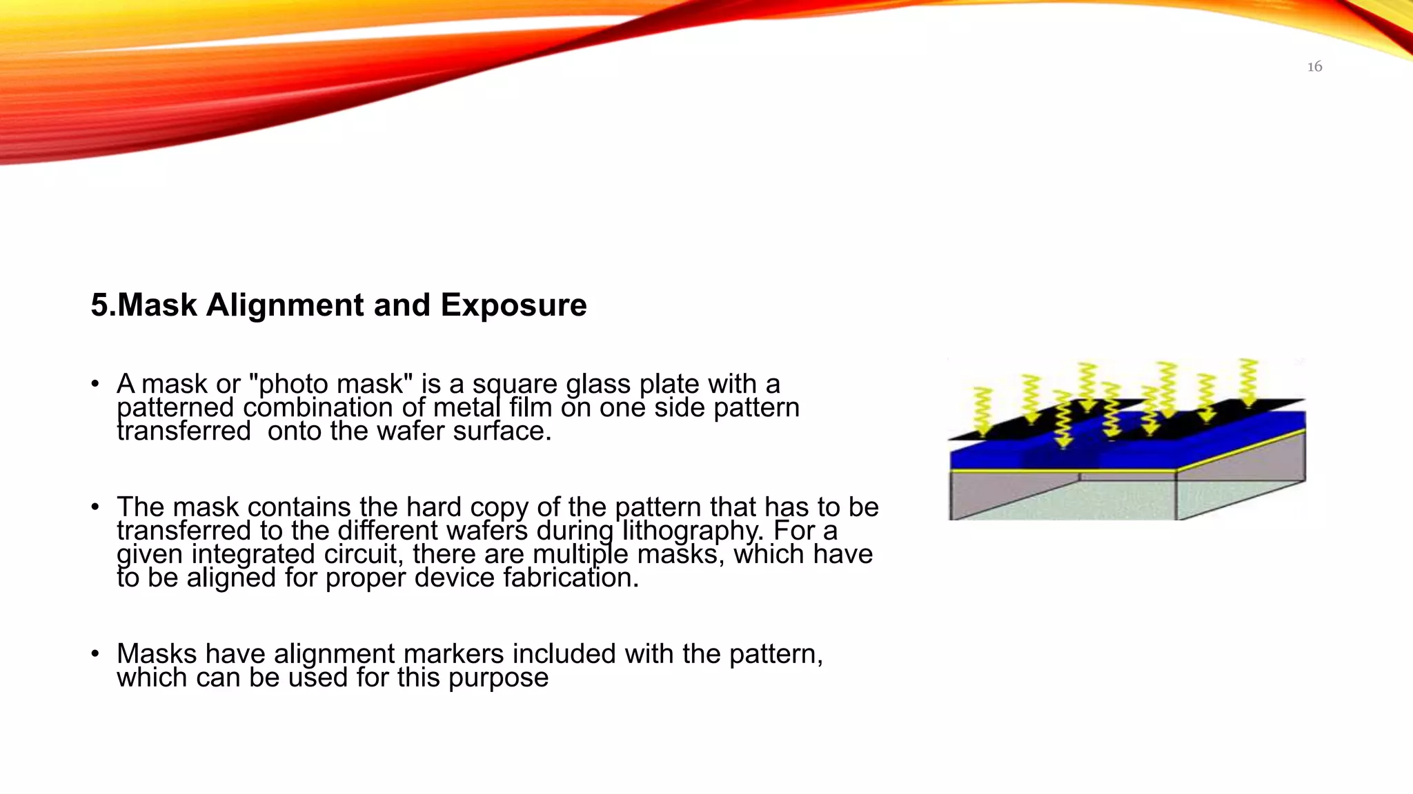
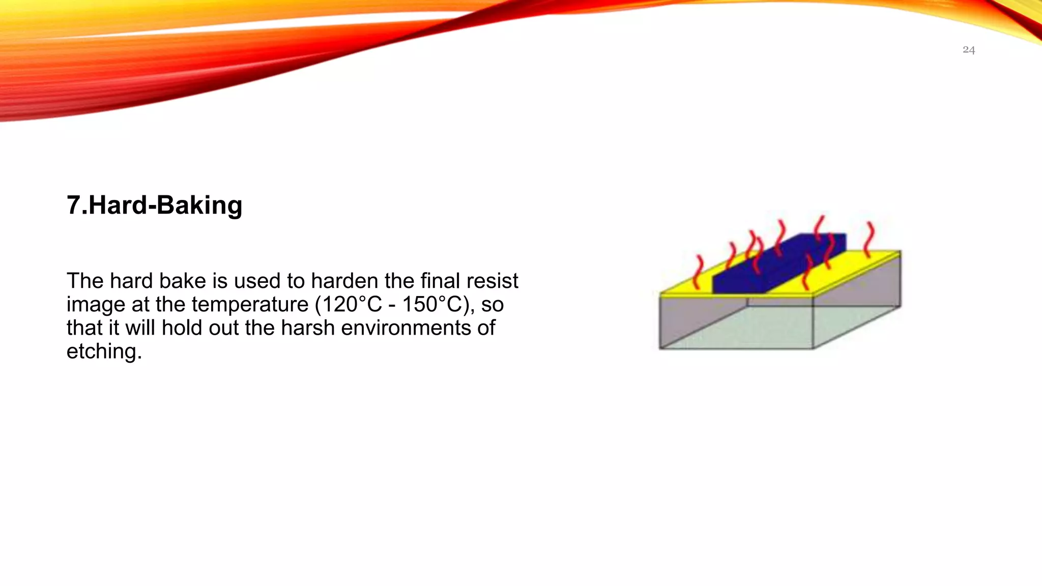
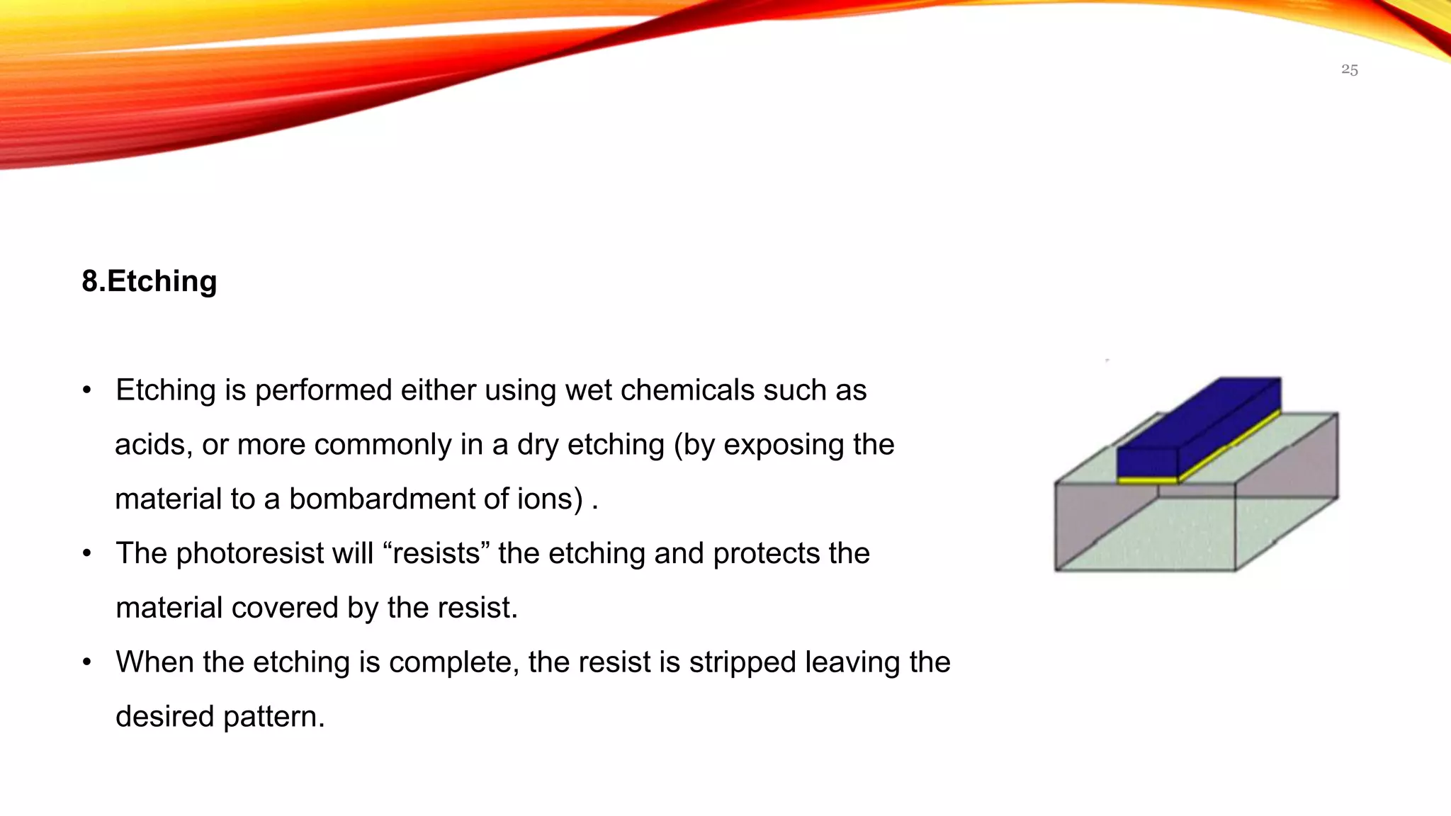
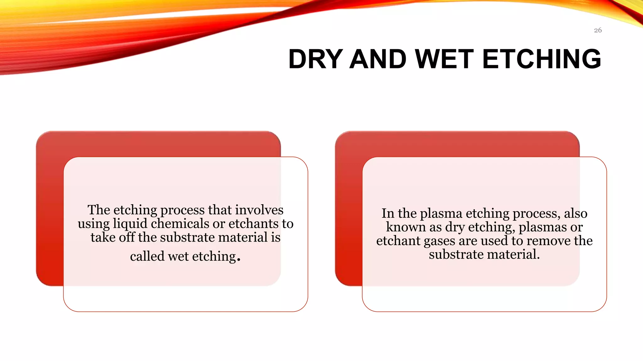
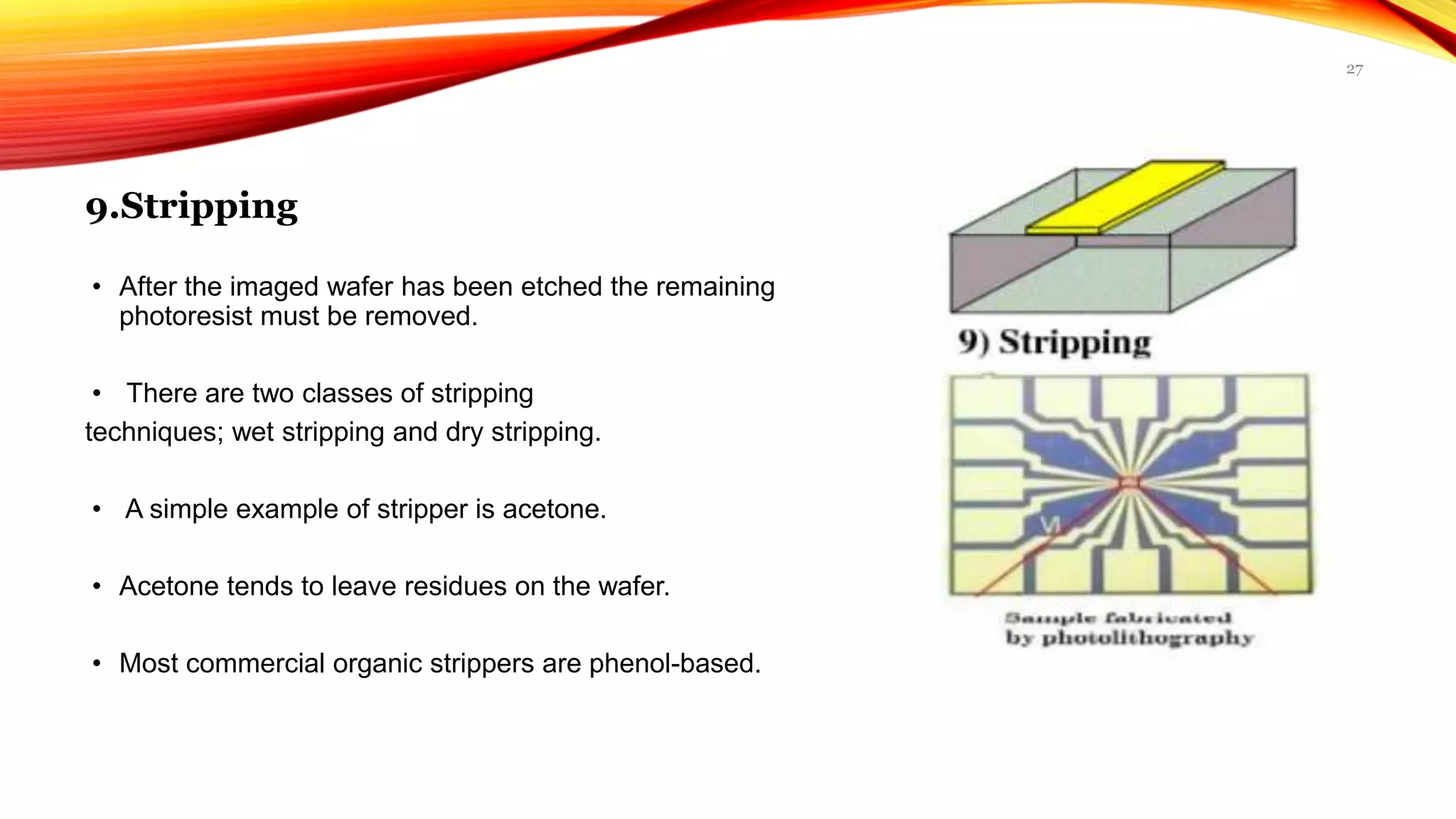
SlideShare a Scribd company logo
LITHOGRAPHY
KAROLINEKERSIN.E
Assistant Professor
1
LITHOGRAPHY IN ART
• Lithography comes from the Greek word, lithos, means "stone“ and graphein, means
"to write”.
• Lithography is a method for printing using a stone (lithographic limestone) with a
completely smooth surface.
• This method was invented in 1796 by German author and actor Alois Senefelder as a
cheap method of publishing artwork on paper or to print text. Lithography works
because of the mutual repulsion of oil and water.
• The image is drawn on the surface of the print plate with a fat or oil-based medium
such as a wax crayon, which may be pigmented to make the drawing visible.
2
LITHOGRAPHY IN IC
FABRICATION
• Lithography (or patterning) refers to the series of steps that establish the shapes,
dimensions, and location of the various components of the integrated circuit (IC).
• The current progress in IC design, with the decreased dimensions (miniaturization) of the
chip and increased density of transistors, is possible only if smaller areas on the wafer
surface can be patterned.
• This is primarily the function of lithography.
• Thus, the success of modern IC design is due largely to lithography.
3
CONTD..
• Create a pattern with the dimensions established by the circuit design.
• Place the pattern correctly with respect to the crystal orientation and
other existing patterns.
• After the pattern is created, either the defined part of the wafer surface
is removed (trench creation) or left behind (island creation) or new
material is deposited.
4
CONTD..
• Lithography is also used to expose certain parts of the wafer surface for doping (either with a
hard mark for thermal diffusion or with a soft mask for ion implantation).
• The correct placement of the circuit pattern involves alignment or registration of various
masks.
• An IC wafer fabrication process can require forty or more patterning steps.
• Alignment of these individual steps is critical to form a working IC.
5
PHOTOLITHOGRAPHY
• Photolithography is the process of transferring geometric
shapes on a mask to the surface of a silicon wafer.
• Photolithography, also called optical lithography or UV
lithography, is a process used in microfabrication to pattern
parts on a thin film or the bulk of a substrate (also called a
wafer)
• Photolithography is a patterning process in which a
photosensitive polymer is selectively exposed to light
through a mask, leaving a latent image in the polymer that
can then be selectively dissolved to provide patterned
access to an underlying substrate.
6
PHOTOLITHOGRAPHY STEPS
7
PHOTOLITHOGRAPHY STEPS:
1 Wafer Cleaning:
In the first step, the wafers are chemically cleaned to remove organic,
ionic, and metallic impurities.
2 Barrier Layer Formation:
After cleaning, silicon dioxide, which serves as a barrier layer, is
deposited on the surface of the wafer.
8
3.Photoresist Application:
• Photoresist is applied to the surface of the wafer by high-speed
centrifugal spinning.
• This technique, known as "Spin Coating," produces a thin uniform
layer of photoresist on the wafer surface.
• In this process a liquid solution of photoresist is give out from the
wafer by rapid spin and produce uniform thin layer (0.5µm to 2.5µm).
• Spin coating/ spinner typically runs at 1200rpm to 4800rpm for 30sec
to 60sec
9
COMPONENTS OF PHOTORESIST
• Polymer - this is a light sensitive polymer whose structure changes on exposure to light. The
desired property is usually change in solubility in a specific solvent.
• Solvent - The solvent is used to thin the resist so that is can be applied on the wafer by a
spin on process. The solvent is usually removed by heating to around 100 ◦C, called soft
bake process.
• Sensitizers - these are used to control the chemical reaction during exposure.
• Additives - various chemicals that are added to achieve specific process results, like dyes.
10
Positive Photoresist:
• Positive photoresists is exposed to UV light, the underlying material
is to be removed.
• In these resists, exposure to the UV light changes the chemical
structure of the resist so that it becomes more soluble in the
developer.
• The exposed resist is then washed away by the developer solution.
In other words, "whatever shows, goes”.
11
CONTD..
• Positive resists directly transfer the pattern from the mask onto the wafer.
• This is because the mask protects the portion of the resist below it from exposure to UV
radiation.
• The rest of the resist, that is exposed, becomes more soluble and can be easily removed.
12
Negative Photoresist:
• Negative photoresists behave in just the opposite
manner. Exposure to the UV light causes the negative resist
to become polymerized, and more difficult to dissolve.
• Therefore, the negative resist remains on the surface
wherever it is exposed, and the developer solution removes
only the unexposed portions.
13
CONTD..
• Negative resists, transfer the negative of the mask pattern to the wafer.
• This is similar to the negative process in film photography.
• For negative resists, the portion that is protected by the mask pattern is more soluble, since
it is not exposed to UV radiation, while the radiation hardens the rest of the resist
14
4.Prebaking
• Prebaking is the step during which almost all of the
solvents are removed from the photoresist.
• The photoresist become photosensitive after
prebaking.
• Photoresist is prebake at 90Co to 100Co for 5min to
30min.
15
5.Mask Alignment and Exposure
• A mask or "photo mask" is a square glass plate with a
patterned combination of metal film on one side pattern
transferred onto the wafer surface.
• The mask contains the hard copy of the pattern that has to be
transferred to the different wafers during lithography. For a
given integrated circuit, there are multiple masks, which have
to be aligned for proper device fabrication.
• Masks have alignment markers included with the pattern,
which can be used for this purpose
16
MASK MAKING
• The alignment markers are usually much smaller than
the typical dimensions of the pattern.
• The mask material is made of borosilicate glass or
quartz with a sputter deposited chrome layer on top.
The chrome layer is 100 nm thick.
• There is also a photoresist layer deposited on top of
the chrome.
• A laser writer is used to ‘write’ the pattern on the mask.
Different laser wavelengths (365, 248 or 193 nm) and
lenses are used to write the pattern on the mask.
• The choice of the wavelength depends on the smallest
dimension on the pattern.
17
• The laser writing process is sequential (line by line) and can take hours depending on the
complexity of the pattern.
• The mask pattern took approximately 7 hours to write, using a 365 nm laser wavelength.
After the pattern is written, a suitable developer is used to remove the unexposed
photoresist.
• After that, the exposed chrome layer is removed (using an acid bath etch) and then the
remaining photoresist is removed to leave behind the chrome desired pattern on glass.
• There are also cleaning and drying steps to remove any excess solvent and keep the mask
free of dust particles
18
METHODS OF MASK ALIGNMENT
There are three primary exposure methods:
• contact
• proximity
• projection.
Contact Printing:
• In contact printing wafer is brought into physical contact with photo
mask. Because of the contact between the resist and mask, very high
resolution is possible.
• The problem with contact printing is that fragments trapped between
the resist and the mask, can damage the mask and cause defects in
the pattern.
19
Projection Printing
• Projection printing avoids mask
damage entirely.
• An image of the patterns on the mask
is projected onto the wafer, which is
many centimeters away.
• To achieve high resolution, only a
small portion of the mask is imaged it
has about 1-micron
20
Proximity Printing
• The proximity exposure method is similar to
contact printing except that a small gap, 10 to 25
microns wide is maintained between the wafer
and the mask.
• This gap minimizes (but may not
eliminate) mask damage.
• Approximately 2 to 4 micron resolution is
• possible with proximity printing
21
6.Development
• Development is a process in which exposed/non-
exposed area is dissolved by developer.
• Most commonly used developer is tetra methyl
ammonium hydroxide is used in concentrations of 0.2 -
0.26.
• Developer is important in controlling the development
uniformity.
22
• Therefore two methods are mainly used i.e. spin development and spray
development.
• During spin development wafers are spun and developer is poured onto the rotating
wafer.
• In spray development, the developer is sprayed rather than poured, on the wafer by
using a nozzle that produces a fine spray over the wafer.
23
7.Hard-Baking
The hard bake is used to harden the final resist
image at the temperature (120°C - 150°C), so
that it will hold out the harsh environments of
etching.
24
8.Etching
• Etching is performed either using wet chemicals such as
acids, or more commonly in a dry etching (by exposing the
material to a bombardment of ions) .
• The photoresist will “resists” the etching and protects the
material covered by the resist.
• When the etching is complete, the resist is stripped leaving the
desired pattern.
25
DRY AND WET ETCHING
The etching process that involves
using liquid chemicals or etchants to
take off the substrate material is
called wet etching.
In the plasma etching process, also
known as dry etching, plasmas or
etchant gases are used to remove the
substrate material.
26
9.Stripping
• After the imaged wafer has been etched the remaining
photoresist must be removed.
• There are two classes of stripping
techniques; wet stripping and dry stripping.
• A simple example of stripper is acetone.
• Acetone tends to leave residues on the wafer.
• Most commercial organic strippers are phenol-based.
27
ADVANTAGES
Photolithography can etch a pattern into an
integrated circuit with a single beam of
ultraviolet light and does not require any
additional materials.
highly efficient
Controls the exact size and shape of the
entire substrate.
28
DISADVANTAGES
Very expensive
Photolithography
requires extremely clean
conditions that are void
of all contaminants,
liquids, and
environmental hazards.
29
APPLICATIONS OF
PHOTOLITHOGRAPHY
• IC designing process
• Fabrication of microcircuits
• Semiconductor industry
• Sensors
• Microprocessor
30
THANK YOU
31

More Related Content

What's hot

X rays lithography
X rays lithographyX rays lithography
X rays lithography
ZUNAIR ARSLAN
 
Electron beam lithography
Electron beam lithographyElectron beam lithography
Electron beam lithography
paneliya sagar
 
photolithography
photolithographyphotolithography
photolithography
Kumar Gaurav
 
Lithography, Photolithography--ABU SYED KUET
Lithography, Photolithography--ABU SYED KUETLithography, Photolithography--ABU SYED KUET
Lithography, Photolithography--ABU SYED KUET
A. S. M. Jannatul Islam
 
Photolithography
PhotolithographyPhotolithography
Photolithography
Melwyn Mayers
 
Etching
EtchingEtching
Etching
Deepak Rawat
 
Etching
Etching Etching
Etching
neha sharma
 
Wafer manufacturing process
Wafer manufacturing processWafer manufacturing process
Wafer manufacturing processadi mandloi
 
Epitaxy
EpitaxyEpitaxy
Epitaxy
ImranAhmad225
 
Oxidation--ABU SYED KUET
Oxidation--ABU SYED KUETOxidation--ABU SYED KUET
Oxidation--ABU SYED KUET
A. S. M. Jannatul Islam
 
Physical Vapour Deposition (PVD)
Physical Vapour Deposition (PVD)Physical Vapour Deposition (PVD)
Physical Vapour Deposition (PVD)
jitendrahemwani
 
08. Micro- & Nano-Fabrication
08. Micro- & Nano-Fabrication08. Micro- & Nano-Fabrication
08. Micro- & Nano-Fabrication
Giuseppe Maruccio
 
Ion implantation
Ion implantationIon implantation
Ion implantation
Adel Niño Iligan
 
photolithography_a
photolithography_aphotolithography_a
photolithography_aguestda8318
 
Nanolithography
NanolithographyNanolithography
Nanolithography
Preeti Choudhary
 
Lithography techniques,types
Lithography techniques,typesLithography techniques,types
Lithography techniques,types
ANJANI S
 
wet etching
wet etchingwet etching
wet etching
tanveer027
 
X-ray lithography
X-ray lithographyX-ray lithography
X-ray lithography
KumarShivam74
 
Ion beam lithography
Ion beam lithographyIon beam lithography
Ion beam lithographyHoang Tien
 

What's hot (20)

X rays lithography
X rays lithographyX rays lithography
X rays lithography
 
Electron beam lithography
Electron beam lithographyElectron beam lithography
Electron beam lithography
 
photolithography
photolithographyphotolithography
photolithography
 
Lithography, Photolithography--ABU SYED KUET
Lithography, Photolithography--ABU SYED KUETLithography, Photolithography--ABU SYED KUET
Lithography, Photolithography--ABU SYED KUET
 
Photolithography
PhotolithographyPhotolithography
Photolithography
 
Etching
EtchingEtching
Etching
 
Etching
Etching Etching
Etching
 
Wafer manufacturing process
Wafer manufacturing processWafer manufacturing process
Wafer manufacturing process
 
Epitaxy
EpitaxyEpitaxy
Epitaxy
 
Oxidation--ABU SYED KUET
Oxidation--ABU SYED KUETOxidation--ABU SYED KUET
Oxidation--ABU SYED KUET
 
Physical Vapour Deposition (PVD)
Physical Vapour Deposition (PVD)Physical Vapour Deposition (PVD)
Physical Vapour Deposition (PVD)
 
Physical vapor deposition
Physical vapor depositionPhysical vapor deposition
Physical vapor deposition
 
08. Micro- & Nano-Fabrication
08. Micro- & Nano-Fabrication08. Micro- & Nano-Fabrication
08. Micro- & Nano-Fabrication
 
Ion implantation
Ion implantationIon implantation
Ion implantation
 
photolithography_a
photolithography_aphotolithography_a
photolithography_a
 
Nanolithography
NanolithographyNanolithography
Nanolithography
 
Lithography techniques,types
Lithography techniques,typesLithography techniques,types
Lithography techniques,types
 
wet etching
wet etchingwet etching
wet etching
 
X-ray lithography
X-ray lithographyX-ray lithography
X-ray lithography
 
Ion beam lithography
Ion beam lithographyIon beam lithography
Ion beam lithography
 

Similar to Photolithography and its procedure

An assignment lithography
An assignment lithographyAn assignment lithography
An assignment lithography
Sagar Dutta
 
Masking and lithography techniques
Masking and lithography techniquesMasking and lithography techniques
Masking and lithography techniques
NivethaBalu5
 
Integrated circuit manufacturing techniques
Integrated circuit manufacturing techniques Integrated circuit manufacturing techniques
Integrated circuit manufacturing techniques
alqohilihamed
 
Mems unit 1-lec_2
Mems unit 1-lec_2Mems unit 1-lec_2
Mems unit 1-lec_2
BRAHMANAND SINGH
 
CMOS Topic 2 -manufacturing_process
CMOS Topic 2 -manufacturing_processCMOS Topic 2 -manufacturing_process
CMOS Topic 2 -manufacturing_process
Ikhwan_Fakrudin
 
Image Transfer Techniques.pptx
Image Transfer Techniques.pptxImage Transfer Techniques.pptx
Image Transfer Techniques.pptx
fikadumola
 
MONOLITHIC IC PROCESSES ppt.pptx
MONOLITHIC IC PROCESSES ppt.pptxMONOLITHIC IC PROCESSES ppt.pptx
MONOLITHIC IC PROCESSES ppt.pptx
ParasSingh894545
 
Nanolithography
NanolithographyNanolithography
Nanolithography
karthika namboothiri
 
Electronic Circuits and PCB Designing - Etching
Electronic Circuits and PCB Designing - EtchingElectronic Circuits and PCB Designing - Etching
Electronic Circuits and PCB Designing - Etching
AnkitMaity
 
nakul agarwal micromachining presentation
nakul agarwal   micromachining presentationnakul agarwal   micromachining presentation
nakul agarwal micromachining presentation
Akash Maurya
 
Photoresist coating
Photoresist coating Photoresist coating
Photoresist coating
Toastmaster International
 
2170508 150110105053,54
2170508 150110105053,542170508 150110105053,54
2170508 150110105053,54
AbhishekThakkar21
 
IC Fabrication Process
IC Fabrication ProcessIC Fabrication Process
IC Fabrication Process
Soudip Sinha Roy
 
Optical exposures
Optical exposuresOptical exposures
Optical exposures
AJAL A J
 
Silicon Manufacturing
Silicon ManufacturingSilicon Manufacturing
Silicon Manufacturing
AJAL A J
 
FILM PROCESSING.pptx
FILM PROCESSING.pptxFILM PROCESSING.pptx
FILM PROCESSING.pptx
Abubakar Hammadama
 
Optical fiber laser
Optical fiber laser Optical fiber laser
Optical fiber laser
Monalisa Mallick
 
Mask fabrication process
Mask fabrication process Mask fabrication process
Mask fabrication process
pardis paliz
 

Similar to Photolithography and its procedure (20)

An assignment lithography
An assignment lithographyAn assignment lithography
An assignment lithography
 
Masking and lithography techniques
Masking and lithography techniquesMasking and lithography techniques
Masking and lithography techniques
 
Integrated circuit manufacturing techniques
Integrated circuit manufacturing techniques Integrated circuit manufacturing techniques
Integrated circuit manufacturing techniques
 
2q
2q2q
2q
 
Mems unit 1-lec_2
Mems unit 1-lec_2Mems unit 1-lec_2
Mems unit 1-lec_2
 
CMOS Topic 2 -manufacturing_process
CMOS Topic 2 -manufacturing_processCMOS Topic 2 -manufacturing_process
CMOS Topic 2 -manufacturing_process
 
Image Transfer Techniques.pptx
Image Transfer Techniques.pptxImage Transfer Techniques.pptx
Image Transfer Techniques.pptx
 
MONOLITHIC IC PROCESSES ppt.pptx
MONOLITHIC IC PROCESSES ppt.pptxMONOLITHIC IC PROCESSES ppt.pptx
MONOLITHIC IC PROCESSES ppt.pptx
 
Nanolithography
NanolithographyNanolithography
Nanolithography
 
Electronic Circuits and PCB Designing - Etching
Electronic Circuits and PCB Designing - EtchingElectronic Circuits and PCB Designing - Etching
Electronic Circuits and PCB Designing - Etching
 
nakul agarwal micromachining presentation
nakul agarwal   micromachining presentationnakul agarwal   micromachining presentation
nakul agarwal micromachining presentation
 
Photoresist coating
Photoresist coating Photoresist coating
Photoresist coating
 
Micromachining
Micromachining Micromachining
Micromachining
 
2170508 150110105053,54
2170508 150110105053,542170508 150110105053,54
2170508 150110105053,54
 
IC Fabrication Process
IC Fabrication ProcessIC Fabrication Process
IC Fabrication Process
 
Optical exposures
Optical exposuresOptical exposures
Optical exposures
 
Silicon Manufacturing
Silicon ManufacturingSilicon Manufacturing
Silicon Manufacturing
 
FILM PROCESSING.pptx
FILM PROCESSING.pptxFILM PROCESSING.pptx
FILM PROCESSING.pptx
 
Optical fiber laser
Optical fiber laser Optical fiber laser
Optical fiber laser
 
Mask fabrication process
Mask fabrication process Mask fabrication process
Mask fabrication process
 

More from karoline Enoch

Thermogravimetric analysis.pptx
Thermogravimetric analysis.pptxThermogravimetric analysis.pptx
Thermogravimetric analysis.pptx
karoline Enoch
 
UV VISIBLE SPECTROSCOPY
UV VISIBLE SPECTROSCOPYUV VISIBLE SPECTROSCOPY
UV VISIBLE SPECTROSCOPY
karoline Enoch
 
Nanotribolgy for medical devices
Nanotribolgy for medical devicesNanotribolgy for medical devices
Nanotribolgy for medical devices
karoline Enoch
 
Protein based nanostructures for biomedical applications
Protein based nanostructures for biomedical applications Protein based nanostructures for biomedical applications
Protein based nanostructures for biomedical applications
karoline Enoch
 
Schering bridge and its derivation
Schering bridge and its derivationSchering bridge and its derivation
Schering bridge and its derivation
karoline Enoch
 
Maxwell bridge and its types
Maxwell bridge and its types Maxwell bridge and its types
Maxwell bridge and its types
karoline Enoch
 
Kelvin bridge and kelvin double bridge
Kelvin bridge and kelvin double bridge Kelvin bridge and kelvin double bridge
Kelvin bridge and kelvin double bridge
karoline Enoch
 
Dc bridge types ,derivation and its application
Dc bridge types ,derivation and its applicationDc bridge types ,derivation and its application
Dc bridge types ,derivation and its application
karoline Enoch
 
Ac bridge and its application
Ac bridge and its application Ac bridge and its application
Ac bridge and its application
karoline Enoch
 
Photodynamic therapy and mechanism
Photodynamic therapy and mechanismPhotodynamic therapy and mechanism
Photodynamic therapy and mechanism
karoline Enoch
 
Preamplifier and impedance matching circuits
Preamplifier and impedance matching circuitsPreamplifier and impedance matching circuits
Preamplifier and impedance matching circuits
karoline Enoch
 
Photo theraphy ,principle and mechanism
Photo theraphy ,principle and mechanismPhoto theraphy ,principle and mechanism
Photo theraphy ,principle and mechanism
karoline Enoch
 
Lasers in opthalmology
Lasers in opthalmologyLasers in opthalmology
Lasers in opthalmology
karoline Enoch
 
Lasers in urology
Lasers in urologyLasers in urology
Lasers in urology
karoline Enoch
 
Lasers in dermatology
Lasers in dermatologyLasers in dermatology
Lasers in dermatology
karoline Enoch
 
Lasers in dentistry
Lasers in dentistryLasers in dentistry
Lasers in dentistry
karoline Enoch
 
Piezoelectric transducer and its working
Piezoelectric transducer and its workingPiezoelectric transducer and its working
Piezoelectric transducer and its working
karoline Enoch
 
Photoelectric transducers and its classification
Photoelectric transducers and its classificationPhotoelectric transducers and its classification
Photoelectric transducers and its classification
karoline Enoch
 
Piezoresistive sensing
Piezoresistive sensingPiezoresistive sensing
Piezoresistive sensing
karoline Enoch
 
Capacitive sensing technology
Capacitive sensing technologyCapacitive sensing technology
Capacitive sensing technology
karoline Enoch
 

More from karoline Enoch (20)

Thermogravimetric analysis.pptx
Thermogravimetric analysis.pptxThermogravimetric analysis.pptx
Thermogravimetric analysis.pptx
 
UV VISIBLE SPECTROSCOPY
UV VISIBLE SPECTROSCOPYUV VISIBLE SPECTROSCOPY
UV VISIBLE SPECTROSCOPY
 
Nanotribolgy for medical devices
Nanotribolgy for medical devicesNanotribolgy for medical devices
Nanotribolgy for medical devices
 
Protein based nanostructures for biomedical applications
Protein based nanostructures for biomedical applications Protein based nanostructures for biomedical applications
Protein based nanostructures for biomedical applications
 
Schering bridge and its derivation
Schering bridge and its derivationSchering bridge and its derivation
Schering bridge and its derivation
 
Maxwell bridge and its types
Maxwell bridge and its types Maxwell bridge and its types
Maxwell bridge and its types
 
Kelvin bridge and kelvin double bridge
Kelvin bridge and kelvin double bridge Kelvin bridge and kelvin double bridge
Kelvin bridge and kelvin double bridge
 
Dc bridge types ,derivation and its application
Dc bridge types ,derivation and its applicationDc bridge types ,derivation and its application
Dc bridge types ,derivation and its application
 
Ac bridge and its application
Ac bridge and its application Ac bridge and its application
Ac bridge and its application
 
Photodynamic therapy and mechanism
Photodynamic therapy and mechanismPhotodynamic therapy and mechanism
Photodynamic therapy and mechanism
 
Preamplifier and impedance matching circuits
Preamplifier and impedance matching circuitsPreamplifier and impedance matching circuits
Preamplifier and impedance matching circuits
 
Photo theraphy ,principle and mechanism
Photo theraphy ,principle and mechanismPhoto theraphy ,principle and mechanism
Photo theraphy ,principle and mechanism
 
Lasers in opthalmology
Lasers in opthalmologyLasers in opthalmology
Lasers in opthalmology
 
Lasers in urology
Lasers in urologyLasers in urology
Lasers in urology
 
Lasers in dermatology
Lasers in dermatologyLasers in dermatology
Lasers in dermatology
 
Lasers in dentistry
Lasers in dentistryLasers in dentistry
Lasers in dentistry
 
Piezoelectric transducer and its working
Piezoelectric transducer and its workingPiezoelectric transducer and its working
Piezoelectric transducer and its working
 
Photoelectric transducers and its classification
Photoelectric transducers and its classificationPhotoelectric transducers and its classification
Photoelectric transducers and its classification
 
Piezoresistive sensing
Piezoresistive sensingPiezoresistive sensing
Piezoresistive sensing
 
Capacitive sensing technology
Capacitive sensing technologyCapacitive sensing technology
Capacitive sensing technology
 

Recently uploaded

Gen AI Study Jams _ For the GDSC Leads in India.pdf
Gen AI Study Jams _ For the GDSC Leads in India.pdfGen AI Study Jams _ For the GDSC Leads in India.pdf
Gen AI Study Jams _ For the GDSC Leads in India.pdf
gdsczhcet
 
COLLEGE BUS MANAGEMENT SYSTEM PROJECT REPORT.pdf
COLLEGE BUS MANAGEMENT SYSTEM PROJECT REPORT.pdfCOLLEGE BUS MANAGEMENT SYSTEM PROJECT REPORT.pdf
COLLEGE BUS MANAGEMENT SYSTEM PROJECT REPORT.pdf
Kamal Acharya
 
Planning Of Procurement o different goods and services
Planning Of Procurement o different goods and servicesPlanning Of Procurement o different goods and services
Planning Of Procurement o different goods and services
JoytuBarua2
 
Standard Reomte Control Interface - Neometrix
Standard Reomte Control Interface - NeometrixStandard Reomte Control Interface - Neometrix
Standard Reomte Control Interface - Neometrix
Neometrix_Engineering_Pvt_Ltd
 
HYDROPOWER - Hydroelectric power generation
HYDROPOWER - Hydroelectric power generationHYDROPOWER - Hydroelectric power generation
HYDROPOWER - Hydroelectric power generation
Robbie Edward Sayers
 
CME397 Surface Engineering- Professional Elective
CME397 Surface Engineering- Professional ElectiveCME397 Surface Engineering- Professional Elective
CME397 Surface Engineering- Professional Elective
karthi keyan
 
Event Management System Vb Net Project Report.pdf
Event Management System Vb Net  Project Report.pdfEvent Management System Vb Net  Project Report.pdf
Event Management System Vb Net Project Report.pdf
Kamal Acharya
 
ethical hacking-mobile hacking methods.ppt
ethical hacking-mobile hacking methods.pptethical hacking-mobile hacking methods.ppt
ethical hacking-mobile hacking methods.ppt
Jayaprasanna4
 
Architectural Portfolio Sean Lockwood
Architectural Portfolio Sean LockwoodArchitectural Portfolio Sean Lockwood
Architectural Portfolio Sean Lockwood
seandesed
 
Top 10 Oil and Gas Projects in Saudi Arabia 2024.pdf
Top 10 Oil and Gas Projects in Saudi Arabia 2024.pdfTop 10 Oil and Gas Projects in Saudi Arabia 2024.pdf
Top 10 Oil and Gas Projects in Saudi Arabia 2024.pdf
Teleport Manpower Consultant
 
Cosmetic shop management system project report.pdf
Cosmetic shop management system project report.pdfCosmetic shop management system project report.pdf
Cosmetic shop management system project report.pdf
Kamal Acharya
 
TECHNICAL TRAINING MANUAL GENERAL FAMILIARIZATION COURSE
TECHNICAL TRAINING MANUAL   GENERAL FAMILIARIZATION COURSETECHNICAL TRAINING MANUAL   GENERAL FAMILIARIZATION COURSE
TECHNICAL TRAINING MANUAL GENERAL FAMILIARIZATION COURSE
DuvanRamosGarzon1
 
Hybrid optimization of pumped hydro system and solar- Engr. Abdul-Azeez.pdf
Hybrid optimization of pumped hydro system and solar- Engr. Abdul-Azeez.pdfHybrid optimization of pumped hydro system and solar- Engr. Abdul-Azeez.pdf
Hybrid optimization of pumped hydro system and solar- Engr. Abdul-Azeez.pdf
fxintegritypublishin
 
WATER CRISIS and its solutions-pptx 1234
WATER CRISIS and its solutions-pptx 1234WATER CRISIS and its solutions-pptx 1234
WATER CRISIS and its solutions-pptx 1234
AafreenAbuthahir2
 
DESIGN A COTTON SEED SEPARATION MACHINE.docx
DESIGN A COTTON SEED SEPARATION MACHINE.docxDESIGN A COTTON SEED SEPARATION MACHINE.docx
DESIGN A COTTON SEED SEPARATION MACHINE.docx
FluxPrime1
 
一比一原版(SFU毕业证)西蒙菲莎大学毕业证成绩单如何办理
一比一原版(SFU毕业证)西蒙菲莎大学毕业证成绩单如何办理一比一原版(SFU毕业证)西蒙菲莎大学毕业证成绩单如何办理
一比一原版(SFU毕业证)西蒙菲莎大学毕业证成绩单如何办理
bakpo1
 
Courier management system project report.pdf
Courier management system project report.pdfCourier management system project report.pdf
Courier management system project report.pdf
Kamal Acharya
 
J.Yang, ICLR 2024, MLILAB, KAIST AI.pdf
J.Yang,  ICLR 2024, MLILAB, KAIST AI.pdfJ.Yang,  ICLR 2024, MLILAB, KAIST AI.pdf
J.Yang, ICLR 2024, MLILAB, KAIST AI.pdf
MLILAB
 
在线办理(ANU毕业证书)澳洲国立大学毕业证录取通知书一模一样
在线办理(ANU毕业证书)澳洲国立大学毕业证录取通知书一模一样在线办理(ANU毕业证书)澳洲国立大学毕业证录取通知书一模一样
在线办理(ANU毕业证书)澳洲国立大学毕业证录取通知书一模一样
obonagu
 
Final project report on grocery store management system..pdf
Final project report on grocery store management system..pdfFinal project report on grocery store management system..pdf
Final project report on grocery store management system..pdf
Kamal Acharya
 

Recently uploaded (20)

Gen AI Study Jams _ For the GDSC Leads in India.pdf
Gen AI Study Jams _ For the GDSC Leads in India.pdfGen AI Study Jams _ For the GDSC Leads in India.pdf
Gen AI Study Jams _ For the GDSC Leads in India.pdf
 
COLLEGE BUS MANAGEMENT SYSTEM PROJECT REPORT.pdf
COLLEGE BUS MANAGEMENT SYSTEM PROJECT REPORT.pdfCOLLEGE BUS MANAGEMENT SYSTEM PROJECT REPORT.pdf
COLLEGE BUS MANAGEMENT SYSTEM PROJECT REPORT.pdf
 
Planning Of Procurement o different goods and services
Planning Of Procurement o different goods and servicesPlanning Of Procurement o different goods and services
Planning Of Procurement o different goods and services
 
Standard Reomte Control Interface - Neometrix
Standard Reomte Control Interface - NeometrixStandard Reomte Control Interface - Neometrix
Standard Reomte Control Interface - Neometrix
 
HYDROPOWER - Hydroelectric power generation
HYDROPOWER - Hydroelectric power generationHYDROPOWER - Hydroelectric power generation
HYDROPOWER - Hydroelectric power generation
 
CME397 Surface Engineering- Professional Elective
CME397 Surface Engineering- Professional ElectiveCME397 Surface Engineering- Professional Elective
CME397 Surface Engineering- Professional Elective
 
Event Management System Vb Net Project Report.pdf
Event Management System Vb Net  Project Report.pdfEvent Management System Vb Net  Project Report.pdf
Event Management System Vb Net Project Report.pdf
 
ethical hacking-mobile hacking methods.ppt
ethical hacking-mobile hacking methods.pptethical hacking-mobile hacking methods.ppt
ethical hacking-mobile hacking methods.ppt
 
Architectural Portfolio Sean Lockwood
Architectural Portfolio Sean LockwoodArchitectural Portfolio Sean Lockwood
Architectural Portfolio Sean Lockwood
 
Top 10 Oil and Gas Projects in Saudi Arabia 2024.pdf
Top 10 Oil and Gas Projects in Saudi Arabia 2024.pdfTop 10 Oil and Gas Projects in Saudi Arabia 2024.pdf
Top 10 Oil and Gas Projects in Saudi Arabia 2024.pdf
 
Cosmetic shop management system project report.pdf
Cosmetic shop management system project report.pdfCosmetic shop management system project report.pdf
Cosmetic shop management system project report.pdf
 
TECHNICAL TRAINING MANUAL GENERAL FAMILIARIZATION COURSE
TECHNICAL TRAINING MANUAL   GENERAL FAMILIARIZATION COURSETECHNICAL TRAINING MANUAL   GENERAL FAMILIARIZATION COURSE
TECHNICAL TRAINING MANUAL GENERAL FAMILIARIZATION COURSE
 
Hybrid optimization of pumped hydro system and solar- Engr. Abdul-Azeez.pdf
Hybrid optimization of pumped hydro system and solar- Engr. Abdul-Azeez.pdfHybrid optimization of pumped hydro system and solar- Engr. Abdul-Azeez.pdf
Hybrid optimization of pumped hydro system and solar- Engr. Abdul-Azeez.pdf
 
WATER CRISIS and its solutions-pptx 1234
WATER CRISIS and its solutions-pptx 1234WATER CRISIS and its solutions-pptx 1234
WATER CRISIS and its solutions-pptx 1234
 
DESIGN A COTTON SEED SEPARATION MACHINE.docx
DESIGN A COTTON SEED SEPARATION MACHINE.docxDESIGN A COTTON SEED SEPARATION MACHINE.docx
DESIGN A COTTON SEED SEPARATION MACHINE.docx
 
一比一原版(SFU毕业证)西蒙菲莎大学毕业证成绩单如何办理
一比一原版(SFU毕业证)西蒙菲莎大学毕业证成绩单如何办理一比一原版(SFU毕业证)西蒙菲莎大学毕业证成绩单如何办理
一比一原版(SFU毕业证)西蒙菲莎大学毕业证成绩单如何办理
 
Courier management system project report.pdf
Courier management system project report.pdfCourier management system project report.pdf
Courier management system project report.pdf
 
J.Yang, ICLR 2024, MLILAB, KAIST AI.pdf
J.Yang,  ICLR 2024, MLILAB, KAIST AI.pdfJ.Yang,  ICLR 2024, MLILAB, KAIST AI.pdf
J.Yang, ICLR 2024, MLILAB, KAIST AI.pdf
 
在线办理(ANU毕业证书)澳洲国立大学毕业证录取通知书一模一样
在线办理(ANU毕业证书)澳洲国立大学毕业证录取通知书一模一样在线办理(ANU毕业证书)澳洲国立大学毕业证录取通知书一模一样
在线办理(ANU毕业证书)澳洲国立大学毕业证录取通知书一模一样
 
Final project report on grocery store management system..pdf
Final project report on grocery store management system..pdfFinal project report on grocery store management system..pdf
Final project report on grocery store management system..pdf
 

Photolithography and its procedure

  • 2. LITHOGRAPHY IN ART • Lithography comes from the Greek word, lithos, means "stone“ and graphein, means "to write”. • Lithography is a method for printing using a stone (lithographic limestone) with a completely smooth surface. • This method was invented in 1796 by German author and actor Alois Senefelder as a cheap method of publishing artwork on paper or to print text. Lithography works because of the mutual repulsion of oil and water. • The image is drawn on the surface of the print plate with a fat or oil-based medium such as a wax crayon, which may be pigmented to make the drawing visible. 2
  • 3. LITHOGRAPHY IN IC FABRICATION • Lithography (or patterning) refers to the series of steps that establish the shapes, dimensions, and location of the various components of the integrated circuit (IC). • The current progress in IC design, with the decreased dimensions (miniaturization) of the chip and increased density of transistors, is possible only if smaller areas on the wafer surface can be patterned. • This is primarily the function of lithography. • Thus, the success of modern IC design is due largely to lithography. 3
  • 4. CONTD.. • Create a pattern with the dimensions established by the circuit design. • Place the pattern correctly with respect to the crystal orientation and other existing patterns. • After the pattern is created, either the defined part of the wafer surface is removed (trench creation) or left behind (island creation) or new material is deposited. 4
  • 5. CONTD.. • Lithography is also used to expose certain parts of the wafer surface for doping (either with a hard mark for thermal diffusion or with a soft mask for ion implantation). • The correct placement of the circuit pattern involves alignment or registration of various masks. • An IC wafer fabrication process can require forty or more patterning steps. • Alignment of these individual steps is critical to form a working IC. 5
  • 6. PHOTOLITHOGRAPHY • Photolithography is the process of transferring geometric shapes on a mask to the surface of a silicon wafer. • Photolithography, also called optical lithography or UV lithography, is a process used in microfabrication to pattern parts on a thin film or the bulk of a substrate (also called a wafer) • Photolithography is a patterning process in which a photosensitive polymer is selectively exposed to light through a mask, leaving a latent image in the polymer that can then be selectively dissolved to provide patterned access to an underlying substrate. 6
  • 8. PHOTOLITHOGRAPHY STEPS: 1 Wafer Cleaning: In the first step, the wafers are chemically cleaned to remove organic, ionic, and metallic impurities. 2 Barrier Layer Formation: After cleaning, silicon dioxide, which serves as a barrier layer, is deposited on the surface of the wafer. 8
  • 9. 3.Photoresist Application: • Photoresist is applied to the surface of the wafer by high-speed centrifugal spinning. • This technique, known as "Spin Coating," produces a thin uniform layer of photoresist on the wafer surface. • In this process a liquid solution of photoresist is give out from the wafer by rapid spin and produce uniform thin layer (0.5µm to 2.5µm). • Spin coating/ spinner typically runs at 1200rpm to 4800rpm for 30sec to 60sec 9
  • 10. COMPONENTS OF PHOTORESIST • Polymer - this is a light sensitive polymer whose structure changes on exposure to light. The desired property is usually change in solubility in a specific solvent. • Solvent - The solvent is used to thin the resist so that is can be applied on the wafer by a spin on process. The solvent is usually removed by heating to around 100 ◦C, called soft bake process. • Sensitizers - these are used to control the chemical reaction during exposure. • Additives - various chemicals that are added to achieve specific process results, like dyes. 10
  • 11. Positive Photoresist: • Positive photoresists is exposed to UV light, the underlying material is to be removed. • In these resists, exposure to the UV light changes the chemical structure of the resist so that it becomes more soluble in the developer. • The exposed resist is then washed away by the developer solution. In other words, "whatever shows, goes”. 11
  • 12. CONTD.. • Positive resists directly transfer the pattern from the mask onto the wafer. • This is because the mask protects the portion of the resist below it from exposure to UV radiation. • The rest of the resist, that is exposed, becomes more soluble and can be easily removed. 12
  • 13. Negative Photoresist: • Negative photoresists behave in just the opposite manner. Exposure to the UV light causes the negative resist to become polymerized, and more difficult to dissolve. • Therefore, the negative resist remains on the surface wherever it is exposed, and the developer solution removes only the unexposed portions. 13
  • 14. CONTD.. • Negative resists, transfer the negative of the mask pattern to the wafer. • This is similar to the negative process in film photography. • For negative resists, the portion that is protected by the mask pattern is more soluble, since it is not exposed to UV radiation, while the radiation hardens the rest of the resist 14
  • 15. 4.Prebaking • Prebaking is the step during which almost all of the solvents are removed from the photoresist. • The photoresist become photosensitive after prebaking. • Photoresist is prebake at 90Co to 100Co for 5min to 30min. 15
  • 16. 5.Mask Alignment and Exposure • A mask or "photo mask" is a square glass plate with a patterned combination of metal film on one side pattern transferred onto the wafer surface. • The mask contains the hard copy of the pattern that has to be transferred to the different wafers during lithography. For a given integrated circuit, there are multiple masks, which have to be aligned for proper device fabrication. • Masks have alignment markers included with the pattern, which can be used for this purpose 16
  • 17. MASK MAKING • The alignment markers are usually much smaller than the typical dimensions of the pattern. • The mask material is made of borosilicate glass or quartz with a sputter deposited chrome layer on top. The chrome layer is 100 nm thick. • There is also a photoresist layer deposited on top of the chrome. • A laser writer is used to ‘write’ the pattern on the mask. Different laser wavelengths (365, 248 or 193 nm) and lenses are used to write the pattern on the mask. • The choice of the wavelength depends on the smallest dimension on the pattern. 17
  • 18. • The laser writing process is sequential (line by line) and can take hours depending on the complexity of the pattern. • The mask pattern took approximately 7 hours to write, using a 365 nm laser wavelength. After the pattern is written, a suitable developer is used to remove the unexposed photoresist. • After that, the exposed chrome layer is removed (using an acid bath etch) and then the remaining photoresist is removed to leave behind the chrome desired pattern on glass. • There are also cleaning and drying steps to remove any excess solvent and keep the mask free of dust particles 18
  • 19. METHODS OF MASK ALIGNMENT There are three primary exposure methods: • contact • proximity • projection. Contact Printing: • In contact printing wafer is brought into physical contact with photo mask. Because of the contact between the resist and mask, very high resolution is possible. • The problem with contact printing is that fragments trapped between the resist and the mask, can damage the mask and cause defects in the pattern. 19
  • 20. Projection Printing • Projection printing avoids mask damage entirely. • An image of the patterns on the mask is projected onto the wafer, which is many centimeters away. • To achieve high resolution, only a small portion of the mask is imaged it has about 1-micron 20
  • 21. Proximity Printing • The proximity exposure method is similar to contact printing except that a small gap, 10 to 25 microns wide is maintained between the wafer and the mask. • This gap minimizes (but may not eliminate) mask damage. • Approximately 2 to 4 micron resolution is • possible with proximity printing 21
  • 22. 6.Development • Development is a process in which exposed/non- exposed area is dissolved by developer. • Most commonly used developer is tetra methyl ammonium hydroxide is used in concentrations of 0.2 - 0.26. • Developer is important in controlling the development uniformity. 22
  • 23. • Therefore two methods are mainly used i.e. spin development and spray development. • During spin development wafers are spun and developer is poured onto the rotating wafer. • In spray development, the developer is sprayed rather than poured, on the wafer by using a nozzle that produces a fine spray over the wafer. 23
  • 24. 7.Hard-Baking The hard bake is used to harden the final resist image at the temperature (120°C - 150°C), so that it will hold out the harsh environments of etching. 24
  • 25. 8.Etching • Etching is performed either using wet chemicals such as acids, or more commonly in a dry etching (by exposing the material to a bombardment of ions) . • The photoresist will “resists” the etching and protects the material covered by the resist. • When the etching is complete, the resist is stripped leaving the desired pattern. 25
  • 26. DRY AND WET ETCHING The etching process that involves using liquid chemicals or etchants to take off the substrate material is called wet etching. In the plasma etching process, also known as dry etching, plasmas or etchant gases are used to remove the substrate material. 26
  • 27. 9.Stripping • After the imaged wafer has been etched the remaining photoresist must be removed. • There are two classes of stripping techniques; wet stripping and dry stripping. • A simple example of stripper is acetone. • Acetone tends to leave residues on the wafer. • Most commercial organic strippers are phenol-based. 27
  • 28. ADVANTAGES Photolithography can etch a pattern into an integrated circuit with a single beam of ultraviolet light and does not require any additional materials. highly efficient Controls the exact size and shape of the entire substrate. 28
  • 29. DISADVANTAGES Very expensive Photolithography requires extremely clean conditions that are void of all contaminants, liquids, and environmental hazards. 29
  • 30. APPLICATIONS OF PHOTOLITHOGRAPHY • IC designing process • Fabrication of microcircuits • Semiconductor industry • Sensors • Microprocessor 30