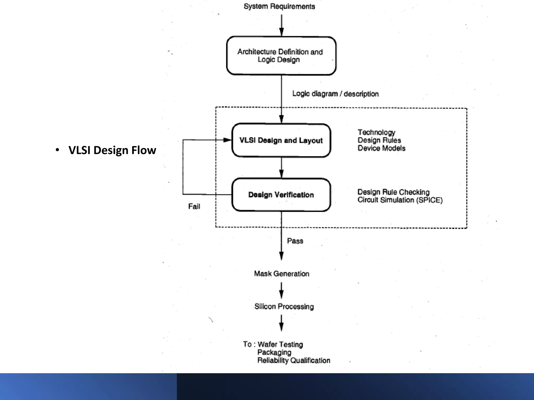
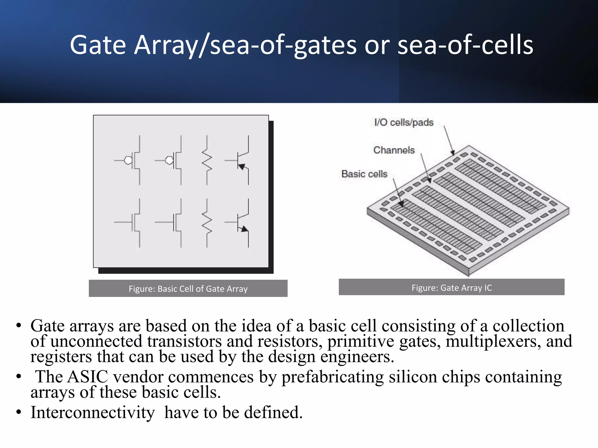
SlideShare a Scribd company logo
MOSFET: History, Trends and
Structure
References
Weste: Introduction
Kang: MOS System
• It is a well-known premise in
engineering that the conception of a
complex construction
• without a prior understanding of the
underlying building blocks is a sure
road to failure.
• This surely holds for digital circuit
design as well
Introduction
• It is a well-known
premise in
engineering that the
conception of a
complex construction
without a prior
understanding of the
underlying building
blocks is a sure road
to failure.
• This surely holds for
digital circuit design
as well
• The basic building blocks in today’s
digital circuits are the silicon
semiconductor devices, more
specifically the MOS transistors
and to a lesser degree the parasitic
diodes, and the interconnect wires.
• The role of the semiconductor
devices has been appreciated for a
long time in the world of digital
integrated circuits. On the other
hand, interconnect wires have only
recently started to play a dominant
role as a result of the advanced
scaling of the semiconductor
technology.
Feature Size/Technology Node
The feature size of a CMOS manufacturing process
refers to the minimum dimension of a transistor
(channel length) that can be reliably built.
The 4004 processor had a feature size of 10 µm in
1971. The Core-2 Duo had a feature size of 45 nm in
2008.
 Manufacturers introduce a new process generation
known as a technology node every 2–3 years with a ~30%
smaller feature
Figure: Process Generations
Moore’s Law
• In 1965, Gordon Moore observed that plotting the number of transistors that can be
economically manufactured on chip gives a straight line on a semilogarithmic scale.
• At the time, he found transistor count doubling every 18 months.
• This observation is called Moore’s Law .
• Moore’s Law is driven primarily by scaling down the size of transistors and, to a
minor extent, by building larger chips.
• In 1947, John Bardeen and Walter
Brattain built the first functioning
point contact transistor at Bell
Laboratories, shown in Figure (left)
(won Noble Prize in 1956)
• Ten years later, Jack Kilby at Texas
Instruments realized the potential
for miniaturization. Figure (right)
shows his first prototype of an
integrated circuit, constructed from
a germanium slice and gold wires.
(won Noble Prize in 2000)
History and Trend
History and Trend
• In 1958, Jack Kilby built the first integrated circuit with two
transistors at Texas Instruments.
• In 2008, Intel’s microprocessor contained more than 2 billion
transistors and a 16 GB Flash memory contained more than 4
billion transistors.
• This corresponds to a compound annual growth rate of 53% over
50 years.
• No other technology in history has sustained such a high growth
rate lasting for so long.
This incredible growth has come from
steady miniaturization of transistors and
improvements in manufacturing processes.
Transistor
•Transistors can be viewed as electrically controlled switches with a
control terminal and two other terminals that are connected or
disconnected depending on the voltage or current applied to the
control.
•Bipolar transistors require a small current into the control (base)
terminal to switch much larger currents between the other two
(emitter and collector) terminals.
•The quiescent power dissipated by these base currents, drawn even
when the circuit is not switching, limits the maximum number of
transistors that can be integrated onto a single die.
Bipolar Transistors
MOSFETs
The original idea of FET dated back to the German scientist Julius Lilienfield in
1925 [US patent 1,745,175] and a structure closely resembling the MOSFET
was proposed in 1935 by Oskar Heil [British patent 439,457], but materials
problems foiled early attempts to make functioning devices.
By the 1960s, Metal Oxide Semiconductor Field Effect Transistors (MOSFETs)
began to enter production.
MOSFETs offer the compelling advantage that they draw almost zero control
current while idle.
Metal Oxide Semiconductor Field Effect Transistors (MOSFETs)
Key Developments
In 1963, Frank Wanlass at Fairchild described the first logic gates using
MOSFETs [Wanlass63].
Fairchild’s gates used both nMOS and pMOS transistors, earning the
name Complementary Metal Oxide Semiconductor, or CMOS.
The circuits used discrete MOSFET’s but consumed only nanowatts of
power, six orders of magnitude less than their bipolar counterparts.
With the development of the silicon planar process, MOS integrated
circuits became attractive for their low cost because the fabrication process
was simpler
Scale of Integration
• Small-scale integration (SSI) circuits: such as the 7404 inverter, have fewer
than 10 gates, with roughly half a dozen transistors per gate.
• Medium-scale integration (MSI) circuits, such as the 74161 counter, have
up to 1000 gates.
• Large-scale integration (LSI) circuits, such as simple 8-bit
microprocessors, have up to 10,000 gates.
• Very Large-Scale Integration (VLSI) Circuits: It soon became apparent that
new names would have to be created every five years if this naming trend
continued and thus the term Very Large-Scale Integration (VLSI) is used to
describe most integrated circuits from the 1980s onward.
• VLSI Design Flow
Application Specific Integrated Circuit (ASIC)
An application-specific integrated circuit (ASIC) is a microchip
designed for a special application, such as a kind of transmission
protocol or a hand-held computer.
ASICs can broadly be classified as:
1. Full Custom ASIC
2. Gate Array ASIC
Application-Specific Integrated Circuit
Full Custom
Design
• The ASIC vendor does not prefabricate
any components on the silicon and does
not provide any libraries of predefined
logic gates and functions.
• By means of appropriate tools, the
engineers can handcraft the dimensions
of individual transistors and then create
higher-level functions based on these
elements.
• For example, if the engineers require a
slightly faster logic gate, they can alter
the dimensions of the transistors used to
build that gate.
• The design of full-custom devices is
complex and time-consuming, but the
resulting chips contain the maximum
amount of logic with minimal waste of
silicon real estate.
• Gate arrays are based on the idea of a basic cell consisting of a collection
of unconnected transistors and resistors, primitive gates, multiplexers, and
registers that can be used by the design engineers.
• The ASIC vendor commences by prefabricating silicon chips containing
arrays of these basic cells.
• Interconnectivity have to be defined.
Figure: Gate Array IC
Figure: Basic Cell of Gate Array
Gate Array/sea-of-gates or sea-of-cells
VLSI Trends.pptx

More Related Content

Similar to VLSI Trends.pptx

Semiconductor-based transistors (1).pptx
Semiconductor-based transistors (1).pptxSemiconductor-based transistors (1).pptx
Semiconductor-based transistors (1).pptx
HasanHasani18
 
Presentationvlsi converted
Presentationvlsi convertedPresentationvlsi converted
Presentationvlsi converted
vijayakumar sivaji
 
vlsi_12.pdf
vlsi_12.pdfvlsi_12.pdf
vlsi_12.pdf
AcademicICECE
 
Integrated circuit
Integrated circuitIntegrated circuit
Integrated circuit
jhamapits
 
integrated circuits
integrated circuitsintegrated circuits
integrated circuits
AJAL A J
 
SISTec Microelectronics VLSI design
SISTec Microelectronics VLSI designSISTec Microelectronics VLSI design
SISTec Microelectronics VLSI design
Dr. Ravi Mishra
 
ppt on IC [Integrated Circuit]
ppt on IC [Integrated Circuit]ppt on IC [Integrated Circuit]
ppt on IC [Integrated Circuit]
Riddhi Patel
 
EC6601 VLSI Design CMOS Fabrication
EC6601 VLSI Design   CMOS FabricationEC6601 VLSI Design   CMOS Fabrication
EC6601 VLSI Design CMOS Fabrication
chitrarengasamy
 
5_DVD_VLSI Technology Trends.pdf
5_DVD_VLSI Technology Trends.pdf5_DVD_VLSI Technology Trends.pdf
5_DVD_VLSI Technology Trends.pdf
Usha Mehta
 
chapter 1.ppt
chapter 1.pptchapter 1.ppt
chapter 1.ppt
ssuser6f92bc
 
Integrated circuit
Integrated circuitIntegrated circuit
Integrated circuit
Daniella Glean
 
Vlsi design
Vlsi designVlsi design
Vlsi design
Iftikar Alam
 
Vlsi
VlsiVlsi
Vlsi
soumya968
 
Third generation of computer
Third generation of computerThird generation of computer
Third generation of computer
Norhaina Abdulkadir
 
Vlsi td introduction
Vlsi td introductionVlsi td introduction
Vlsi td introduction
Govinda Prasad Acharya
 
VLSI unit 1 Technology - S.ppt
VLSI unit 1 Technology - S.pptVLSI unit 1 Technology - S.ppt
VLSI unit 1 Technology - S.ppt
indrajeetPatel22
 
1 VLSI Introduction.pptx
1 VLSI Introduction.pptx1 VLSI Introduction.pptx
1 VLSI Introduction.pptx
ShishirAhmed39
 
kbaps_VLSI
kbaps_VLSIkbaps_VLSI
Asic &fpga
Asic &fpgaAsic &fpga
Asic &fpga
Podili Ramu
 
Silicon to software share
Silicon to software shareSilicon to software share
Silicon to software share
Narendra Patel
 

Similar to VLSI Trends.pptx (20)

Semiconductor-based transistors (1).pptx
Semiconductor-based transistors (1).pptxSemiconductor-based transistors (1).pptx
Semiconductor-based transistors (1).pptx
 
Presentationvlsi converted
Presentationvlsi convertedPresentationvlsi converted
Presentationvlsi converted
 
vlsi_12.pdf
vlsi_12.pdfvlsi_12.pdf
vlsi_12.pdf
 
Integrated circuit
Integrated circuitIntegrated circuit
Integrated circuit
 
integrated circuits
integrated circuitsintegrated circuits
integrated circuits
 
SISTec Microelectronics VLSI design
SISTec Microelectronics VLSI designSISTec Microelectronics VLSI design
SISTec Microelectronics VLSI design
 
ppt on IC [Integrated Circuit]
ppt on IC [Integrated Circuit]ppt on IC [Integrated Circuit]
ppt on IC [Integrated Circuit]
 
EC6601 VLSI Design CMOS Fabrication
EC6601 VLSI Design   CMOS FabricationEC6601 VLSI Design   CMOS Fabrication
EC6601 VLSI Design CMOS Fabrication
 
5_DVD_VLSI Technology Trends.pdf
5_DVD_VLSI Technology Trends.pdf5_DVD_VLSI Technology Trends.pdf
5_DVD_VLSI Technology Trends.pdf
 
chapter 1.ppt
chapter 1.pptchapter 1.ppt
chapter 1.ppt
 
Integrated circuit
Integrated circuitIntegrated circuit
Integrated circuit
 
Vlsi design
Vlsi designVlsi design
Vlsi design
 
Vlsi
VlsiVlsi
Vlsi
 
Third generation of computer
Third generation of computerThird generation of computer
Third generation of computer
 
Vlsi td introduction
Vlsi td introductionVlsi td introduction
Vlsi td introduction
 
VLSI unit 1 Technology - S.ppt
VLSI unit 1 Technology - S.pptVLSI unit 1 Technology - S.ppt
VLSI unit 1 Technology - S.ppt
 
1 VLSI Introduction.pptx
1 VLSI Introduction.pptx1 VLSI Introduction.pptx
1 VLSI Introduction.pptx
 
kbaps_VLSI
kbaps_VLSIkbaps_VLSI
kbaps_VLSI
 
Asic &fpga
Asic &fpgaAsic &fpga
Asic &fpga
 
Silicon to software share
Silicon to software shareSilicon to software share
Silicon to software share
 

Recently uploaded

sieving analysis and results interpretation
sieving analysis and results interpretationsieving analysis and results interpretation
sieving analysis and results interpretation
ssuser36d3051
 
Embedded machine learning-based road conditions and driving behavior monitoring
Embedded machine learning-based road conditions and driving behavior monitoringEmbedded machine learning-based road conditions and driving behavior monitoring
Embedded machine learning-based road conditions and driving behavior monitoring
IJECEIAES
 
Understanding Inductive Bias in Machine Learning
Understanding Inductive Bias in Machine LearningUnderstanding Inductive Bias in Machine Learning
Understanding Inductive Bias in Machine Learning
SUTEJAS
 
ACEP Magazine edition 4th launched on 05.06.2024
ACEP Magazine edition 4th launched on 05.06.2024ACEP Magazine edition 4th launched on 05.06.2024
ACEP Magazine edition 4th launched on 05.06.2024
Rahul
 
5214-1693458878915-Unit 6 2023 to 2024 academic year assignment (AutoRecovere...
5214-1693458878915-Unit 6 2023 to 2024 academic year assignment (AutoRecovere...5214-1693458878915-Unit 6 2023 to 2024 academic year assignment (AutoRecovere...
5214-1693458878915-Unit 6 2023 to 2024 academic year assignment (AutoRecovere...
ihlasbinance2003
 
Harnessing WebAssembly for Real-time Stateless Streaming Pipelines
Harnessing WebAssembly for Real-time Stateless Streaming PipelinesHarnessing WebAssembly for Real-time Stateless Streaming Pipelines
Harnessing WebAssembly for Real-time Stateless Streaming Pipelines
Christina Lin
 
Low power architecture of logic gates using adiabatic techniques
Low power architecture of logic gates using adiabatic techniquesLow power architecture of logic gates using adiabatic techniques
Low power architecture of logic gates using adiabatic techniques
nooriasukmaningtyas
 
spirit beverages ppt without graphics.pptx
spirit beverages ppt without graphics.pptxspirit beverages ppt without graphics.pptx
spirit beverages ppt without graphics.pptx
Madan Karki
 
Recycled Concrete Aggregate in Construction Part III
Recycled Concrete Aggregate in Construction Part IIIRecycled Concrete Aggregate in Construction Part III
Recycled Concrete Aggregate in Construction Part III
Aditya Rajan Patra
 
Literature Review Basics and Understanding Reference Management.pptx
Literature Review Basics and Understanding Reference Management.pptxLiterature Review Basics and Understanding Reference Management.pptx
Literature Review Basics and Understanding Reference Management.pptx
Dr Ramhari Poudyal
 
Properties Railway Sleepers and Test.pptx
Properties Railway Sleepers and Test.pptxProperties Railway Sleepers and Test.pptx
Properties Railway Sleepers and Test.pptx
MDSABBIROJJAMANPAYEL
 
DEEP LEARNING FOR SMART GRID INTRUSION DETECTION: A HYBRID CNN-LSTM-BASED MODEL
DEEP LEARNING FOR SMART GRID INTRUSION DETECTION: A HYBRID CNN-LSTM-BASED MODELDEEP LEARNING FOR SMART GRID INTRUSION DETECTION: A HYBRID CNN-LSTM-BASED MODEL
DEEP LEARNING FOR SMART GRID INTRUSION DETECTION: A HYBRID CNN-LSTM-BASED MODEL
gerogepatton
 
digital fundamental by Thomas L.floydl.pdf
digital fundamental by Thomas L.floydl.pdfdigital fundamental by Thomas L.floydl.pdf
digital fundamental by Thomas L.floydl.pdf
drwaing
 
Wearable antenna for antenna applications
Wearable antenna for antenna applicationsWearable antenna for antenna applications
Wearable antenna for antenna applications
Madhumitha Jayaram
 
ACRP 4-09 Risk Assessment Method to Support Modification of Airfield Separat...
ACRP 4-09 Risk Assessment Method to Support Modification of Airfield Separat...ACRP 4-09 Risk Assessment Method to Support Modification of Airfield Separat...
ACRP 4-09 Risk Assessment Method to Support Modification of Airfield Separat...
Mukeshwaran Balu
 
IEEE Aerospace and Electronic Systems Society as a Graduate Student Member
IEEE Aerospace and Electronic Systems Society as a Graduate Student MemberIEEE Aerospace and Electronic Systems Society as a Graduate Student Member
IEEE Aerospace and Electronic Systems Society as a Graduate Student Member
VICTOR MAESTRE RAMIREZ
 
International Conference on NLP, Artificial Intelligence, Machine Learning an...
International Conference on NLP, Artificial Intelligence, Machine Learning an...International Conference on NLP, Artificial Intelligence, Machine Learning an...
International Conference on NLP, Artificial Intelligence, Machine Learning an...
gerogepatton
 
Presentation of IEEE Slovenia CIS (Computational Intelligence Society) Chapte...
Presentation of IEEE Slovenia CIS (Computational Intelligence Society) Chapte...Presentation of IEEE Slovenia CIS (Computational Intelligence Society) Chapte...
Presentation of IEEE Slovenia CIS (Computational Intelligence Society) Chapte...
University of Maribor
 
A SYSTEMATIC RISK ASSESSMENT APPROACH FOR SECURING THE SMART IRRIGATION SYSTEMS
A SYSTEMATIC RISK ASSESSMENT APPROACH FOR SECURING THE SMART IRRIGATION SYSTEMSA SYSTEMATIC RISK ASSESSMENT APPROACH FOR SECURING THE SMART IRRIGATION SYSTEMS
A SYSTEMATIC RISK ASSESSMENT APPROACH FOR SECURING THE SMART IRRIGATION SYSTEMS
IJNSA Journal
 
哪里办理(csu毕业证书)查尔斯特大学毕业证硕士学历原版一模一样
哪里办理(csu毕业证书)查尔斯特大学毕业证硕士学历原版一模一样哪里办理(csu毕业证书)查尔斯特大学毕业证硕士学历原版一模一样
哪里办理(csu毕业证书)查尔斯特大学毕业证硕士学历原版一模一样
insn4465
 

Recently uploaded (20)

sieving analysis and results interpretation
sieving analysis and results interpretationsieving analysis and results interpretation
sieving analysis and results interpretation
 
Embedded machine learning-based road conditions and driving behavior monitoring
Embedded machine learning-based road conditions and driving behavior monitoringEmbedded machine learning-based road conditions and driving behavior monitoring
Embedded machine learning-based road conditions and driving behavior monitoring
 
Understanding Inductive Bias in Machine Learning
Understanding Inductive Bias in Machine LearningUnderstanding Inductive Bias in Machine Learning
Understanding Inductive Bias in Machine Learning
 
ACEP Magazine edition 4th launched on 05.06.2024
ACEP Magazine edition 4th launched on 05.06.2024ACEP Magazine edition 4th launched on 05.06.2024
ACEP Magazine edition 4th launched on 05.06.2024
 
5214-1693458878915-Unit 6 2023 to 2024 academic year assignment (AutoRecovere...
5214-1693458878915-Unit 6 2023 to 2024 academic year assignment (AutoRecovere...5214-1693458878915-Unit 6 2023 to 2024 academic year assignment (AutoRecovere...
5214-1693458878915-Unit 6 2023 to 2024 academic year assignment (AutoRecovere...
 
Harnessing WebAssembly for Real-time Stateless Streaming Pipelines
Harnessing WebAssembly for Real-time Stateless Streaming PipelinesHarnessing WebAssembly for Real-time Stateless Streaming Pipelines
Harnessing WebAssembly for Real-time Stateless Streaming Pipelines
 
Low power architecture of logic gates using adiabatic techniques
Low power architecture of logic gates using adiabatic techniquesLow power architecture of logic gates using adiabatic techniques
Low power architecture of logic gates using adiabatic techniques
 
spirit beverages ppt without graphics.pptx
spirit beverages ppt without graphics.pptxspirit beverages ppt without graphics.pptx
spirit beverages ppt without graphics.pptx
 
Recycled Concrete Aggregate in Construction Part III
Recycled Concrete Aggregate in Construction Part IIIRecycled Concrete Aggregate in Construction Part III
Recycled Concrete Aggregate in Construction Part III
 
Literature Review Basics and Understanding Reference Management.pptx
Literature Review Basics and Understanding Reference Management.pptxLiterature Review Basics and Understanding Reference Management.pptx
Literature Review Basics and Understanding Reference Management.pptx
 
Properties Railway Sleepers and Test.pptx
Properties Railway Sleepers and Test.pptxProperties Railway Sleepers and Test.pptx
Properties Railway Sleepers and Test.pptx
 
DEEP LEARNING FOR SMART GRID INTRUSION DETECTION: A HYBRID CNN-LSTM-BASED MODEL
DEEP LEARNING FOR SMART GRID INTRUSION DETECTION: A HYBRID CNN-LSTM-BASED MODELDEEP LEARNING FOR SMART GRID INTRUSION DETECTION: A HYBRID CNN-LSTM-BASED MODEL
DEEP LEARNING FOR SMART GRID INTRUSION DETECTION: A HYBRID CNN-LSTM-BASED MODEL
 
digital fundamental by Thomas L.floydl.pdf
digital fundamental by Thomas L.floydl.pdfdigital fundamental by Thomas L.floydl.pdf
digital fundamental by Thomas L.floydl.pdf
 
Wearable antenna for antenna applications
Wearable antenna for antenna applicationsWearable antenna for antenna applications
Wearable antenna for antenna applications
 
ACRP 4-09 Risk Assessment Method to Support Modification of Airfield Separat...
ACRP 4-09 Risk Assessment Method to Support Modification of Airfield Separat...ACRP 4-09 Risk Assessment Method to Support Modification of Airfield Separat...
ACRP 4-09 Risk Assessment Method to Support Modification of Airfield Separat...
 
IEEE Aerospace and Electronic Systems Society as a Graduate Student Member
IEEE Aerospace and Electronic Systems Society as a Graduate Student MemberIEEE Aerospace and Electronic Systems Society as a Graduate Student Member
IEEE Aerospace and Electronic Systems Society as a Graduate Student Member
 
International Conference on NLP, Artificial Intelligence, Machine Learning an...
International Conference on NLP, Artificial Intelligence, Machine Learning an...International Conference on NLP, Artificial Intelligence, Machine Learning an...
International Conference on NLP, Artificial Intelligence, Machine Learning an...
 
Presentation of IEEE Slovenia CIS (Computational Intelligence Society) Chapte...
Presentation of IEEE Slovenia CIS (Computational Intelligence Society) Chapte...Presentation of IEEE Slovenia CIS (Computational Intelligence Society) Chapte...
Presentation of IEEE Slovenia CIS (Computational Intelligence Society) Chapte...
 
A SYSTEMATIC RISK ASSESSMENT APPROACH FOR SECURING THE SMART IRRIGATION SYSTEMS
A SYSTEMATIC RISK ASSESSMENT APPROACH FOR SECURING THE SMART IRRIGATION SYSTEMSA SYSTEMATIC RISK ASSESSMENT APPROACH FOR SECURING THE SMART IRRIGATION SYSTEMS
A SYSTEMATIC RISK ASSESSMENT APPROACH FOR SECURING THE SMART IRRIGATION SYSTEMS
 
哪里办理(csu毕业证书)查尔斯特大学毕业证硕士学历原版一模一样
哪里办理(csu毕业证书)查尔斯特大学毕业证硕士学历原版一模一样哪里办理(csu毕业证书)查尔斯特大学毕业证硕士学历原版一模一样
哪里办理(csu毕业证书)查尔斯特大学毕业证硕士学历原版一模一样
 

VLSI Trends.pptx

  • 1. MOSFET: History, Trends and Structure References Weste: Introduction Kang: MOS System
  • 2. • It is a well-known premise in engineering that the conception of a complex construction • without a prior understanding of the underlying building blocks is a sure road to failure. • This surely holds for digital circuit design as well
  • 3. Introduction • It is a well-known premise in engineering that the conception of a complex construction without a prior understanding of the underlying building blocks is a sure road to failure. • This surely holds for digital circuit design as well
  • 4. • The basic building blocks in today’s digital circuits are the silicon semiconductor devices, more specifically the MOS transistors and to a lesser degree the parasitic diodes, and the interconnect wires. • The role of the semiconductor devices has been appreciated for a long time in the world of digital integrated circuits. On the other hand, interconnect wires have only recently started to play a dominant role as a result of the advanced scaling of the semiconductor technology.
  • 5. Feature Size/Technology Node The feature size of a CMOS manufacturing process refers to the minimum dimension of a transistor (channel length) that can be reliably built. The 4004 processor had a feature size of 10 µm in 1971. The Core-2 Duo had a feature size of 45 nm in 2008.  Manufacturers introduce a new process generation known as a technology node every 2–3 years with a ~30% smaller feature
  • 7. Moore’s Law • In 1965, Gordon Moore observed that plotting the number of transistors that can be economically manufactured on chip gives a straight line on a semilogarithmic scale. • At the time, he found transistor count doubling every 18 months. • This observation is called Moore’s Law . • Moore’s Law is driven primarily by scaling down the size of transistors and, to a minor extent, by building larger chips.
  • 8. • In 1947, John Bardeen and Walter Brattain built the first functioning point contact transistor at Bell Laboratories, shown in Figure (left) (won Noble Prize in 1956) • Ten years later, Jack Kilby at Texas Instruments realized the potential for miniaturization. Figure (right) shows his first prototype of an integrated circuit, constructed from a germanium slice and gold wires. (won Noble Prize in 2000) History and Trend
  • 9. History and Trend • In 1958, Jack Kilby built the first integrated circuit with two transistors at Texas Instruments. • In 2008, Intel’s microprocessor contained more than 2 billion transistors and a 16 GB Flash memory contained more than 4 billion transistors. • This corresponds to a compound annual growth rate of 53% over 50 years. • No other technology in history has sustained such a high growth rate lasting for so long. This incredible growth has come from steady miniaturization of transistors and improvements in manufacturing processes.
  • 10. Transistor •Transistors can be viewed as electrically controlled switches with a control terminal and two other terminals that are connected or disconnected depending on the voltage or current applied to the control. •Bipolar transistors require a small current into the control (base) terminal to switch much larger currents between the other two (emitter and collector) terminals. •The quiescent power dissipated by these base currents, drawn even when the circuit is not switching, limits the maximum number of transistors that can be integrated onto a single die. Bipolar Transistors
  • 11. MOSFETs The original idea of FET dated back to the German scientist Julius Lilienfield in 1925 [US patent 1,745,175] and a structure closely resembling the MOSFET was proposed in 1935 by Oskar Heil [British patent 439,457], but materials problems foiled early attempts to make functioning devices. By the 1960s, Metal Oxide Semiconductor Field Effect Transistors (MOSFETs) began to enter production. MOSFETs offer the compelling advantage that they draw almost zero control current while idle. Metal Oxide Semiconductor Field Effect Transistors (MOSFETs)
  • 12. Key Developments In 1963, Frank Wanlass at Fairchild described the first logic gates using MOSFETs [Wanlass63]. Fairchild’s gates used both nMOS and pMOS transistors, earning the name Complementary Metal Oxide Semiconductor, or CMOS. The circuits used discrete MOSFET’s but consumed only nanowatts of power, six orders of magnitude less than their bipolar counterparts. With the development of the silicon planar process, MOS integrated circuits became attractive for their low cost because the fabrication process was simpler
  • 13. Scale of Integration • Small-scale integration (SSI) circuits: such as the 7404 inverter, have fewer than 10 gates, with roughly half a dozen transistors per gate. • Medium-scale integration (MSI) circuits, such as the 74161 counter, have up to 1000 gates. • Large-scale integration (LSI) circuits, such as simple 8-bit microprocessors, have up to 10,000 gates. • Very Large-Scale Integration (VLSI) Circuits: It soon became apparent that new names would have to be created every five years if this naming trend continued and thus the term Very Large-Scale Integration (VLSI) is used to describe most integrated circuits from the 1980s onward.
  • 15. Application Specific Integrated Circuit (ASIC) An application-specific integrated circuit (ASIC) is a microchip designed for a special application, such as a kind of transmission protocol or a hand-held computer. ASICs can broadly be classified as: 1. Full Custom ASIC 2. Gate Array ASIC Application-Specific Integrated Circuit
  • 16. Full Custom Design • The ASIC vendor does not prefabricate any components on the silicon and does not provide any libraries of predefined logic gates and functions. • By means of appropriate tools, the engineers can handcraft the dimensions of individual transistors and then create higher-level functions based on these elements. • For example, if the engineers require a slightly faster logic gate, they can alter the dimensions of the transistors used to build that gate. • The design of full-custom devices is complex and time-consuming, but the resulting chips contain the maximum amount of logic with minimal waste of silicon real estate.
  • 17. • Gate arrays are based on the idea of a basic cell consisting of a collection of unconnected transistors and resistors, primitive gates, multiplexers, and registers that can be used by the design engineers. • The ASIC vendor commences by prefabricating silicon chips containing arrays of these basic cells. • Interconnectivity have to be defined. Figure: Gate Array IC Figure: Basic Cell of Gate Array Gate Array/sea-of-gates or sea-of-cells