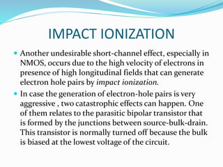
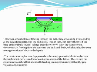
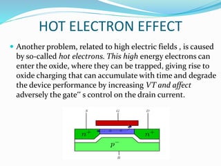
This document discusses short channel effects that occur in MOSFET devices when the channel length decreases to the same order of magnitude as the source/drain junction depth. It describes five main short channel effects: drain induced barrier lowering, drain punch through, velocity saturation, impact ionization, and hot electron effects. For each effect, it provides an explanation of the physical phenomenon and how it impacts device performance as the channel length decreases. It concludes by listing three references for further reading on leakage current mechanisms and MOSFET modeling.
Reduced channel length cause departures from long channel behaviour as two-dimensional potential distribution and high electric fields give birth to Short channel effects.
SHORT-CHANNEL EFFECTS
A MOSFET is considered to be short when the channel length ‘L’ is the same order of magnitude as the depletion-layer widths (xdD, xdS). The potential distribution in the channel now depends upon both, transverse field Ex, due to gate bias and also on the longitudinal field Ey, due to drain bias When the Gate channel length <<1 m, short channel effect becomes important .
This leads to many
undesirable effects in MOSFET.
The short-channel effects are attributed to two physical phenomena:
A) The limitation imposed on electron drift characteristics in the channel,
B) The modification of the threshold voltage due to the shortening channel length.
In particular five different short-channel effects can be distinguished:
1. Drain-induced barrier lowering and “Punch through”
2. Surface scattering
3. Velocity saturation
4. Impact ionization
5. Hot electrons
Here are the all short channel effects that you require.It consist of:-
Drain Induced Barrier Lowering
Hot electron Effect
Impact Ionization
Surface Scattering
Velocity saturation
Threshold Voltage & Channel Length ModulationBulbul Brahma
Design and Technology of Electronic Devices:
Review of microelectronic devices, introduction to MOS technology and related devices.
MOS transistor theory, scaling theory related to MOS circuits, short channel effect and its
consequences, narrow width effect, FN tunnelling, Double gate MOSFET, Cylindrical
MOSFET, Basic concept of CMOS circuits and logic design. Circuit characterization and
performance estimation, important issues in real devices. PE logic, Domino logic, Pseudo
N-MOS logic-dynamic CMOS and Clocking, layout design and stick diagram, CMOS
analog circuit design, CMOS design methods. Introduction to SOI, Multi layer circuit
design and 3D integration. CMOS processing technology: Crystal grown and Epitaxy, Film
formation, Lithography and Etching, Impurity doping, Integrated Devices.
A simple N-channel MOSFET can be used as a diode, Switch and Active resistor. This presentation is a part of course of Analog CMOS Design, based on textbook of same title by Allen Holberg.
Field Effect Transistor, JFET, Metal Oxide Semiconductor Field Effect Transistor, Depletion MOSFET, Enhancement MoSFET, Construction, Basic operation, Regions of Operation, Drain Characteristics, Transfer Characteristics, Biasing, Non-Ideal Characteristics of E-MOSFET, DC Analysis, AC equivalent circuit and Parameters, E-MOSFET as an Amplifier, AC analysis, MOSFET as a Switch, MOSFET as a diode, MOSFET as a resistor, High frequency equivalent circuit, Miller Capacitance, Frequency Response, NMOS and CMOS inverter
In MOS, source-drain regions of adjacent MOS transistors together with interconnection metal lines may constitute parasitic MOS transistors unless they are isolated from each other. Hence, each MOSFET must be electrically isolated from each other. Device Isolation Techniques in VLSI microfabrication of MOS are discussed.
In electronics, short-channel effects occur in MOSFETs in which the channel length is comparable to the depletion layer widths of the source and drain junctions. These effects include, in particular, drain-induced barrier lowering, velocity saturation, Quantum confinement and hot carrier degradation
Short Channel Effects are governed by complex physical phenomena and mainly Influenced because of both vertical and horizontal electric field components.
To meet the current requirements of
Electronic devices, the miniaturization of devices is important. And so is Second Order effects which otherwise degrade the performance of devices.
This fun and visually appealing presentation about the core concept of diodes formation and application is thoroughly researched and concise. It contains fun tit-bits of info that make the concept of depletion layer easy to understand. It has a vibrant color scheme to make a perfect first impression for any project...
Electrical stray current refers to the flow of electrical current via two objects due to potential difference, imbalance or wiring flaws. Small voltage difference between two grounded objects in separate location may exist because of ordinary flow of current within the power system. However, large voltage difference can be a sign of faulty condition in electrical power system. Visit (electricalride.com) for more related articles.
AES2013 Harnett plenary talk: Electrodes for microfluidic applicationsCK Harnett
Four ways to make metal 3D electrodes for microfluidics, without electroplating. The slides show examples from induced-charge electroosmosis and particle counting.
Quality defects in TMT Bars, Possible causes and Potential Solutions.PrashantGoswami42
Maintaining high-quality standards in the production of TMT bars is crucial for ensuring structural integrity in construction. Addressing common defects through careful monitoring, standardized processes, and advanced technology can significantly improve the quality of TMT bars. Continuous training and adherence to quality control measures will also play a pivotal role in minimizing these defects.
Vaccine management system project report documentation..pdfKamal Acharya
The Division of Vaccine and Immunization is facing increasing difficulty monitoring vaccines and other commodities distribution once they have been distributed from the national stores. With the introduction of new vaccines, more challenges have been anticipated with this additions posing serious threat to the already over strained vaccine supply chain system in Kenya.
NO1 Uk best vashikaran specialist in delhi vashikaran baba near me online vas...Amil Baba Dawood bangali
Contact with Dawood Bhai Just call on +92322-6382012 and we'll help you. We'll solve all your problems within 12 to 24 hours and with 101% guarantee and with astrology systematic. If you want to take any personal or professional advice then also you can call us on +92322-6382012 , ONLINE LOVE PROBLEM & Other all types of Daily Life Problem's.Then CALL or WHATSAPP us on +92322-6382012 and Get all these problems solutions here by Amil Baba DAWOOD BANGALI
#vashikaranspecialist #astrologer #palmistry #amliyaat #taweez #manpasandshadi #horoscope #spiritual #lovelife #lovespell #marriagespell#aamilbabainpakistan #amilbabainkarachi #powerfullblackmagicspell #kalajadumantarspecialist #realamilbaba #AmilbabainPakistan #astrologerincanada #astrologerindubai #lovespellsmaster #kalajaduspecialist #lovespellsthatwork #aamilbabainlahore#blackmagicformarriage #aamilbaba #kalajadu #kalailam #taweez #wazifaexpert #jadumantar #vashikaranspecialist #astrologer #palmistry #amliyaat #taweez #manpasandshadi #horoscope #spiritual #lovelife #lovespell #marriagespell#aamilbabainpakistan #amilbabainkarachi #powerfullblackmagicspell #kalajadumantarspecialist #realamilbaba #AmilbabainPakistan #astrologerincanada #astrologerindubai #lovespellsmaster #kalajaduspecialist #lovespellsthatwork #aamilbabainlahore #blackmagicforlove #blackmagicformarriage #aamilbaba #kalajadu #kalailam #taweez #wazifaexpert #jadumantar #vashikaranspecialist #astrologer #palmistry #amliyaat #taweez #manpasandshadi #horoscope #spiritual #lovelife #lovespell #marriagespell#aamilbabainpakistan #amilbabainkarachi #powerfullblackmagicspell #kalajadumantarspecialist #realamilbaba #AmilbabainPakistan #astrologerincanada #astrologerindubai #lovespellsmaster #kalajaduspecialist #lovespellsthatwork #aamilbabainlahore #Amilbabainuk #amilbabainspain #amilbabaindubai #Amilbabainnorway #amilbabainkrachi #amilbabainlahore #amilbabaingujranwalan #amilbabainislamabad
Cosmetic shop management system project report.pdfKamal Acharya
Buying new cosmetic products is difficult. It can even be scary for those who have sensitive skin and are prone to skin trouble. The information needed to alleviate this problem is on the back of each product, but it's thought to interpret those ingredient lists unless you have a background in chemistry.
Instead of buying and hoping for the best, we can use data science to help us predict which products may be good fits for us. It includes various function programs to do the above mentioned tasks.
Data file handling has been effectively used in the program.
The automated cosmetic shop management system should deal with the automation of general workflow and administration process of the shop. The main processes of the system focus on customer's request where the system is able to search the most appropriate products and deliver it to the customers. It should help the employees to quickly identify the list of cosmetic product that have reached the minimum quantity and also keep a track of expired date for each cosmetic product. It should help the employees to find the rack number in which the product is placed.It is also Faster and more efficient way.
CFD Simulation of By-pass Flow in a HRSG module by R&R Consult.pptxR&R Consult
CFD analysis is incredibly effective at solving mysteries and improving the performance of complex systems!
Here's a great example: At a large natural gas-fired power plant, where they use waste heat to generate steam and energy, they were puzzled that their boiler wasn't producing as much steam as expected.
R&R and Tetra Engineering Group Inc. were asked to solve the issue with reduced steam production.
An inspection had shown that a significant amount of hot flue gas was bypassing the boiler tubes, where the heat was supposed to be transferred.
R&R Consult conducted a CFD analysis, which revealed that 6.3% of the flue gas was bypassing the boiler tubes without transferring heat. The analysis also showed that the flue gas was instead being directed along the sides of the boiler and between the modules that were supposed to capture the heat. This was the cause of the reduced performance.
Based on our results, Tetra Engineering installed covering plates to reduce the bypass flow. This improved the boiler's performance and increased electricity production.
It is always satisfying when we can help solve complex challenges like this. Do your systems also need a check-up or optimization? Give us a call!
Work done in cooperation with James Malloy and David Moelling from Tetra Engineering.
More examples of our work https://www.r-r-consult.dk/en/cases-en/
Immunizing Image Classifiers Against Localized Adversary Attacksgerogepatton
This paper addresses the vulnerability of deep learning models, particularly convolutional neural networks
(CNN)s, to adversarial attacks and presents a proactive training technique designed to counter them. We
introduce a novel volumization algorithm, which transforms 2D images into 3D volumetric representations.
When combined with 3D convolution and deep curriculum learning optimization (CLO), itsignificantly improves
the immunity of models against localized universal attacks by up to 40%. We evaluate our proposed approach
using contemporary CNN architectures and the modified Canadian Institute for Advanced Research (CIFAR-10
and CIFAR-100) and ImageNet Large Scale Visual Recognition Challenge (ILSVRC12) datasets, showcasing
accuracy improvements over previous techniques. The results indicate that the combination of the volumetric
input and curriculum learning holds significant promise for mitigating adversarial attacks without necessitating
adversary training.
Saudi Arabia stands as a titan in the global energy landscape, renowned for its abundant oil and gas resources. It's the largest exporter of petroleum and holds some of the world's most significant reserves. Let's delve into the top 10 oil and gas projects shaping Saudi Arabia's energy future in 2024.
Industrial Training at Shahjalal Fertilizer Company Limited (SFCL)MdTanvirMahtab2
This presentation is about the working procedure of Shahjalal Fertilizer Company Limited (SFCL). A Govt. owned Company of Bangladesh Chemical Industries Corporation under Ministry of Industries.
Democratizing Fuzzing at Scale by Abhishek Aryaabh.arya
Presented at NUS: Fuzzing and Software Security Summer School 2024
This keynote talks about the democratization of fuzzing at scale, highlighting the collaboration between open source communities, academia, and industry to advance the field of fuzzing. It delves into the history of fuzzing, the development of scalable fuzzing platforms, and the empowerment of community-driven research. The talk will further discuss recent advancements leveraging AI/ML and offer insights into the future evolution of the fuzzing landscape.
Hybrid optimization of pumped hydro system and solar- Engr. Abdul-Azeez.pdffxintegritypublishin
Advancements in technology unveil a myriad of electrical and electronic breakthroughs geared towards efficiently harnessing limited resources to meet human energy demands. The optimization of hybrid solar PV panels and pumped hydro energy supply systems plays a pivotal role in utilizing natural resources effectively. This initiative not only benefits humanity but also fosters environmental sustainability. The study investigated the design optimization of these hybrid systems, focusing on understanding solar radiation patterns, identifying geographical influences on solar radiation, formulating a mathematical model for system optimization, and determining the optimal configuration of PV panels and pumped hydro storage. Through a comparative analysis approach and eight weeks of data collection, the study addressed key research questions related to solar radiation patterns and optimal system design. The findings highlighted regions with heightened solar radiation levels, showcasing substantial potential for power generation and emphasizing the system's efficiency. Optimizing system design significantly boosted power generation, promoted renewable energy utilization, and enhanced energy storage capacity. The study underscored the benefits of optimizing hybrid solar PV panels and pumped hydro energy supply systems for sustainable energy usage. Optimizing the design of solar PV panels and pumped hydro energy supply systems as examined across diverse climatic conditions in a developing country, not only enhances power generation but also improves the integration of renewable energy sources and boosts energy storage capacities, particularly beneficial for less economically prosperous regions. Additionally, the study provides valuable insights for advancing energy research in economically viable areas. Recommendations included conducting site-specific assessments, utilizing advanced modeling tools, implementing regular maintenance protocols, and enhancing communication among system components.
2. CONTENTS
SHORT CHANNEL DEVICE
SHORT CHANNEL EFFECTS:
DRAIN INDUCED BARRIER LOWERING
DRAIN PUNCH THROUGH
VELOCITY SATURATION
IMPACT IONIZATION
HOT ELECTRON EFFECT
REFERENCES
3. SHORT CHANNEL DEVICE
When the channel of the MOSFET becomes the
same order of magnitude as the junction depth of
source and drain, the device is said to be a short
channel device.
The short-channel effects are attributed to two
physical phenomena:
A) The limitation imposed on electron drift
characteristics in the channel,
B) The modification of the threshold voltage due to
the shortening channel length.
4. SHORT CHANNEL EFFECTS
1. Drain-induced barrier lowering
2. Drain Punch Through
3. Velocity saturation
4. Impact ionization
5. Hot electrons
5. DRAIN INDUCED BARRIER LOWERING
Under normal conditions (VDS=0 and VGS=0), there is a
potential barrier that stops the electrons from flowing from
source to drain. The gate voltage has the function of
lowering this barrier down to the point where electrons are
able to flow . Ideally, this would be the only voltage that
would affect the barrier. However, as the channel becomes
shorter, a larger VD widens the drain depletion region to a
point that reduces the potential barrier . For this reason,
this effect is aptly called Drain Induced Barrier
Lowering (DIBL).
6. DRAIN PUNCH THROUGH
When the drain is at high enough voltage with
respect to the source, the depletion region around
the drain may extend to the source, causing current
to flow irrespective of gate voltage (i.e. even if gate
voltage is zero). This is known as Drain Punch
Through condition .
So when channel length L decreases (i.e. short
channel length case), punch through voltage rapidly
decreases.
7. VELOCITY SATURATION
The performance short-channel devices is also affected
by velocity saturation.
At low Ey, the electron drift velocity Vde in the channel
varies linearly with the electric field intensity.
However, as Ey increases the drift velocity tends to
increase more slowly, and approaches a saturation
value.
The drain current is limited by velocity saturation
instead of pinch off.
8. IMPACT IONIZATION
Another undesirable short-channel effect, especially in
NMOS, occurs due to the high velocity of electrons in
presence of high longitudinal fields that can generate
electron hole pairs by impact ionization.
In case the generation of electron-hole pairs is very
aggressive , two catastrophic effects can happen. One
of them relates to the parasitic bipolar transistor that
is formed by the junctions between source-bulk-drain.
This transistor is normally turned off because the bulk
is biased at the lowest voltage of the circuit.
9. • However, when holes are flowing through the bulk, they are causing a voltage drop
at the parasitic resistance of the bulk itself. This, in turn, can active the BJT if the
base-emitter (bulk-source) voltage exceeds 0.6-0.7 V. With the transistor on,
electrons start flowing from the source to the bulk and drain, which can lead to even
more generation of electron-hole pairs.
•The most catastrophic case happens when the newly generated electrons become
themselves hot carriers and knock out other atoms of the lattice. This in turn can
create an avalanche effect, eventually leading to an overrun current that the gate
voltage cannot control.
10. HOT ELECTRON EFFECT
Another problem, related to high electric fields , is caused
by so-called hot electrons. This high energy electrons can
enter the oxide, where they can be trapped, giving rise to
oxide charging that can accumulate with time and degrade
the device performance by increasing VT and affect
adversely the gate‟ s control on the drain current.
11. REFERENCES
[1] Kaushi Roy, Saibal Mukhopadhyay and Hamid
Mahmoodi-Meimand, "Leakage current mechanisms
and leakage reduction techniques in deep-
submicrometer CMOS circuits", Proceedings of the
IEEE, 305-327, vol. 91, no.2, February 2003.
[2].Sung-Mo Kang and Yusuf Leblebici, Cmos Digital
Integrated Circuits, Tata McGraw-Hill Education,
2003.
[3]. Narain Arora, Mosfet Modeling for VLSI Simulation:
Theory and Practice, WORLD SCIENTIFIC, 2007