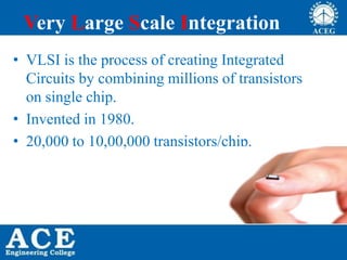
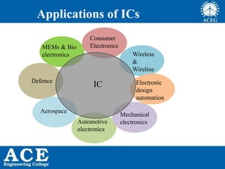
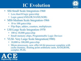
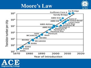
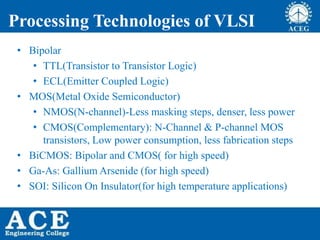
1
UNIT-1
Introduction to IC Technology
2
•Introduction to IC Technology
•What is VLSI?
•Why VLSI?
•Applications of ICs
•IC Evolution
•Moore’s law
•Processing Technologies
Contents
3
Guess the Device?
5MB Hard disk by IBM in 1956
Advancement due to VLSI
5MB(IBM)-1956, $10,000/MB 1TB(Samsung)-2020, 200$/TB
Achieved through VLSI
ENIAC-Worlds first electronic computer(1946) Computer in 2020
Very Large Scale Integration
• VLSI is the process of creating Integrated
Circuits by combining millions of transistors
on single chip.
• Invented in 1980.
• 20,000 to 10,00,000 transistors/chip.
Why VLSI?
• Physical size of device can be reduced
• Effective cost of the devices can be reduced
• The operating speed of circuit is increased
• Requires less power
• Higher reliability
• Easier to design
Applications of ICs
Consumer
Electronics
Wireless
&
Wireline
Electronic
design
automation
Mechanical
electronicsAutomotive
electronics
Aerospace
Defence
MEMs & Bio
electronics
IC
IC Evolution
• SSI-Small Scale Integration-1960
• Less than10 logic gates/chip
• Logic gates(AND,OR,NAND,NOR)
• MSI-Medium Scale Integration-1966
• 10 to 100 gates/chip
• Flip flops, adders, counters, multiplexers
• LSI-Large Scale Integration-1970
• 100 to 10,000 gates/chip
• Small memory chips, Programmable Logic Devices
• VLSI- Very Large Scale Integration(1980)
• 10,000 to 100,000 gates/chip
• Micro processors, now offer 64-bit processor complete with
cache memory, floating point arithmetic units, RAM,ROM,
complex PLDs.
Moore’s Law
Moore’s Law contd..
• The number of transistors on an integrated circuit will
double every 18 months
• In 1965, Gordon Moore, co founder of Intel, predicted
that the number of transistors that can be integrated on
a die would double every 18 to 14 months
• i.e., grow exponentially with time
• 2300 transistors, 1 MHz clock (Intel 4004) – 1971
• 2.16 Billion transistors,126sq.mm, 2.9GHz (Intel
i7) -2009
Processing Technologies of VLSI
• Bipolar
• TTL(Transistor to Transistor Logic)
• ECL(Emitter Coupled Logic)
• MOS(Metal Oxide Semiconductor)
• NMOS(N-channel)-Less masking steps, denser, less power
• CMOS(Complementary): N-Channel & P-channel MOS
transistors, Low power consumption, less fabrication steps
• BiCMOS: Bipolar and CMOS( for high speed)
• Ga-As: Gallium Arsenide (for high speed)
• SOI: Silicon On Insulator(for high temperature applications)
13
Power dissipation & Propagation delay
Processing Technologies Overview
CMOS:90%
BICMOS:5%
BIPOLAR:2%
GaAs:2%
SOI:1%
NMOS & PMOS transistors
2002: L=130nm
2003:L=90nm
2019:L=7nm
2020:L=5nm?

VLSI Design-Lecture2 introduction to ic technology

  • 1.
  • 2.
    2 •Introduction to ICTechnology •What is VLSI? •Why VLSI? •Applications of ICs •IC Evolution •Moore’s law •Processing Technologies Contents
  • 3.
    3 Guess the Device? 5MBHard disk by IBM in 1956
  • 4.
    Advancement due toVLSI 5MB(IBM)-1956, $10,000/MB 1TB(Samsung)-2020, 200$/TB
  • 5.
    Achieved through VLSI ENIAC-Worldsfirst electronic computer(1946) Computer in 2020
  • 6.
    Very Large ScaleIntegration • VLSI is the process of creating Integrated Circuits by combining millions of transistors on single chip. • Invented in 1980. • 20,000 to 10,00,000 transistors/chip.
  • 7.
    Why VLSI? • Physicalsize of device can be reduced • Effective cost of the devices can be reduced • The operating speed of circuit is increased • Requires less power • Higher reliability • Easier to design
  • 8.
  • 9.
    IC Evolution • SSI-SmallScale Integration-1960 • Less than10 logic gates/chip • Logic gates(AND,OR,NAND,NOR) • MSI-Medium Scale Integration-1966 • 10 to 100 gates/chip • Flip flops, adders, counters, multiplexers • LSI-Large Scale Integration-1970 • 100 to 10,000 gates/chip • Small memory chips, Programmable Logic Devices • VLSI- Very Large Scale Integration(1980) • 10,000 to 100,000 gates/chip • Micro processors, now offer 64-bit processor complete with cache memory, floating point arithmetic units, RAM,ROM, complex PLDs.
  • 10.
  • 11.
    Moore’s Law contd.. •The number of transistors on an integrated circuit will double every 18 months • In 1965, Gordon Moore, co founder of Intel, predicted that the number of transistors that can be integrated on a die would double every 18 to 14 months • i.e., grow exponentially with time • 2300 transistors, 1 MHz clock (Intel 4004) – 1971 • 2.16 Billion transistors,126sq.mm, 2.9GHz (Intel i7) -2009
  • 12.
    Processing Technologies ofVLSI • Bipolar • TTL(Transistor to Transistor Logic) • ECL(Emitter Coupled Logic) • MOS(Metal Oxide Semiconductor) • NMOS(N-channel)-Less masking steps, denser, less power • CMOS(Complementary): N-Channel & P-channel MOS transistors, Low power consumption, less fabrication steps • BiCMOS: Bipolar and CMOS( for high speed) • Ga-As: Gallium Arsenide (for high speed) • SOI: Silicon On Insulator(for high temperature applications)
  • 13.
    13 Power dissipation &Propagation delay
  • 14.
  • 15.
    NMOS & PMOStransistors 2002: L=130nm 2003:L=90nm 2019:L=7nm 2020:L=5nm?