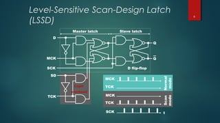
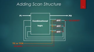
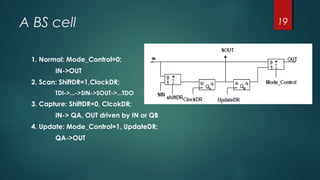
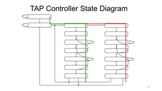
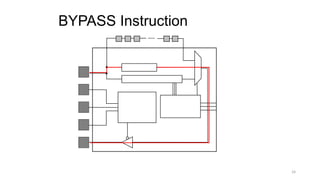
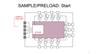
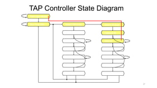
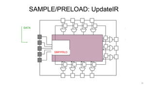
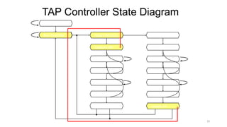
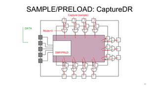
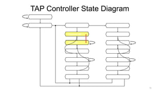
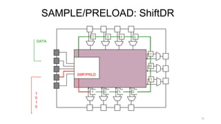
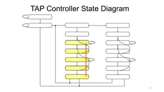
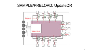
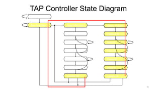
Level sensitive scan
design
PRESENTED BY,
PRAVEENKUMAR S – 15E137
1
Design for testability
 Design for testability (DFT) refers to the design techniques
that make test generation and test application cost-
effective.
 DFT methods for digital circuits:
 Ad-hoc methods
 Structured methods:
 Scan
 Partial Scan
 Boundary scan
2
Scan chain
 Circuit is designed using pre-specified design rules.
 Test structure (hardware) is added to the verified design:
 Replacing flip-flops by scan flip-flops and connect to form one or more
shift registers in the test mode.
 Make input/output of each scan shift register controllable/observable
from PI/PO.
 Scan design techniques involves modifying the registers to allow them to be
chained into a long shift register, called a scan chain.
3
Scan Flip-Flop (master-slave) 4
D
TC
SD
CK
Q
Q
MUX
D flip-flop
Master latch Slave latch
CK
TC Normal mode, D selected Scan mode, SD selected
Master open Slave open
t
t
Logic
overhead
Operation
 Circuit with two modes of operation
 Normal functional mode
 Test mode
 Circuit bistables are interconnected into a shift register With the circuit in test
mode It is possible to shift an arbitrary test pattern into the bistables.
 By returning the circuit to normal mode for one clock period the
combinational circuitry acts upon the bistable contents and primary input
signals, Stores the results in the bistables Circuit is then placed into test mode
 It is possible to shift out the contents of the bistables and compare these
contents with the correct response
5
Level-Sensitive Scan-Design Latch
(LSSD)
6
D
SD
MCK
Q
Q
D flip-flop
Master latch Slave latch
t
SCK
TCK
SCK
MCK
TCK
Normal
mode
MCK
TCK
Scan
mode
Logic
overhead
Adding Scan Structure 7
SFF
SFF
SFF
Combinational
logic
PI PO
SCANOUT
SCANIN
TC or TCK
Comb. Test Vectors 8
I2I1
O1 O2
PI
PO
SCANIN
SCANOUT
S1 S2
N1 N2
0 0 0 0 0 0 0 1 0 0 0 0 0 0 0 1 0 0 0 0 0 0 0TC
Don’t care
or random
bits
Sequence length = (nsff + 1) ncomb + nsff clock periods
ncomb = number of combinational vectors
nsff = number of scan flip-flops
Multiple Scan Registers
 Scan flip-flops can be distributed among
any number of shift registers, each having
a separate scanin and scanout pin.
 Test sequence length is determined by
the longest scan shift register.
9
SFF
SFF
SFF
Combinational
logic
PI/SCANIN PO/
SCANOUTM
U
X
CK
TC
Hierarchical Scan
 Scan flip-flops are chained within
subnetworks before chaining subnetworks.
 Advantages:
 Automatic scan insertion in netlist
 Circuit hierarchy preserved – helps in debugging and
design changes
 Disadvantage: Non-optimum chip layout.
10
SFF1
SFF2 SFF3
SFF4
SFF3SFF1
SFF2SFF4
Scanin Scanout
Scanin
Scanout
Hierarchical netlist Flat layout
Cons.
 If the path is a critical timing path, performance of the whole system is
affected.
 Another disadvantage of scan design, when compared to some other DFT
techniques, is that the scan chain is very long.
 Shifting test vectors in and result vectors out takes a large fraction of test time,
so the system cannot be tested at full operational speed.
11
Level-Sensitive Scan Design (LSSD)
 This approach was introduced by Eichelberger and T. Williams in 1977 and 1978.
It is a latch-based design used at IBM.
 It guarantees race-free and hazard-free system operation as well as testing.
 Level-sensitive scan design (LSSD) is part of an integrated circuit manufacturing
test process.
 It is a DFT scan design method which uses separate system and scan clocks to
distinguish between normal and test mode.
 Latches are used in pairs, each has a normal data input, data output and clock
for system operation. For test operation, the two latches form a master/slave
pair with one scan input, one scan output and non-overlapping scan clocks A
and B which are held low during system operation but cause the scan data to
be latched when pulsed high during scan.
12
Advantages & Drawbacks of LSSD
1. Correct operation independent of AC characteristics is guaranteed.
2. FSM is reduced to combinational logic as far as testing is concerned.
3. Hazards and races are eliminated, which simplifies test generation and fault
simulation.
1. Complex design rules are imposed on designers.
2. Asynchronous designs are not allowed in this approach.
3. Sequential routing of latches can introduce irregular structures.
4. Faults changing combinational function to sequential one may cause trouble, e.g.,
bridging and CMOS stuck-open faults.
5. Test application becomes a slow process, and normal-speed testing of the entire test
sequence is impossible.
6. It is not good for memory intensive designs.
13
Boundary scan test
14
Boundary scan
 Boundary scan is a method for testing interconnects (wire lines) on printed circuit
boards or sub-blocks inside an integrated circuit. Boundary scan is also widely used
as a debugging method to watch integrated circuit pin states, measure voltage, or
analyze sub-blocks inside an integrated circuit.
 The success of boundary scan techniques led to the formation of the Joint Test
Action Group (JTAG) in the 1980s for standardizing boundary scan components and
protocols.
 Each component have a test access port (TAP), consisting of the following
connections:
o Test Clock (TCK): provides the clock signal for the test logic.
o Test Mode Select Input (TMS): controls test operation.
o Test Data Input (TDI): serial input for test data and instructions.
o Test Data Output (TDO): serial output for test data and instructions.
15
16
Boundary Scan Test Logic 17
Operation
 To test the PCB, the test equipment shifts a test vector into the scan chain.
When the chain is loaded, the vector is driven onto the external outputs of the
chips.
 The scan-chain flip-flops then sample the external inputs, and the sampled
values are shifted out to the test equipment.
 The test equipment can then verify that all of the connections between the
chips.
 The TAP Controller operates as a simple finite-state machine, changing between
states depending on the value of the TMS input. Different states govern shifting
of data into the Instruction Register or one of the data registers.
 The JTAG standard defines a number of instructions formats for operations that
select among data registers, control the mode of the scan chain
18
A BS cell 19
1. Normal: Mode_Control=0;
IN->OUT
2. Scan: ShiftDR=1,ClockDR;
TDI->...->SIN->SOUT->...TDO
3. Capture: ShiftDR=0, ClcokDR;
IN-> QA, OUT driven by IN or QB
4. Update: Mode_Control=1, UpdateDR;
QA->OUT
TAP Controller State Diagram
20
Select-DR-Scan
Capture-DR
Shift-DR
Exit1-DR
Pause-DR
Exit2-DR
Update-DR
0
0
1
0
1
1
Test-Logic-Reset
Run-Test/Idle
0
1
0
1
0
1
0
0
Select-IR-Scan
Capture-IR
Shift-IR
Exit1-IR
Pause-IR
Exit2-IR
Update-IR
0
0
1
0
1
1
1
0
1
0
0
0101
States of TAP Controller
 Test-Logic-Reset: normal mode
 Run-Test/Idle: wait for internal test
 Select-DR-Scan: initiate a data-scan sequence
 Capture-DR: load test data in parallel
 Shift-DR: load test data in series
 Exit1-DR: finish phase-1 shifting of data
 Pause-DR: temporarily hold the scan operation (allow the bus master to reload
data)
 Exit2-DR: finish phase-2 shifting of data
 Update-DR: parallel load from associated shift registers
21
BSDL
 BSDL description of a component, together with a set of test vectors, as input to
ATE for testing the component and the board in which it is embedded.
 Test data can be shifted into the cells at the inputs and then driven onto the
core’s inputs. The core’s outputs can be sampled into the cells at the output
pins and then shifted out to the ATE.
 Thus, the JTAG architecture solves two problems: in-circuit testing of
components in a system, and in-circuit testing of the connections between the
components.
22
Boundary Scan
Instructions
23
BYPASS Instruction
24
TDI
TMS
TCK
TRST_N
TDO
Finite
State
Machine
Instruction Register
Instruction
Decode
SOSI
Bypass Reg. Bypasses scan chain with
1-bit register
Usually loaded in chips
that are idle while other
chips on the board are
being tested
EXTEST & SAMPLE/PRELOAD
• Test off-chip circuits and board-level
interconnections
• Data is first loaded into boundary register chain
with SAMPLE/PRELOAD instruction
• Samples inputs and outputs, pass-through
• Loads boundary register with data
25
SAMPLE/PRELOAD: Start
26
SAMPLE/
PRELOAD
Chip
Core
TAP
Controller
TDI
TMS
TCK
TDO
TRST_N
BYPASS
TAP Controller State Diagram
Select-DR-Scan
Capture-DR
Shift-DR
Exit1-DR
Pause-DR
Exit2-DR
Update-DR
0
0
1
0
1
1
Test-Logic-Reset
Run-Test/Idle
0
1
0
1
0
1
0
0
Select-IR-Scan
Capture-IR
Shift-IR
Exit1-IR
Pause-IR
Exit2-IR
Update-IR
0
0
1
0
1
1
1
0
1
0
0
0101
27
SAMPLE/PRELOAD: UpdateIR
28
SAMPLE/
PRELOAD
Chip
Core
TAP
Controller
TDI
TMS
TCK
TDO
TRST_N
BYPASSSMP/PRLD
DATA 1.Get snapshot of
normal chip output
signals
2.Put data on bound.
scan chain before next
instr.
Update-DR
Exit2-DR
Pause-DR
Exit1-DR
Shift-DR
Exit2-IR
Pause-IR
Exit1-IR
Shift-IR
Capture-IR
TAP Controller State Diagram
Select-DR-Scan
Capture-DR
0
0
1
0
1
1
Test-Logic-Reset
Run-Test/Idle
0
1
0
1
0
1
0
0
Select-IR-Scan
0
0
1
0
1
1
1
0
1
0
0
0101
Update-IR
29
SAMPLE/PRELOAD: CaptureDR
30
Chip
Core
TAP
Controller
TDI
TMS
TCK
TDO
TRST_N
SMP/PRLD
DATA
Mode=0
Capture (sample)
0 1 0 1
0 1 0 1
0
1
0
Update-DR
Exit2-DR
Pause-DR
Exit1-DR
Shift-DR
Update-IR
Exit2-IR
Pause-IR
Exit1-IR
Shift-IR
Capture-IR
TAP Controller State Diagram
Select-DR-Scan
Capture-DR
0
0
1
0
1
1
Test-Logic-Reset
Run-Test/Idle
0
1
0
1
0
1
0
0
Select-IR-Scan
0
0
1
0
1
1
1
0
1
0
0
0101
31
SAMPLE/PRELOAD: ShiftDR
32
Chip
Core
TAP
Controller
TDI
TMS
TCK
TDO
TRST_N
SMP/PRLD
DATA
0 1 0 11 0 1 0
0 1 0 1
1
0
0
01011
0
1
0
0
1
1
Update-IR
Exit2-IR
Pause-IR
Exit1-IR
Shift-IR
Capture-IR
TAP Controller State Diagram
Select-DR-Scan
Capture-DR
Shift-DR
Exit1-DR
Pause-DR
Exit2-DR
Update-DR
0
0
1
0
1
1
Test-Logic-Reset
Run-Test/Idle
0
1
0
1
0
1
0
0
Select-IR-Scan
0
0
1
0
1
1
1
0
1
0
0
0101
33
SAMPLE/PRELOAD: UpdateDR
34
Chip
Core
TAP
Controller
TDI
TMS
TCK
TDO
TRST_N
SMP/PRLD
1 0 1 0
0101
0
1
1
Mode=0
TAP Controller State Diagram
Select-DR-Scan
Capture-DR
Shift-DR
Exit1-DR
Pause-DR
Exit2-DR
0
0
1
0
1
1
Test-Logic-Reset
Run-Test/Idle
0
1
0
1
0
1
0
0
Select-IR-Scan
Capture-IR
Shift-IR
Exit1-IR
Pause-IR
Exit2-IR
Update-IR
0
0
1
0
1
1
1
0
1
0
0
0101
Update-DR
35
References
 Lecture ppt on : Intro to boundary scan by David lavo
 Peter J. Ashenden-Digital Design
36
Thank you
37

Level sensitive scan design(LSSD) and Boundry scan(BS)

  • 1.
    Level sensitive scan design PRESENTEDBY, PRAVEENKUMAR S – 15E137 1
  • 2.
    Design for testability Design for testability (DFT) refers to the design techniques that make test generation and test application cost- effective.  DFT methods for digital circuits:  Ad-hoc methods  Structured methods:  Scan  Partial Scan  Boundary scan 2
  • 3.
    Scan chain  Circuitis designed using pre-specified design rules.  Test structure (hardware) is added to the verified design:  Replacing flip-flops by scan flip-flops and connect to form one or more shift registers in the test mode.  Make input/output of each scan shift register controllable/observable from PI/PO.  Scan design techniques involves modifying the registers to allow them to be chained into a long shift register, called a scan chain. 3
  • 4.
    Scan Flip-Flop (master-slave)4 D TC SD CK Q Q MUX D flip-flop Master latch Slave latch CK TC Normal mode, D selected Scan mode, SD selected Master open Slave open t t Logic overhead
  • 5.
    Operation  Circuit withtwo modes of operation  Normal functional mode  Test mode  Circuit bistables are interconnected into a shift register With the circuit in test mode It is possible to shift an arbitrary test pattern into the bistables.  By returning the circuit to normal mode for one clock period the combinational circuitry acts upon the bistable contents and primary input signals, Stores the results in the bistables Circuit is then placed into test mode  It is possible to shift out the contents of the bistables and compare these contents with the correct response 5
  • 6.
    Level-Sensitive Scan-Design Latch (LSSD) 6 D SD MCK Q Q Dflip-flop Master latch Slave latch t SCK TCK SCK MCK TCK Normal mode MCK TCK Scan mode Logic overhead
  • 7.
    Adding Scan Structure7 SFF SFF SFF Combinational logic PI PO SCANOUT SCANIN TC or TCK
  • 8.
    Comb. Test Vectors8 I2I1 O1 O2 PI PO SCANIN SCANOUT S1 S2 N1 N2 0 0 0 0 0 0 0 1 0 0 0 0 0 0 0 1 0 0 0 0 0 0 0TC Don’t care or random bits Sequence length = (nsff + 1) ncomb + nsff clock periods ncomb = number of combinational vectors nsff = number of scan flip-flops
  • 9.
    Multiple Scan Registers Scan flip-flops can be distributed among any number of shift registers, each having a separate scanin and scanout pin.  Test sequence length is determined by the longest scan shift register. 9 SFF SFF SFF Combinational logic PI/SCANIN PO/ SCANOUTM U X CK TC
  • 10.
    Hierarchical Scan  Scanflip-flops are chained within subnetworks before chaining subnetworks.  Advantages:  Automatic scan insertion in netlist  Circuit hierarchy preserved – helps in debugging and design changes  Disadvantage: Non-optimum chip layout. 10 SFF1 SFF2 SFF3 SFF4 SFF3SFF1 SFF2SFF4 Scanin Scanout Scanin Scanout Hierarchical netlist Flat layout
  • 11.
    Cons.  If thepath is a critical timing path, performance of the whole system is affected.  Another disadvantage of scan design, when compared to some other DFT techniques, is that the scan chain is very long.  Shifting test vectors in and result vectors out takes a large fraction of test time, so the system cannot be tested at full operational speed. 11
  • 12.
    Level-Sensitive Scan Design(LSSD)  This approach was introduced by Eichelberger and T. Williams in 1977 and 1978. It is a latch-based design used at IBM.  It guarantees race-free and hazard-free system operation as well as testing.  Level-sensitive scan design (LSSD) is part of an integrated circuit manufacturing test process.  It is a DFT scan design method which uses separate system and scan clocks to distinguish between normal and test mode.  Latches are used in pairs, each has a normal data input, data output and clock for system operation. For test operation, the two latches form a master/slave pair with one scan input, one scan output and non-overlapping scan clocks A and B which are held low during system operation but cause the scan data to be latched when pulsed high during scan. 12
  • 13.
    Advantages & Drawbacksof LSSD 1. Correct operation independent of AC characteristics is guaranteed. 2. FSM is reduced to combinational logic as far as testing is concerned. 3. Hazards and races are eliminated, which simplifies test generation and fault simulation. 1. Complex design rules are imposed on designers. 2. Asynchronous designs are not allowed in this approach. 3. Sequential routing of latches can introduce irregular structures. 4. Faults changing combinational function to sequential one may cause trouble, e.g., bridging and CMOS stuck-open faults. 5. Test application becomes a slow process, and normal-speed testing of the entire test sequence is impossible. 6. It is not good for memory intensive designs. 13
  • 14.
  • 15.
    Boundary scan  Boundaryscan is a method for testing interconnects (wire lines) on printed circuit boards or sub-blocks inside an integrated circuit. Boundary scan is also widely used as a debugging method to watch integrated circuit pin states, measure voltage, or analyze sub-blocks inside an integrated circuit.  The success of boundary scan techniques led to the formation of the Joint Test Action Group (JTAG) in the 1980s for standardizing boundary scan components and protocols.  Each component have a test access port (TAP), consisting of the following connections: o Test Clock (TCK): provides the clock signal for the test logic. o Test Mode Select Input (TMS): controls test operation. o Test Data Input (TDI): serial input for test data and instructions. o Test Data Output (TDO): serial output for test data and instructions. 15
  • 16.
  • 17.
  • 18.
    Operation  To testthe PCB, the test equipment shifts a test vector into the scan chain. When the chain is loaded, the vector is driven onto the external outputs of the chips.  The scan-chain flip-flops then sample the external inputs, and the sampled values are shifted out to the test equipment.  The test equipment can then verify that all of the connections between the chips.  The TAP Controller operates as a simple finite-state machine, changing between states depending on the value of the TMS input. Different states govern shifting of data into the Instruction Register or one of the data registers.  The JTAG standard defines a number of instructions formats for operations that select among data registers, control the mode of the scan chain 18
  • 19.
    A BS cell19 1. Normal: Mode_Control=0; IN->OUT 2. Scan: ShiftDR=1,ClockDR; TDI->...->SIN->SOUT->...TDO 3. Capture: ShiftDR=0, ClcokDR; IN-> QA, OUT driven by IN or QB 4. Update: Mode_Control=1, UpdateDR; QA->OUT
  • 20.
    TAP Controller StateDiagram 20 Select-DR-Scan Capture-DR Shift-DR Exit1-DR Pause-DR Exit2-DR Update-DR 0 0 1 0 1 1 Test-Logic-Reset Run-Test/Idle 0 1 0 1 0 1 0 0 Select-IR-Scan Capture-IR Shift-IR Exit1-IR Pause-IR Exit2-IR Update-IR 0 0 1 0 1 1 1 0 1 0 0 0101
  • 21.
    States of TAPController  Test-Logic-Reset: normal mode  Run-Test/Idle: wait for internal test  Select-DR-Scan: initiate a data-scan sequence  Capture-DR: load test data in parallel  Shift-DR: load test data in series  Exit1-DR: finish phase-1 shifting of data  Pause-DR: temporarily hold the scan operation (allow the bus master to reload data)  Exit2-DR: finish phase-2 shifting of data  Update-DR: parallel load from associated shift registers 21
  • 22.
    BSDL  BSDL descriptionof a component, together with a set of test vectors, as input to ATE for testing the component and the board in which it is embedded.  Test data can be shifted into the cells at the inputs and then driven onto the core’s inputs. The core’s outputs can be sampled into the cells at the output pins and then shifted out to the ATE.  Thus, the JTAG architecture solves two problems: in-circuit testing of components in a system, and in-circuit testing of the connections between the components. 22
  • 23.
  • 24.
    BYPASS Instruction 24 TDI TMS TCK TRST_N TDO Finite State Machine Instruction Register Instruction Decode SOSI BypassReg. Bypasses scan chain with 1-bit register Usually loaded in chips that are idle while other chips on the board are being tested
  • 25.
    EXTEST & SAMPLE/PRELOAD •Test off-chip circuits and board-level interconnections • Data is first loaded into boundary register chain with SAMPLE/PRELOAD instruction • Samples inputs and outputs, pass-through • Loads boundary register with data 25
  • 26.
  • 27.
    TAP Controller StateDiagram Select-DR-Scan Capture-DR Shift-DR Exit1-DR Pause-DR Exit2-DR Update-DR 0 0 1 0 1 1 Test-Logic-Reset Run-Test/Idle 0 1 0 1 0 1 0 0 Select-IR-Scan Capture-IR Shift-IR Exit1-IR Pause-IR Exit2-IR Update-IR 0 0 1 0 1 1 1 0 1 0 0 0101 27
  • 28.
    SAMPLE/PRELOAD: UpdateIR 28 SAMPLE/ PRELOAD Chip Core TAP Controller TDI TMS TCK TDO TRST_N BYPASSSMP/PRLD DATA 1.Getsnapshot of normal chip output signals 2.Put data on bound. scan chain before next instr.
  • 29.
    Update-DR Exit2-DR Pause-DR Exit1-DR Shift-DR Exit2-IR Pause-IR Exit1-IR Shift-IR Capture-IR TAP Controller StateDiagram Select-DR-Scan Capture-DR 0 0 1 0 1 1 Test-Logic-Reset Run-Test/Idle 0 1 0 1 0 1 0 0 Select-IR-Scan 0 0 1 0 1 1 1 0 1 0 0 0101 Update-IR 29
  • 30.
  • 31.
    Update-DR Exit2-DR Pause-DR Exit1-DR Shift-DR Update-IR Exit2-IR Pause-IR Exit1-IR Shift-IR Capture-IR TAP Controller StateDiagram Select-DR-Scan Capture-DR 0 0 1 0 1 1 Test-Logic-Reset Run-Test/Idle 0 1 0 1 0 1 0 0 Select-IR-Scan 0 0 1 0 1 1 1 0 1 0 0 0101 31
  • 32.
  • 33.
    Update-IR Exit2-IR Pause-IR Exit1-IR Shift-IR Capture-IR TAP Controller StateDiagram Select-DR-Scan Capture-DR Shift-DR Exit1-DR Pause-DR Exit2-DR Update-DR 0 0 1 0 1 1 Test-Logic-Reset Run-Test/Idle 0 1 0 1 0 1 0 0 Select-IR-Scan 0 0 1 0 1 1 1 0 1 0 0 0101 33
  • 34.
  • 35.
    TAP Controller StateDiagram Select-DR-Scan Capture-DR Shift-DR Exit1-DR Pause-DR Exit2-DR 0 0 1 0 1 1 Test-Logic-Reset Run-Test/Idle 0 1 0 1 0 1 0 0 Select-IR-Scan Capture-IR Shift-IR Exit1-IR Pause-IR Exit2-IR Update-IR 0 0 1 0 1 1 1 0 1 0 0 0101 Update-DR 35
  • 36.
    References  Lecture ppton : Intro to boundary scan by David lavo  Peter J. Ashenden-Digital Design 36
  • 37.