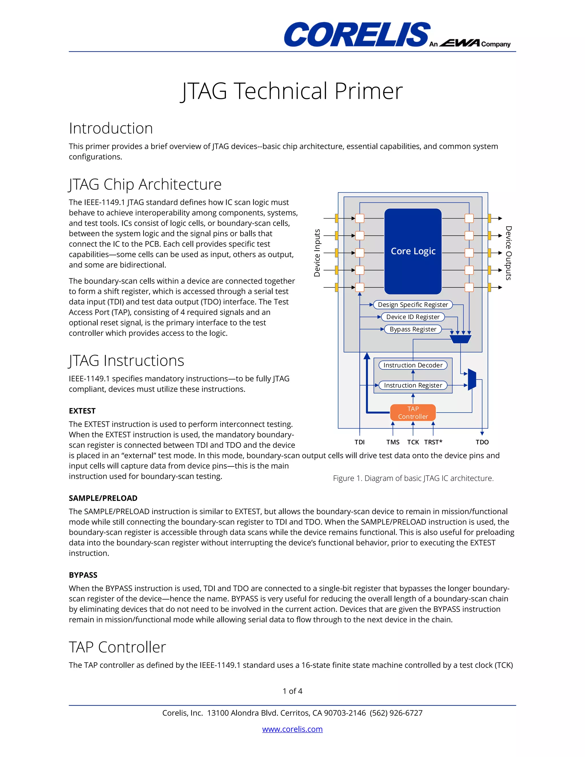
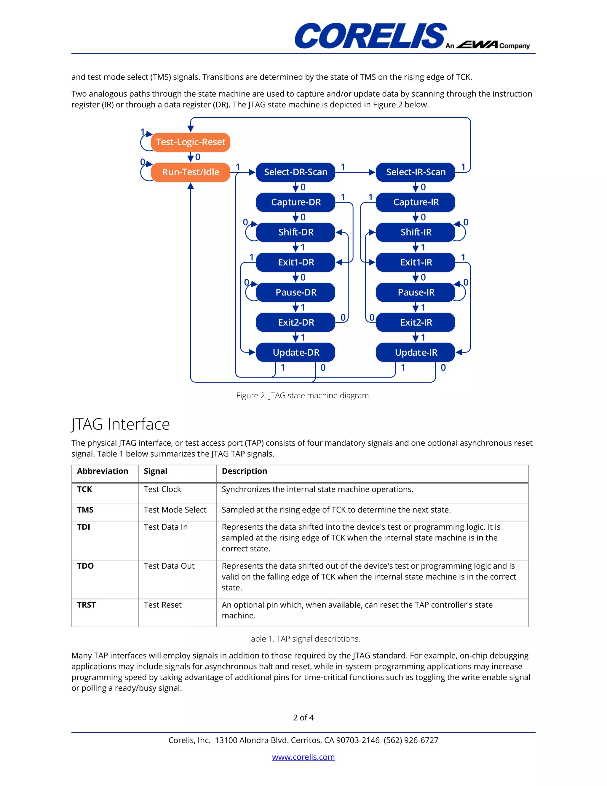
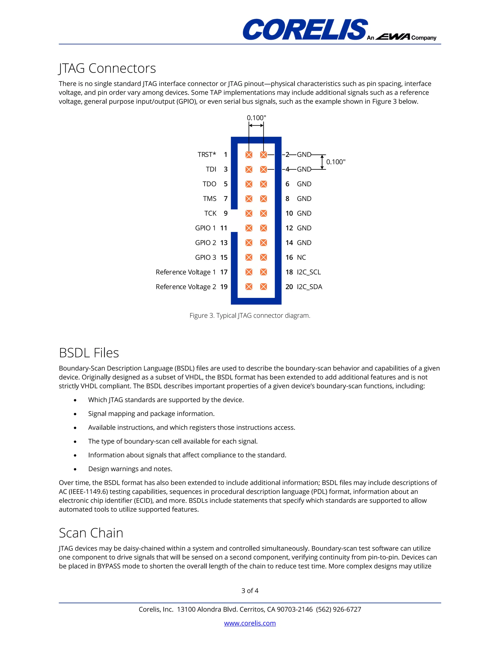
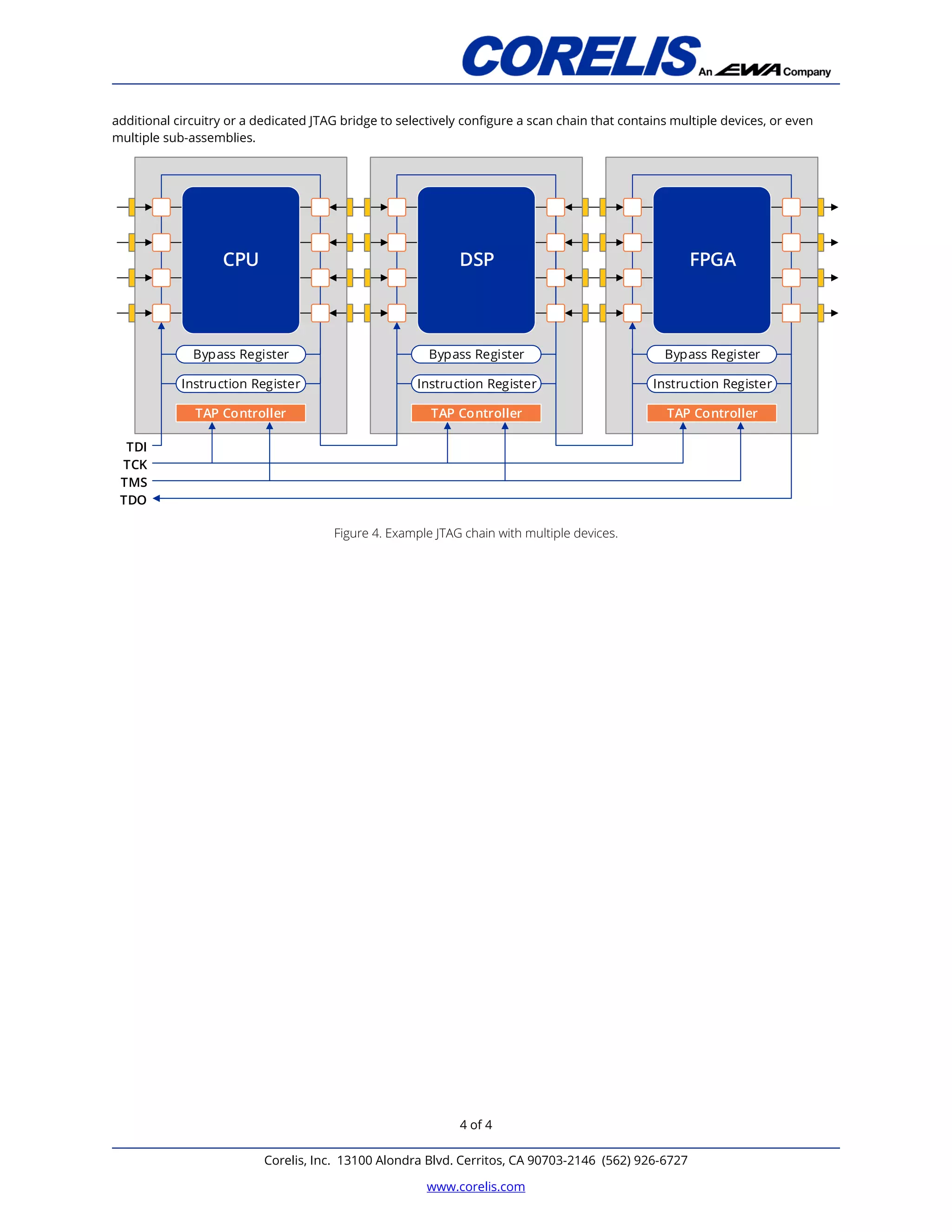
Corelis, Inc. 13100 Alondra Blvd. Cerritos, CA 90703-2146 (562) 926-6727
www.corelis.com
1 of 4
JTAG Technical Primer
Introduction
This primer provides a brief overview of JTAG devices--basic chip architecture, essential capabilities, and common system
configurations.
JTAG Chip Architecture
The IEEE-1149.1 JTAG standard defines how IC scan logic must
behave to achieve interoperability among components, systems,
and test tools. ICs consist of logic cells, or boundary-scan cells,
between the system logic and the signal pins or balls that
connect the IC to the PCB. Each cell provides specific test
capabilities—some cells can be used as input, others as output,
and some are bidirectional.
The boundary-scan cells within a device are connected together
to form a shift register, which is accessed through a serial test
data input (TDI) and test data output (TDO) interface. The Test
Access Port (TAP), consisting of 4 required signals and an
optional reset signal, is the primary interface to the test
controller which provides access to the logic.
JTAG Instructions
IEEE-1149.1 specifies mandatory instructions—to be fully JTAG
compliant, devices must utilize these instructions.
EXTEST
The EXTEST instruction is used to perform interconnect testing.
When the EXTEST instruction is used, the mandatory boundary-
scan register is connected between TDI and TDO and the device
is placed in an “external” test mode. In this mode, boundary-scan output cells will drive test data onto the device pins and
input cells will capture data from device pins—this is the main
instruction used for boundary-scan testing.
SAMPLE/PRELOAD
The SAMPLE/PRELOAD instruction is similar to EXTEST, but allows the boundary-scan device to remain in mission/functional
mode while still connecting the boundary-scan register to TDI and TDO. When the SAMPLE/PRELOAD instruction is used, the
boundary-scan register is accessible through data scans while the device remains functional. This is also useful for preloading
data into the boundary-scan register without interrupting the device’s functional behavior, prior to executing the EXTEST
instruction.
BYPASS
When the BYPASS instruction is used, TDI and TDO are connected to a single-bit register that bypasses the longer boundary-
scan register of the device—hence the name. BYPASS is very useful for reducing the overall length of a boundary-scan chain
by eliminating devices that do not need to be involved in the current action. Devices that are given the BYPASS instruction
remain in mission/functional mode while allowing serial data to flow through to the next device in the chain.
TAP Controller
The TAP controller as defined by the IEEE-1149.1 standard uses a 16-state finite state machine controlled by a test clock (TCK)
Design Specific Register
Core Logic
Device ID Register
Bypass Register
Instruction Decoder
Instruction Register
TAP
Controller
TDI TMS TCK TRST* TDO
Device
Inputs
Device
Outputs
Figure 1. Diagram of basic JTAG IC architecture.
Corelis, Inc. 13100 Alondra Blvd. Cerritos, CA 90703-2146 (562) 926-6727
www.corelis.com
2 of 4
and test mode select (TMS) signals. Transitions are determined by the state of TMS on the rising edge of TCK.
Two analogous paths through the state machine are used to capture and/or update data by scanning through the instruction
register (IR) or through a data register (DR). The JTAG state machine is depicted in Figure 2 below.
Figure 2. JTAG state machine diagram.
JTAG Interface
The physical JTAG interface, or test access port (TAP) consists of four mandatory signals and one optional asynchronous reset
signal. Table 1 below summarizes the JTAG TAP signals.
Abbreviation Signal Description
TCK Test Clock Synchronizes the internal state machine operations.
TMS Test Mode Select Sampled at the rising edge of TCK to determine the next state.
TDI Test Data In Represents the data shifted into the device's test or programming logic. It is
sampled at the rising edge of TCK when the internal state machine is in the
correct state.
TDO Test Data Out Represents the data shifted out of the device's test or programming logic and is
valid on the falling edge of TCK when the internal state machine is in the correct
state.
TRST Test Reset An optional pin which, when available, can reset the TAP controller's state
machine.
Table 1. TAP signal descriptions.
Many TAP interfaces will employ signals in addition to those required by the JTAG standard. For example, on-chip debugging
applications may include signals for asynchronous halt and reset, while in-system-programming applications may increase
programming speed by taking advantage of additional pins for time-critical functions such as toggling the write enable signal
or polling a ready/busy signal.
Test-Logic-Reset
Run-Test/Idle Select-DR-Scan
Capture-DR
Shift-DR
Exit1-DR
Pause-DR
Exit2-DR
Update-DR
0
0
1
1
0
1
1
Select-IR-Scan
Capture-IR
Shift-IR
Exit1-IR
Pause-IR
Exit2-IR
0
0
1
1
0
1
1
Update-IR
0
1 1
1 1
0
1 0 1 0
1
0
1
0
0 0
0
0
1
1
Corelis, Inc. 13100 Alondra Blvd. Cerritos, CA 90703-2146 (562) 926-6727
www.corelis.com
3 of 4
JTAG Connectors
There is no single standard JTAG interface connector or JTAG pinout—physical characteristics such as pin spacing, interface
voltage, and pin order vary among devices. Some TAP implementations may include additional signals such as a reference
voltage, general purpose input/output (GPIO), or even serial bus signals, such as the example shown in Figure 3 below.
20
18
16
14
12
10
8
6
4
2
19
17
15
13
11
9
7
5
3
1
Reference Voltage 1
GPIO 3
GPIO 2
GPIO 1
TDO
TCK
TMS
TRST*
TDI
Reference Voltage 2
GND
NC
I2C_SCL
I2C_SDA
GND
GND
GND
GND
GND
GND
0.100"
0.100"
Figure 3. Typical JTAG connector diagram.
BSDL Files
Boundary-Scan Description Language (BSDL) files are used to describe the boundary-scan behavior and capabilities of a given
device. Originally designed as a subset of VHDL, the BSDL format has been extended to add additional features and is not
strictly VHDL compliant. The BSDL describes important properties of a given device’s boundary-scan functions, including:
 Which JTAG standards are supported by the device.
 Signal mapping and package information.
 Available instructions, and which registers those instructions access.
 The type of boundary-scan cell available for each signal.
 Information about signals that affect compliance to the standard.
 Design warnings and notes.
Over time, the BSDL format has also been extended to include additional information; BSDL files may include descriptions of
AC (IEEE-1149.6) testing capabilities, sequences in procedural description language (PDL) format, information about an
electronic chip identifier (ECID), and more. BSDLs include statements that specify which standards are supported to allow
automated tools to utilize supported features.
Scan Chain
JTAG devices may be daisy-chained within a system and controlled simultaneously. Boundary-scan test software can utilize
one component to drive signals that will be sensed on a second component, verifying continuity from pin-to-pin. Devices can
be placed in BYPASS mode to shorten the overall length of the chain to reduce test time. More complex designs may utilize
Corelis, Inc. 13100 Alondra Blvd. Cerritos, CA 90703-2146 (562) 926-6727
www.corelis.com
4 of 4
additional circuitry or a dedicated JTAG bridge to selectively configure a scan chain that contains multiple devices, or even
multiple sub-assemblies.
Figure 4. Example JTAG chain with multiple devices.
CPU
Bypass Register
Instruction Register
TAP Controller
Bypass Register
Instruction Register
TAP Controller
DSP
Bypass Register
Instruction Register
TAP Controller
FPGA
TDI
TMS
TCK
TDO

JTAG-Technical-Primer.pdf

  • 1.
    Corelis, Inc. 13100Alondra Blvd. Cerritos, CA 90703-2146 (562) 926-6727 www.corelis.com 1 of 4 JTAG Technical Primer Introduction This primer provides a brief overview of JTAG devices--basic chip architecture, essential capabilities, and common system configurations. JTAG Chip Architecture The IEEE-1149.1 JTAG standard defines how IC scan logic must behave to achieve interoperability among components, systems, and test tools. ICs consist of logic cells, or boundary-scan cells, between the system logic and the signal pins or balls that connect the IC to the PCB. Each cell provides specific test capabilities—some cells can be used as input, others as output, and some are bidirectional. The boundary-scan cells within a device are connected together to form a shift register, which is accessed through a serial test data input (TDI) and test data output (TDO) interface. The Test Access Port (TAP), consisting of 4 required signals and an optional reset signal, is the primary interface to the test controller which provides access to the logic. JTAG Instructions IEEE-1149.1 specifies mandatory instructions—to be fully JTAG compliant, devices must utilize these instructions. EXTEST The EXTEST instruction is used to perform interconnect testing. When the EXTEST instruction is used, the mandatory boundary- scan register is connected between TDI and TDO and the device is placed in an “external” test mode. In this mode, boundary-scan output cells will drive test data onto the device pins and input cells will capture data from device pins—this is the main instruction used for boundary-scan testing. SAMPLE/PRELOAD The SAMPLE/PRELOAD instruction is similar to EXTEST, but allows the boundary-scan device to remain in mission/functional mode while still connecting the boundary-scan register to TDI and TDO. When the SAMPLE/PRELOAD instruction is used, the boundary-scan register is accessible through data scans while the device remains functional. This is also useful for preloading data into the boundary-scan register without interrupting the device’s functional behavior, prior to executing the EXTEST instruction. BYPASS When the BYPASS instruction is used, TDI and TDO are connected to a single-bit register that bypasses the longer boundary- scan register of the device—hence the name. BYPASS is very useful for reducing the overall length of a boundary-scan chain by eliminating devices that do not need to be involved in the current action. Devices that are given the BYPASS instruction remain in mission/functional mode while allowing serial data to flow through to the next device in the chain. TAP Controller The TAP controller as defined by the IEEE-1149.1 standard uses a 16-state finite state machine controlled by a test clock (TCK) Design Specific Register Core Logic Device ID Register Bypass Register Instruction Decoder Instruction Register TAP Controller TDI TMS TCK TRST* TDO Device Inputs Device Outputs Figure 1. Diagram of basic JTAG IC architecture.
  • 2.
    Corelis, Inc. 13100Alondra Blvd. Cerritos, CA 90703-2146 (562) 926-6727 www.corelis.com 2 of 4 and test mode select (TMS) signals. Transitions are determined by the state of TMS on the rising edge of TCK. Two analogous paths through the state machine are used to capture and/or update data by scanning through the instruction register (IR) or through a data register (DR). The JTAG state machine is depicted in Figure 2 below. Figure 2. JTAG state machine diagram. JTAG Interface The physical JTAG interface, or test access port (TAP) consists of four mandatory signals and one optional asynchronous reset signal. Table 1 below summarizes the JTAG TAP signals. Abbreviation Signal Description TCK Test Clock Synchronizes the internal state machine operations. TMS Test Mode Select Sampled at the rising edge of TCK to determine the next state. TDI Test Data In Represents the data shifted into the device's test or programming logic. It is sampled at the rising edge of TCK when the internal state machine is in the correct state. TDO Test Data Out Represents the data shifted out of the device's test or programming logic and is valid on the falling edge of TCK when the internal state machine is in the correct state. TRST Test Reset An optional pin which, when available, can reset the TAP controller's state machine. Table 1. TAP signal descriptions. Many TAP interfaces will employ signals in addition to those required by the JTAG standard. For example, on-chip debugging applications may include signals for asynchronous halt and reset, while in-system-programming applications may increase programming speed by taking advantage of additional pins for time-critical functions such as toggling the write enable signal or polling a ready/busy signal. Test-Logic-Reset Run-Test/Idle Select-DR-Scan Capture-DR Shift-DR Exit1-DR Pause-DR Exit2-DR Update-DR 0 0 1 1 0 1 1 Select-IR-Scan Capture-IR Shift-IR Exit1-IR Pause-IR Exit2-IR 0 0 1 1 0 1 1 Update-IR 0 1 1 1 1 0 1 0 1 0 1 0 1 0 0 0 0 0 1 1
  • 3.
    Corelis, Inc. 13100Alondra Blvd. Cerritos, CA 90703-2146 (562) 926-6727 www.corelis.com 3 of 4 JTAG Connectors There is no single standard JTAG interface connector or JTAG pinout—physical characteristics such as pin spacing, interface voltage, and pin order vary among devices. Some TAP implementations may include additional signals such as a reference voltage, general purpose input/output (GPIO), or even serial bus signals, such as the example shown in Figure 3 below. 20 18 16 14 12 10 8 6 4 2 19 17 15 13 11 9 7 5 3 1 Reference Voltage 1 GPIO 3 GPIO 2 GPIO 1 TDO TCK TMS TRST* TDI Reference Voltage 2 GND NC I2C_SCL I2C_SDA GND GND GND GND GND GND 0.100" 0.100" Figure 3. Typical JTAG connector diagram. BSDL Files Boundary-Scan Description Language (BSDL) files are used to describe the boundary-scan behavior and capabilities of a given device. Originally designed as a subset of VHDL, the BSDL format has been extended to add additional features and is not strictly VHDL compliant. The BSDL describes important properties of a given device’s boundary-scan functions, including:  Which JTAG standards are supported by the device.  Signal mapping and package information.  Available instructions, and which registers those instructions access.  The type of boundary-scan cell available for each signal.  Information about signals that affect compliance to the standard.  Design warnings and notes. Over time, the BSDL format has also been extended to include additional information; BSDL files may include descriptions of AC (IEEE-1149.6) testing capabilities, sequences in procedural description language (PDL) format, information about an electronic chip identifier (ECID), and more. BSDLs include statements that specify which standards are supported to allow automated tools to utilize supported features. Scan Chain JTAG devices may be daisy-chained within a system and controlled simultaneously. Boundary-scan test software can utilize one component to drive signals that will be sensed on a second component, verifying continuity from pin-to-pin. Devices can be placed in BYPASS mode to shorten the overall length of the chain to reduce test time. More complex designs may utilize
  • 4.
    Corelis, Inc. 13100Alondra Blvd. Cerritos, CA 90703-2146 (562) 926-6727 www.corelis.com 4 of 4 additional circuitry or a dedicated JTAG bridge to selectively configure a scan chain that contains multiple devices, or even multiple sub-assemblies. Figure 4. Example JTAG chain with multiple devices. CPU Bypass Register Instruction Register TAP Controller Bypass Register Instruction Register TAP Controller DSP Bypass Register Instruction Register TAP Controller FPGA TDI TMS TCK TDO