Downloaded 153 times


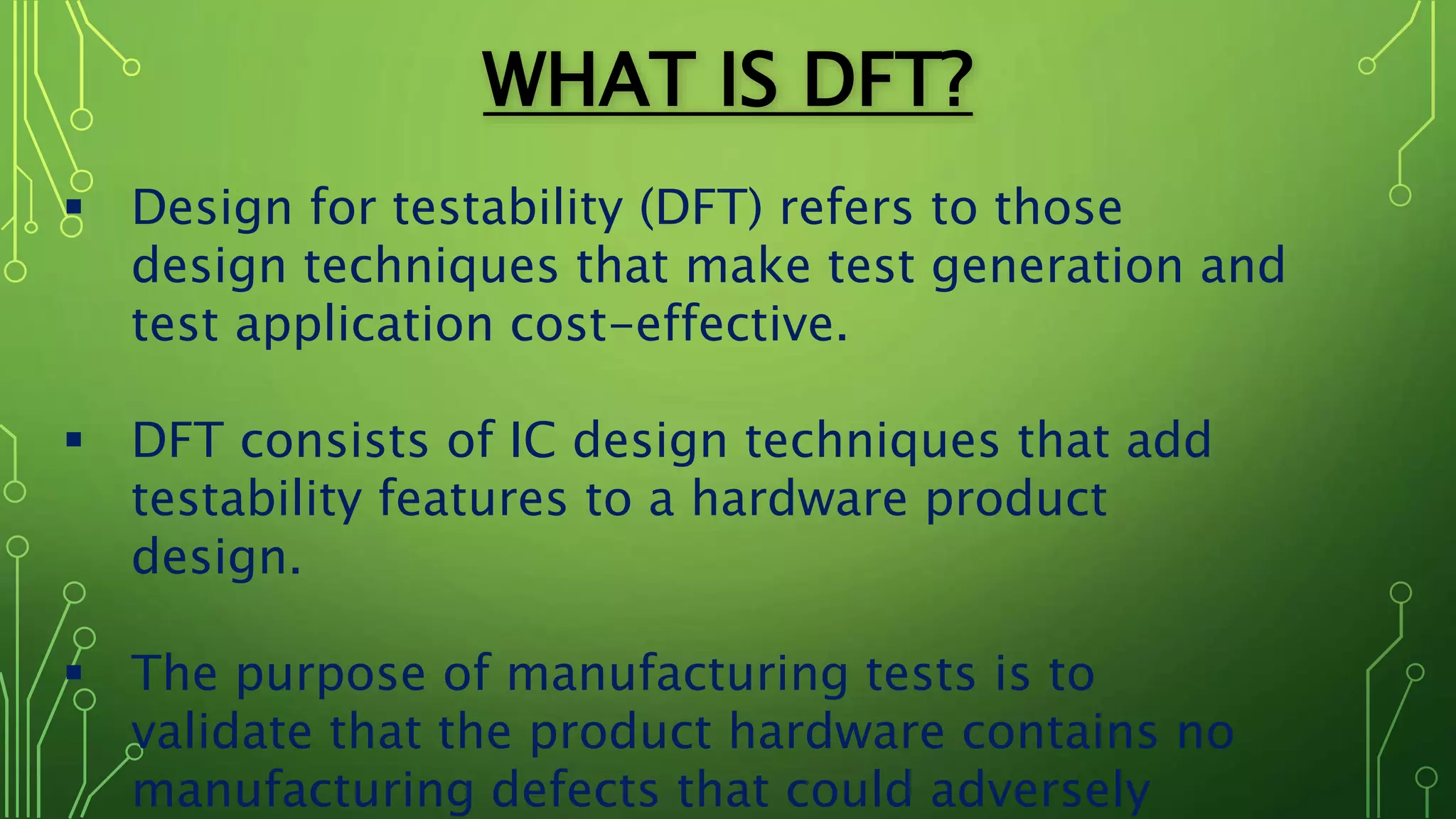


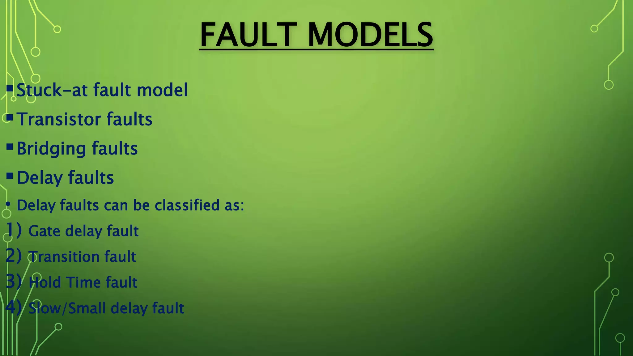
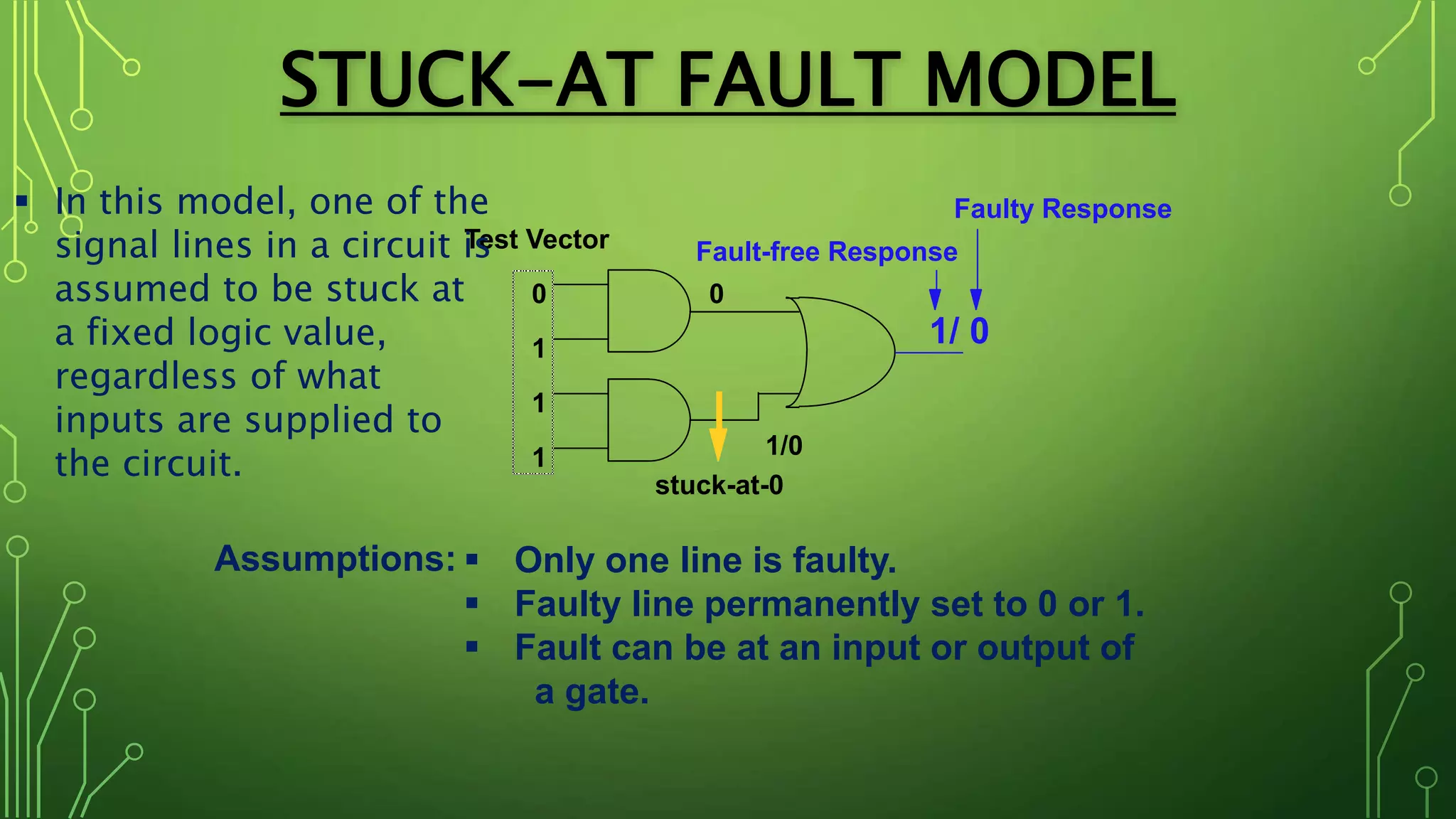
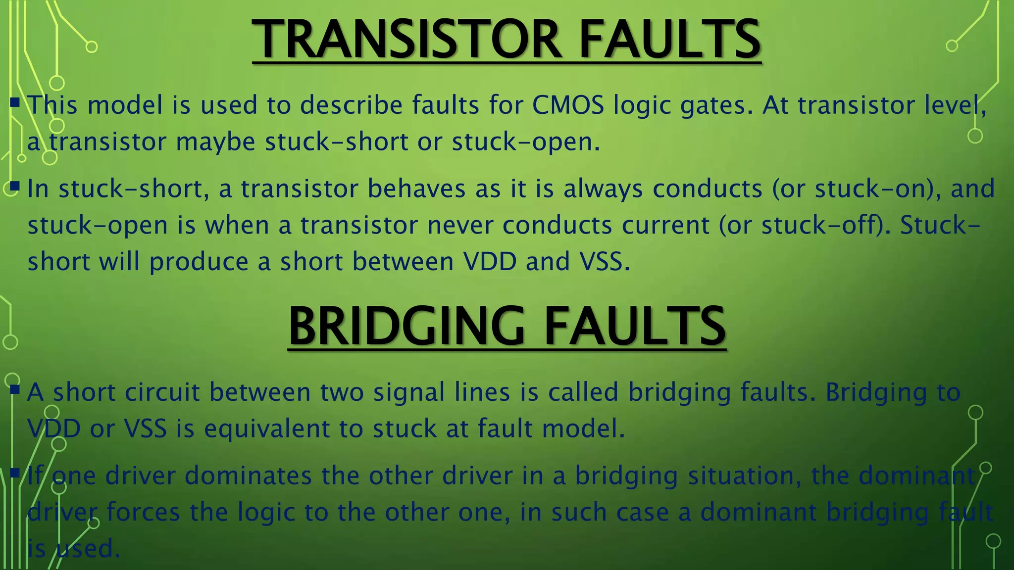
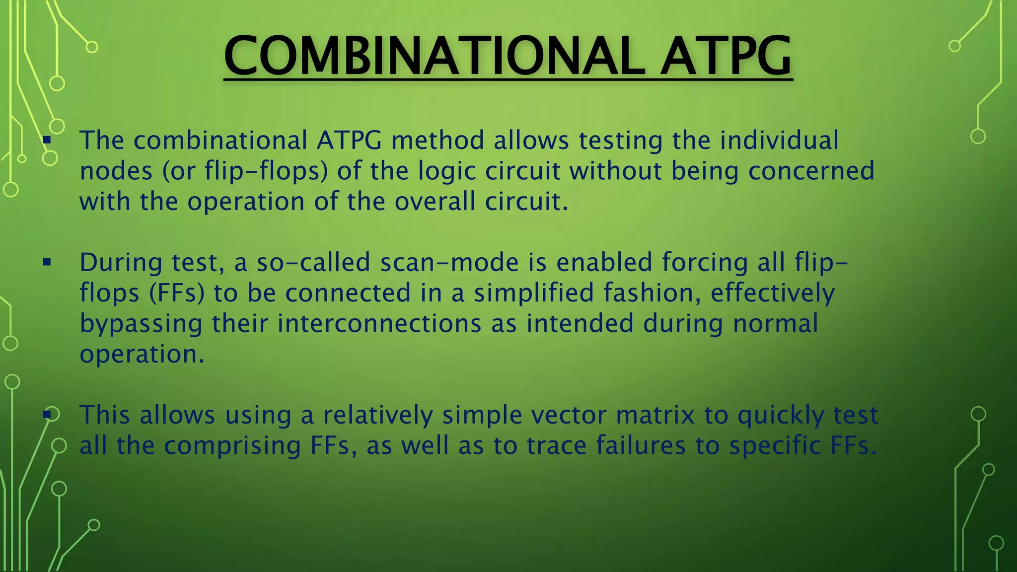

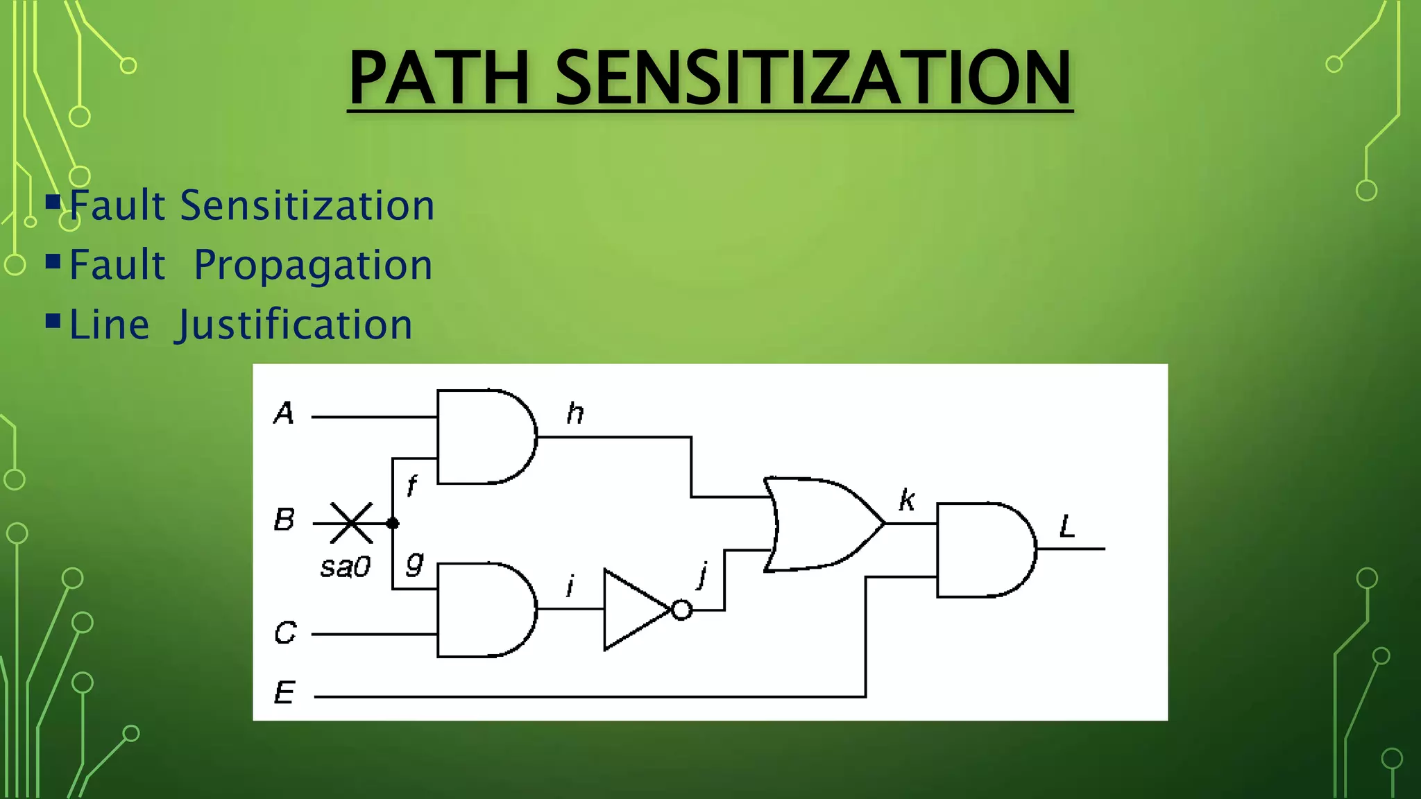
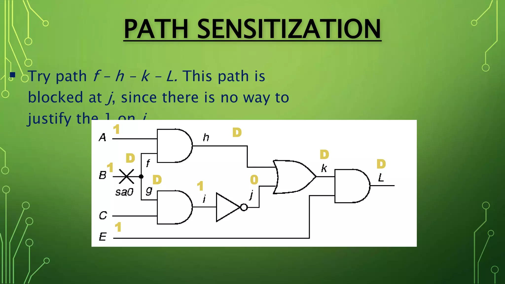
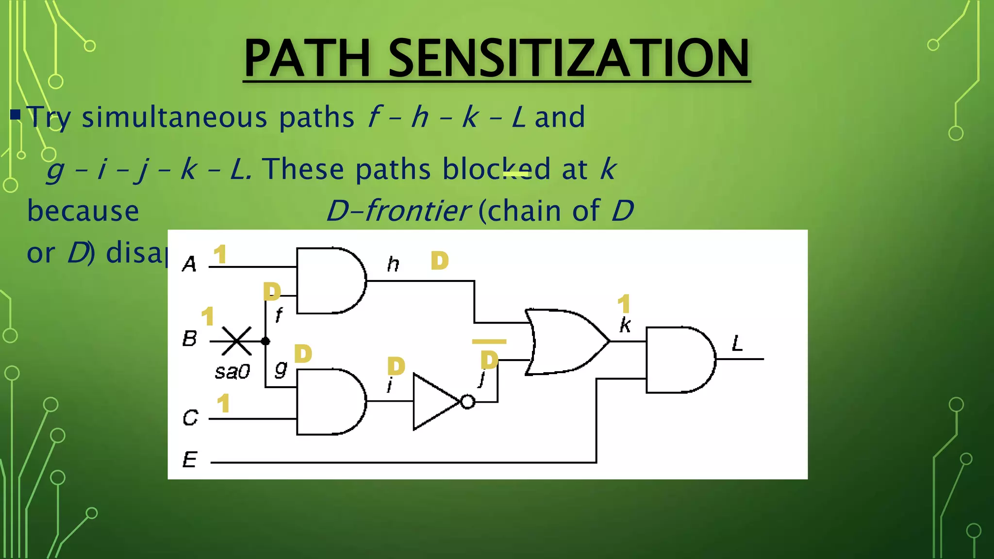


The document discusses Design for Testability (DFT) and automatic test pattern generation, emphasizing the importance of making integrated circuit designs more testable and cost-effective. It covers various DFT methods, including ad-hoc, structured methods like scan design, and Built-In Self-Test (BIST), alongside the economic implications of testing at various production stages. Additionally, it details fault models such as stuck-at faults, bridging faults, and the principles of automatic test pattern generation to enhance testing efficiency and effectiveness.


![Design for Test [DFT]-1 (1).pdf DESIGN DFT](https://cdn.slidesharecdn.com/ss_thumbnails/designfortestdft-11-231227151941-28a508a3-thumbnail.jpg?width=640&height=640&fit=bounds)