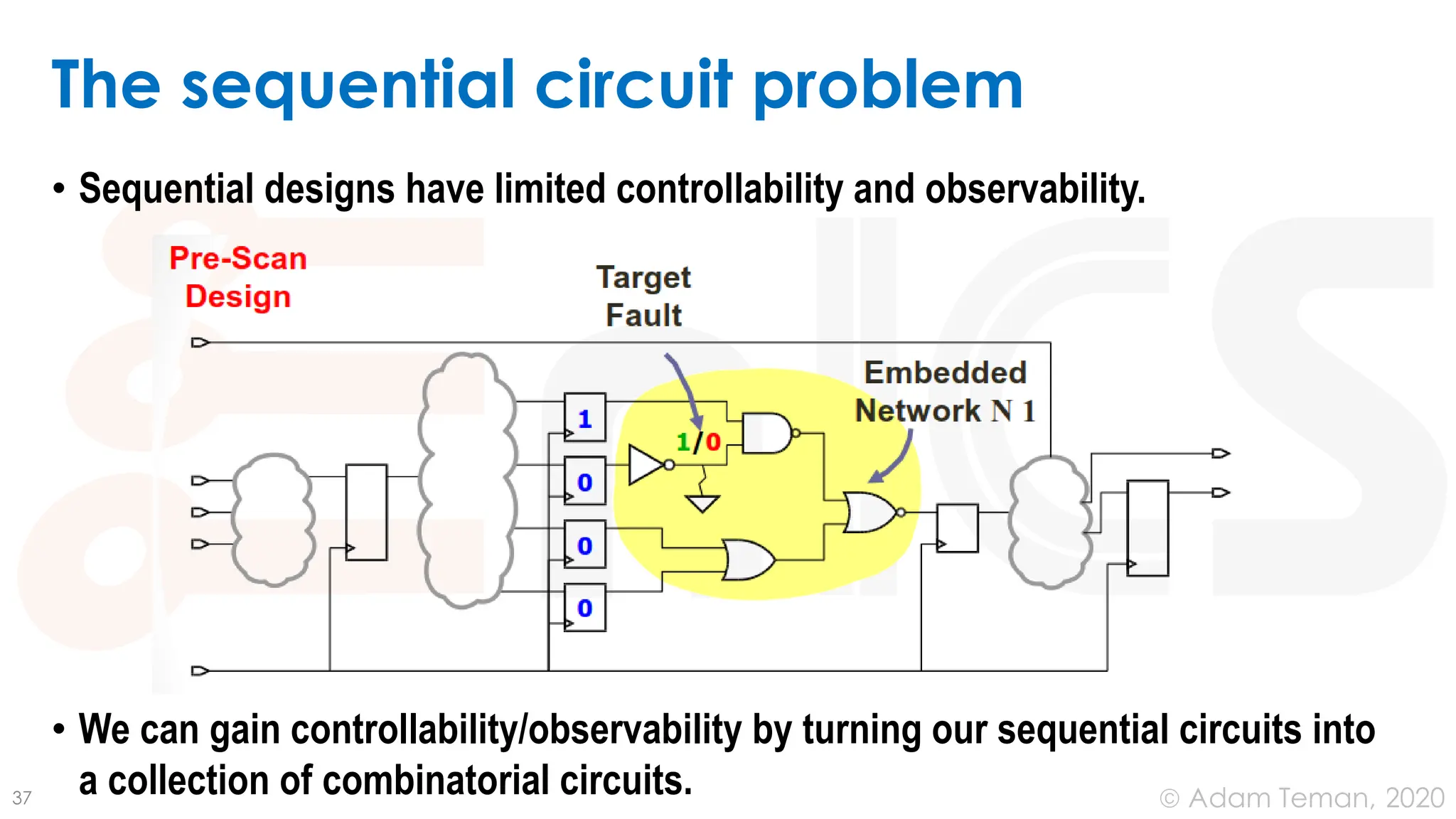
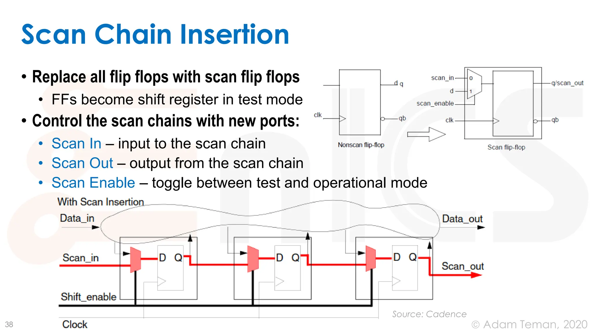
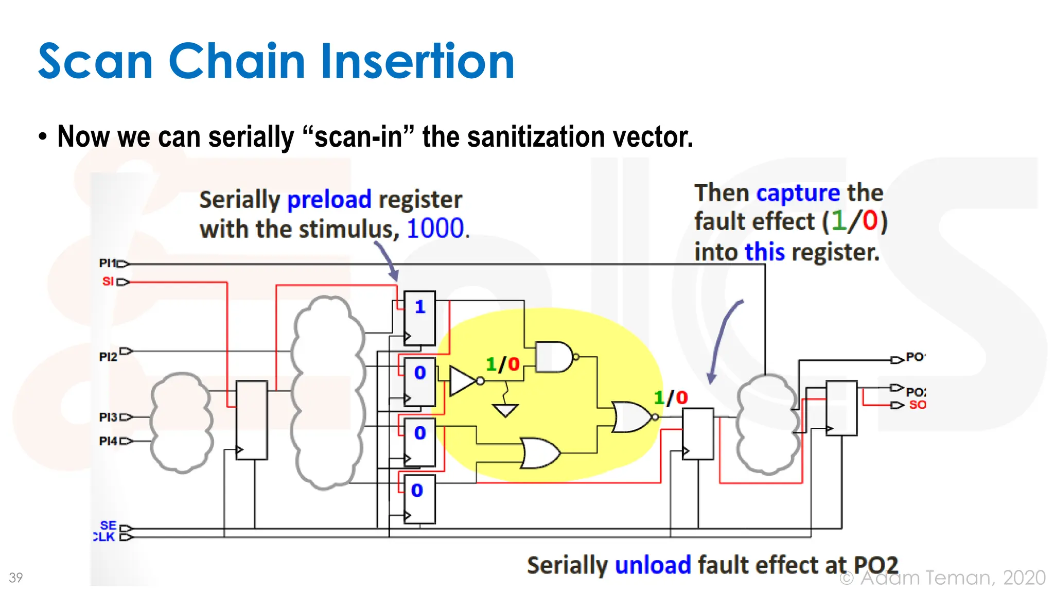
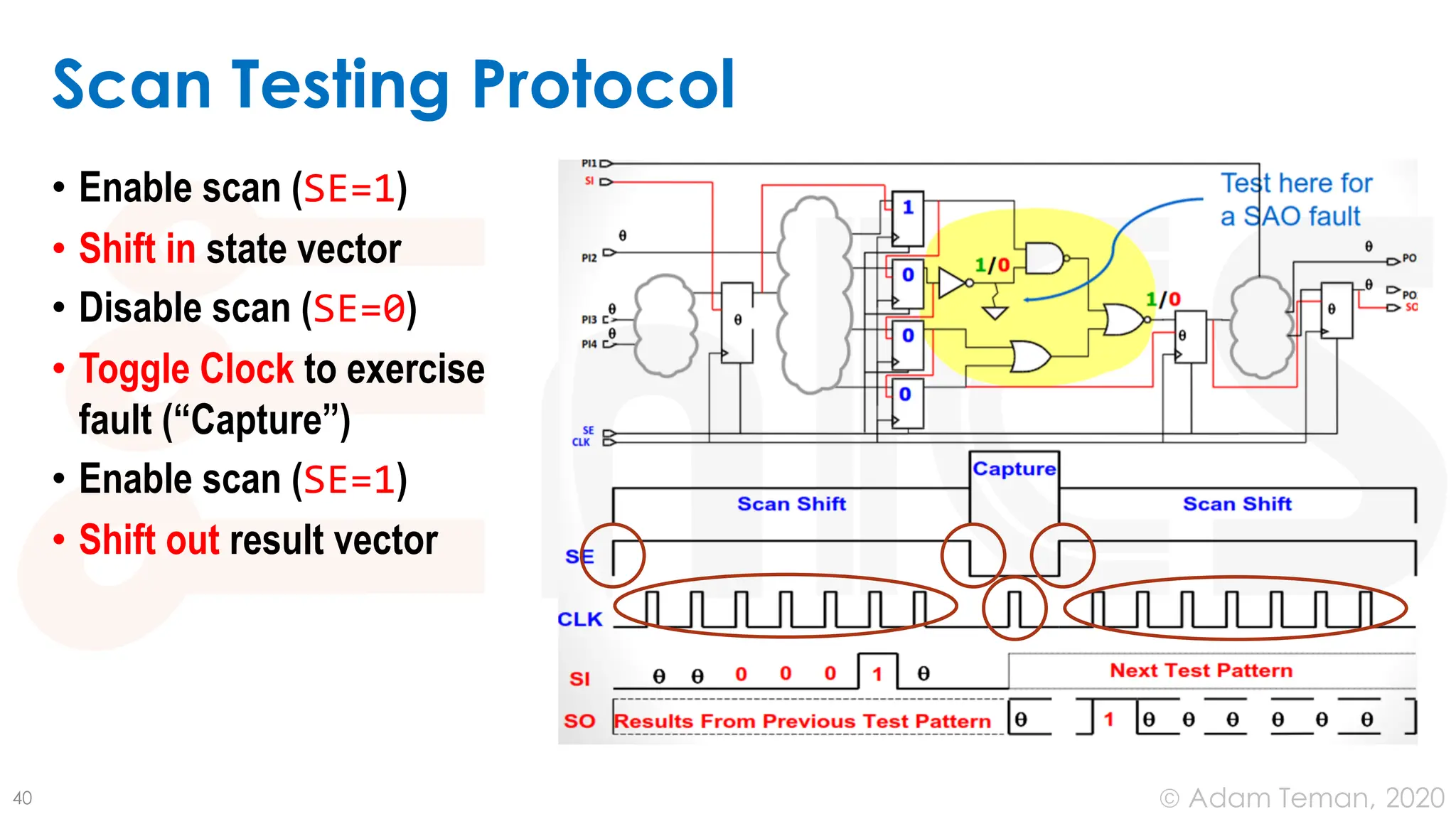
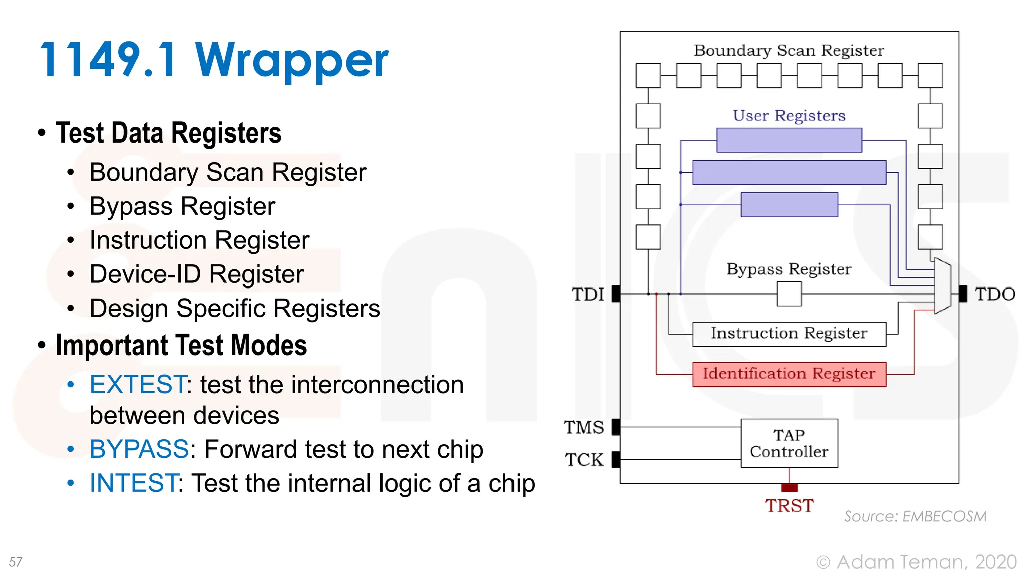
This document discusses design for test (DFT) and integrated circuit testing. It covers:
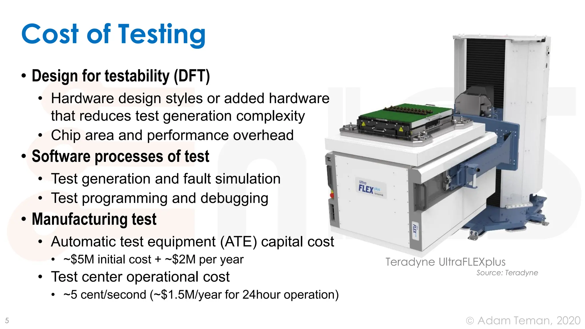
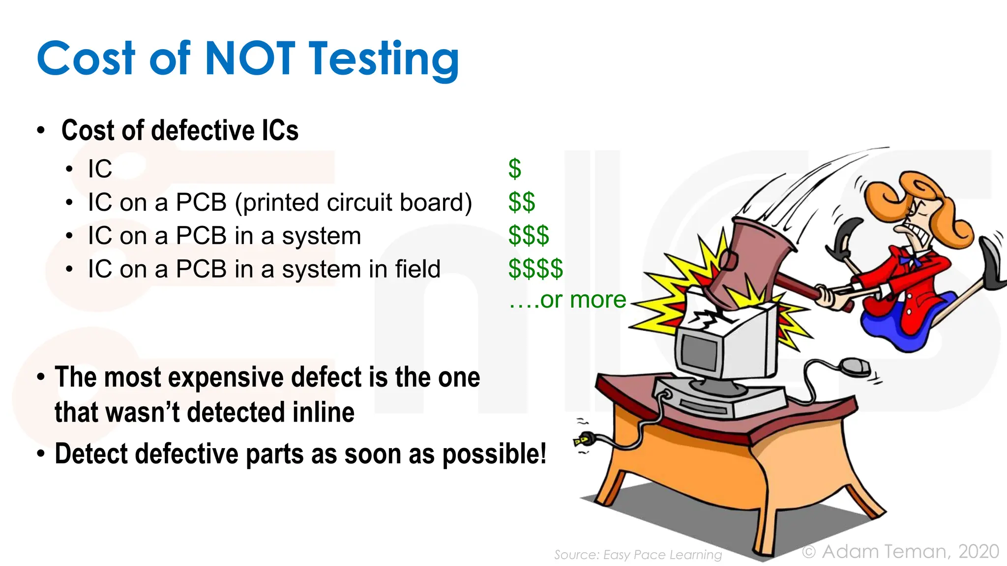
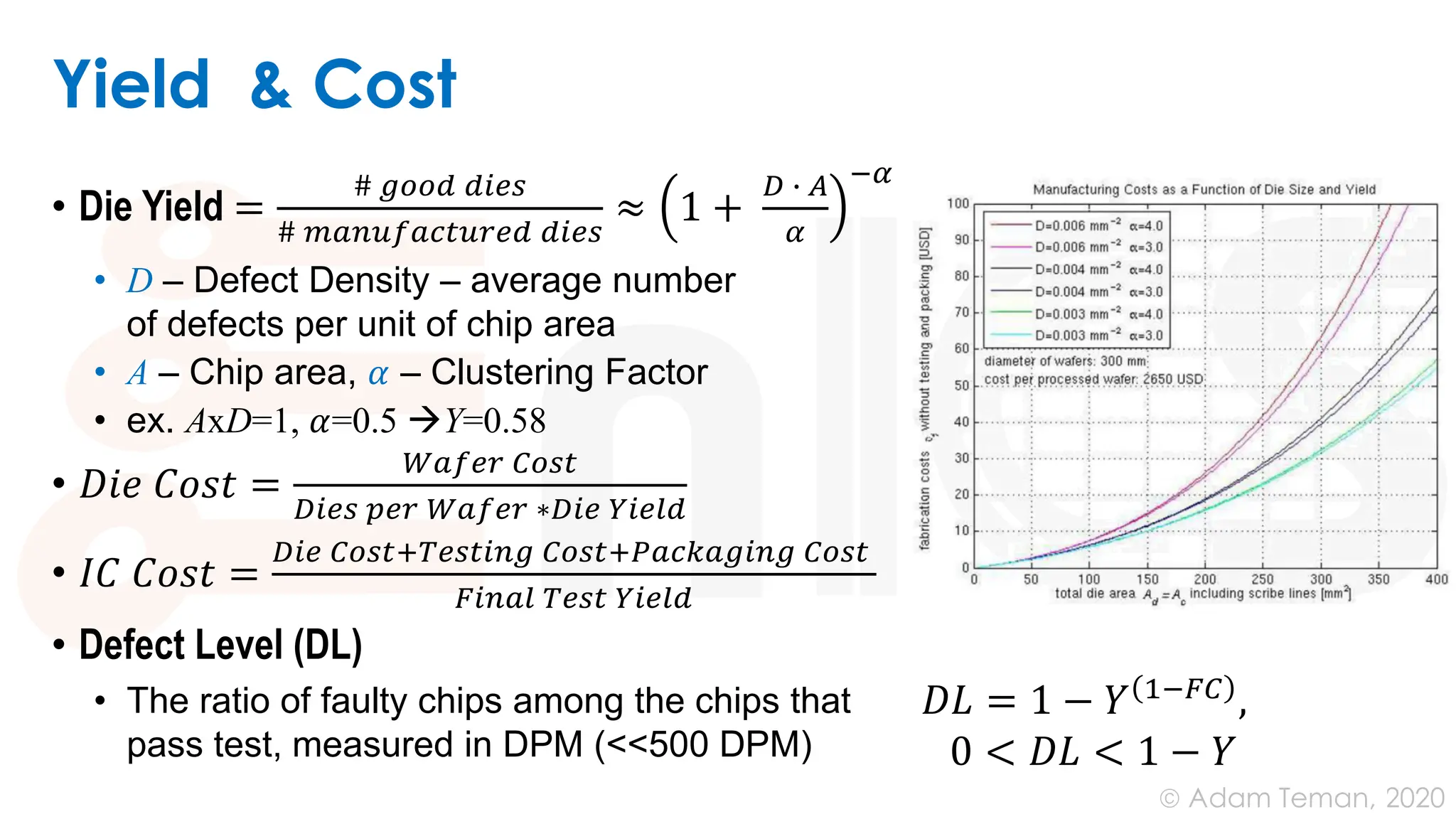
- The costs of testing including automatic test equipment, test generation software, and the high costs of defects found after manufacturing.
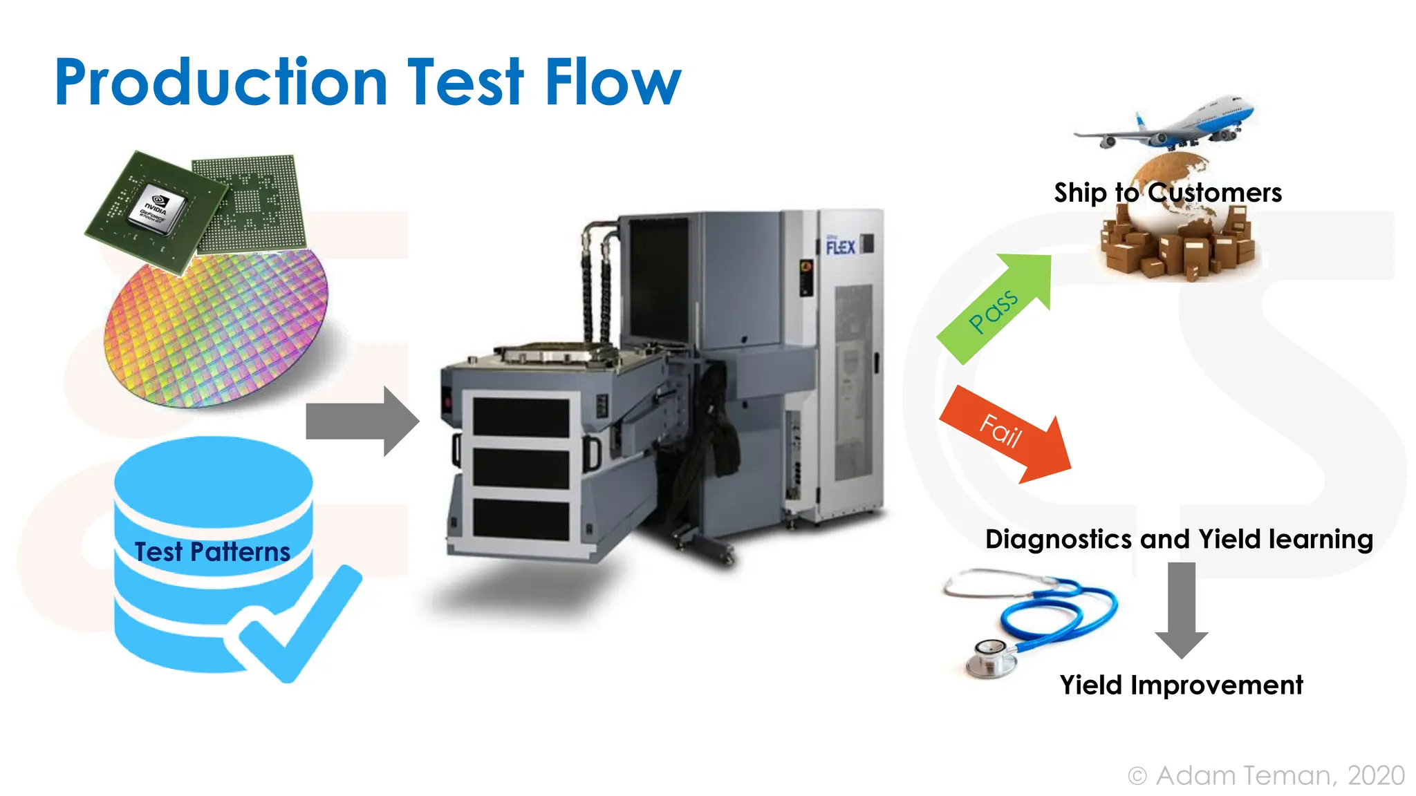
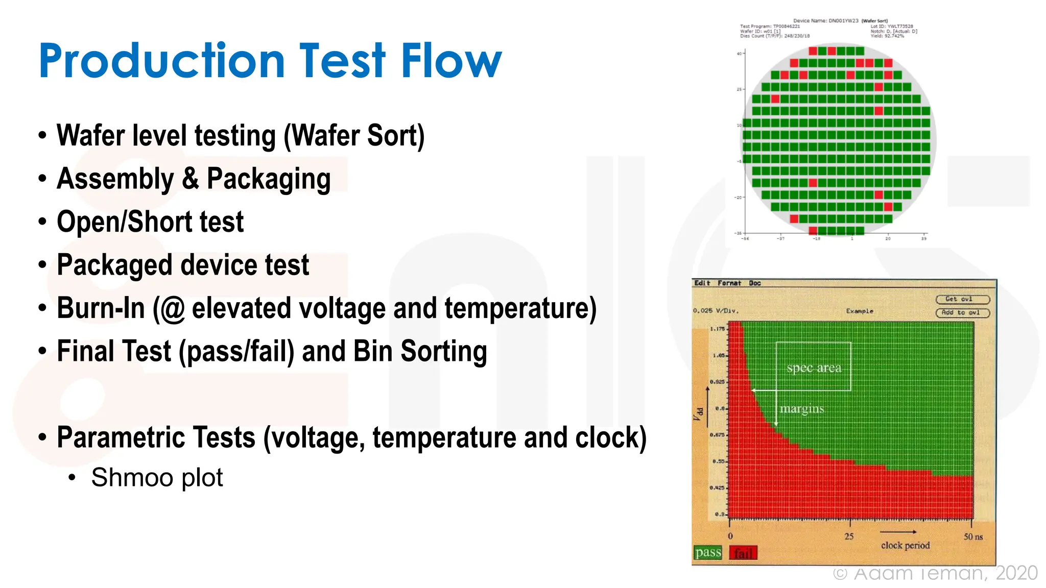
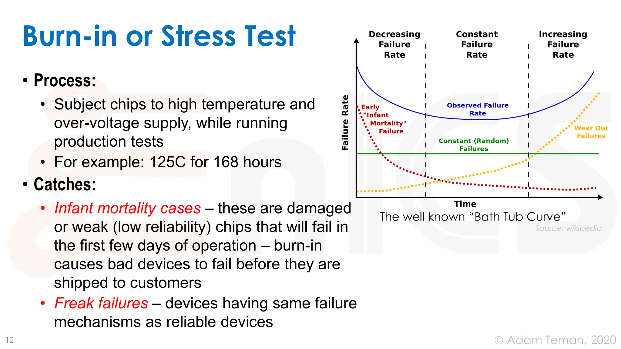
- The production test flow including wafer sorting, assembly and packaging tests, burn-in testing, and final testing before product is shipped.
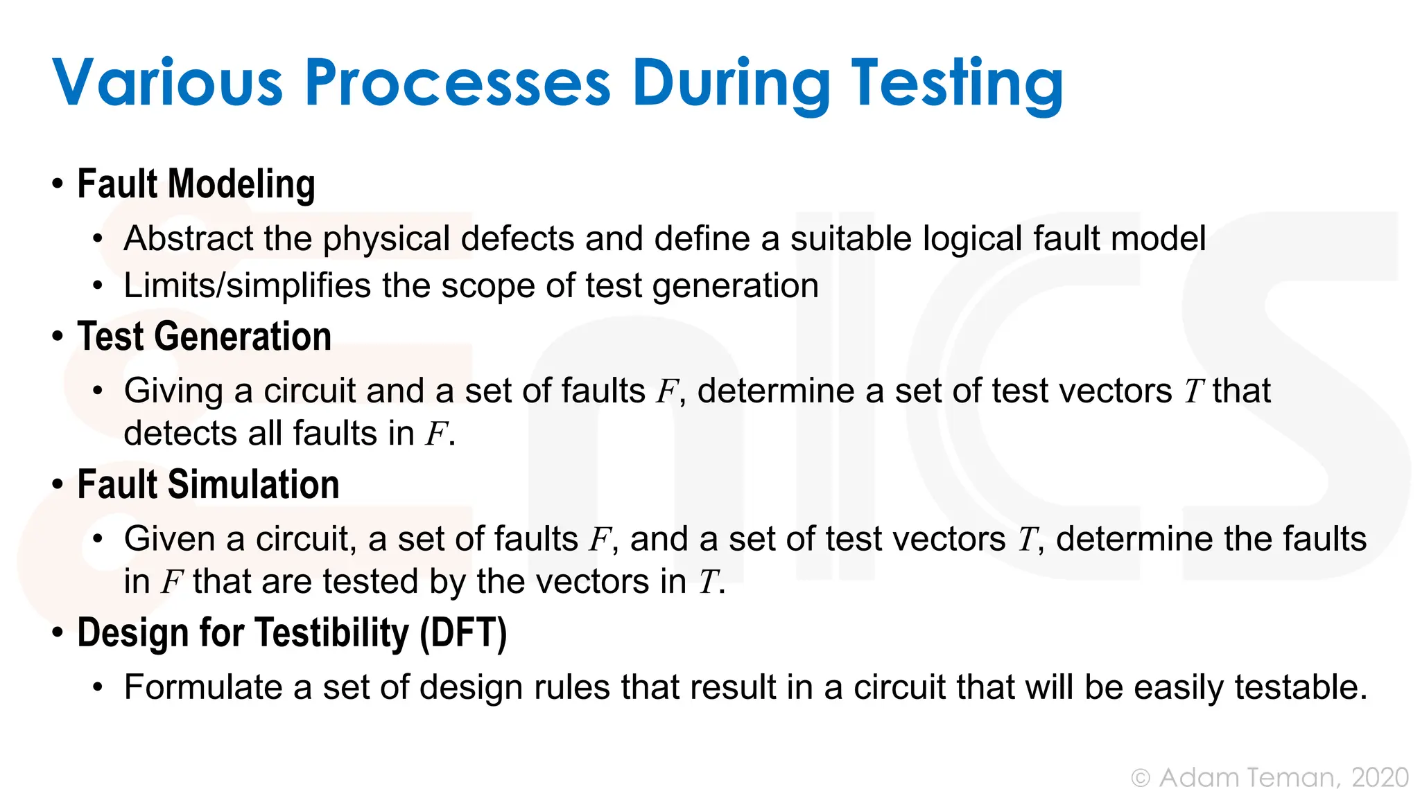
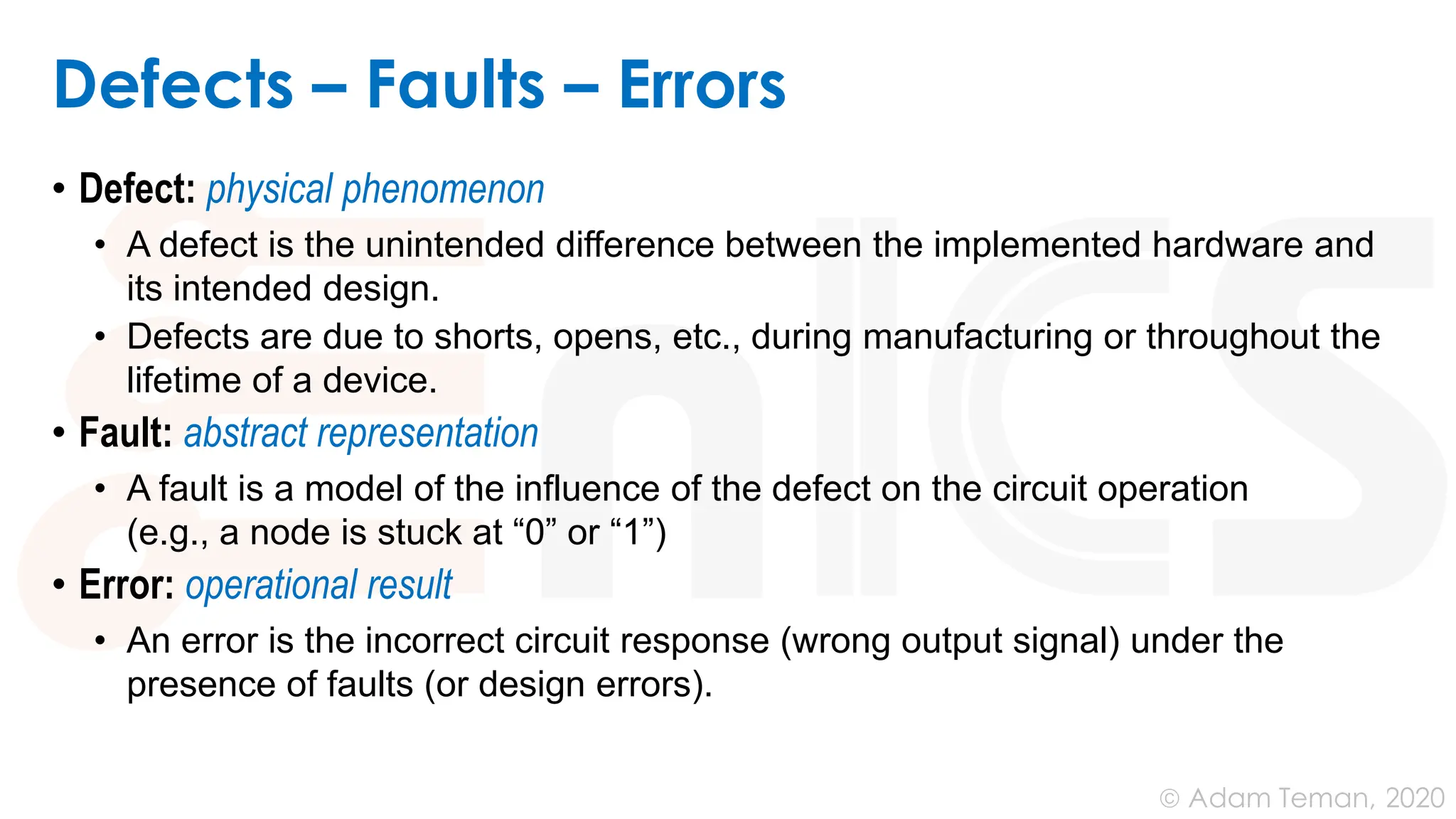
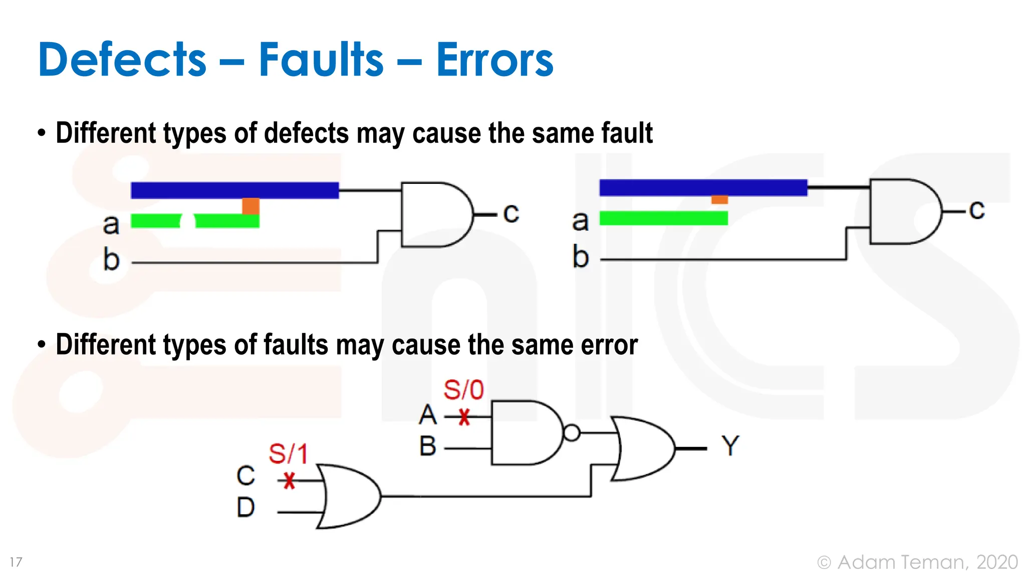
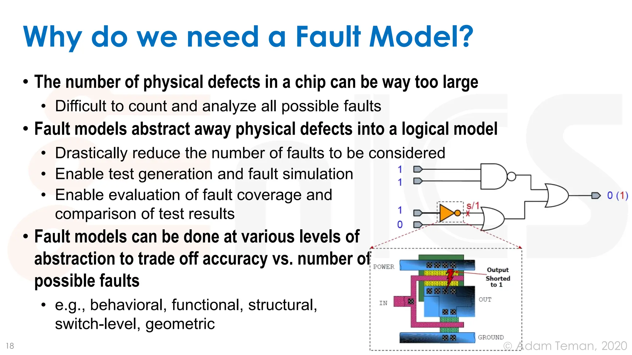
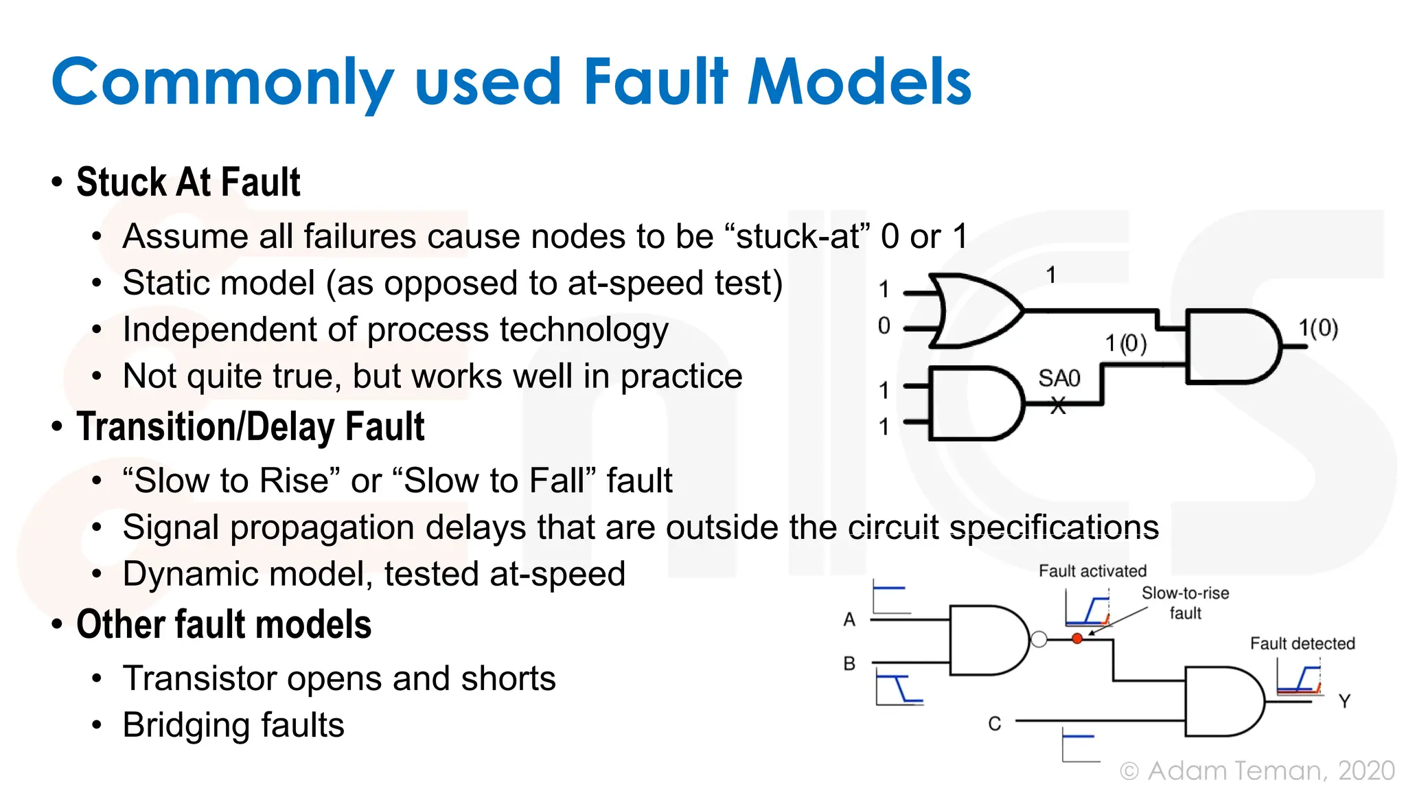
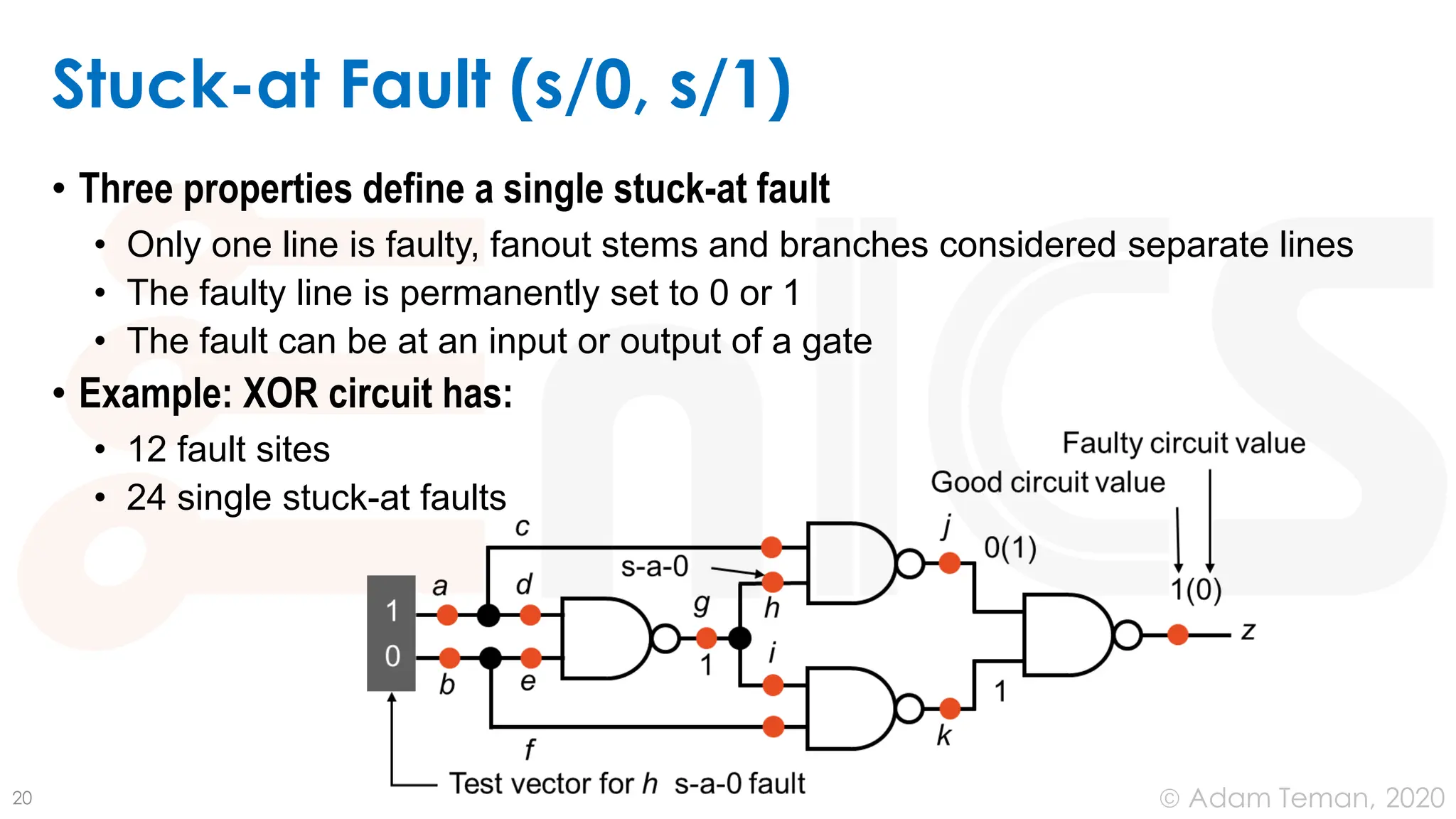
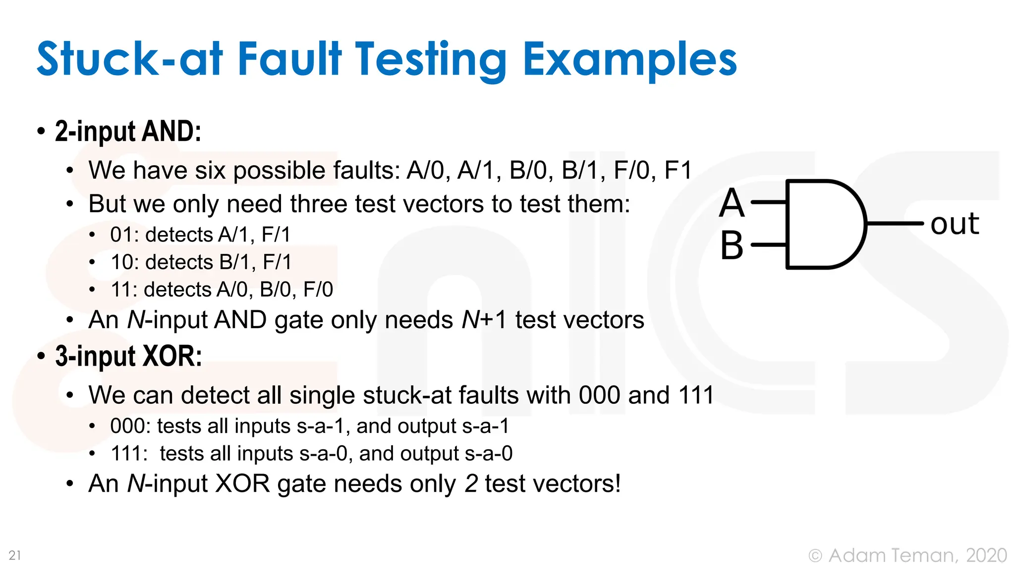
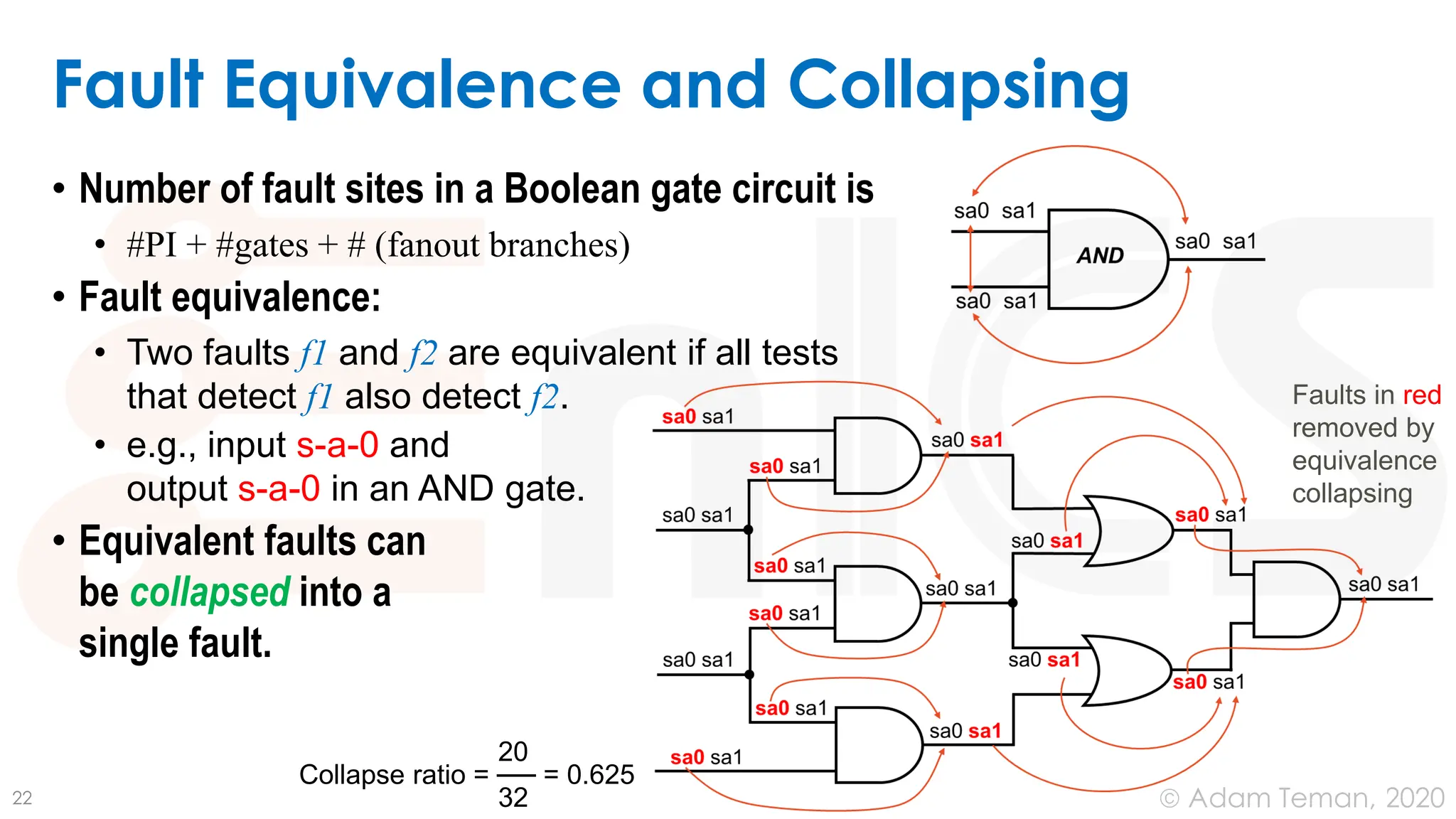
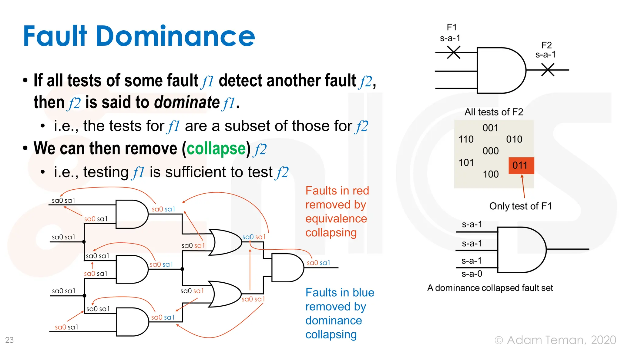
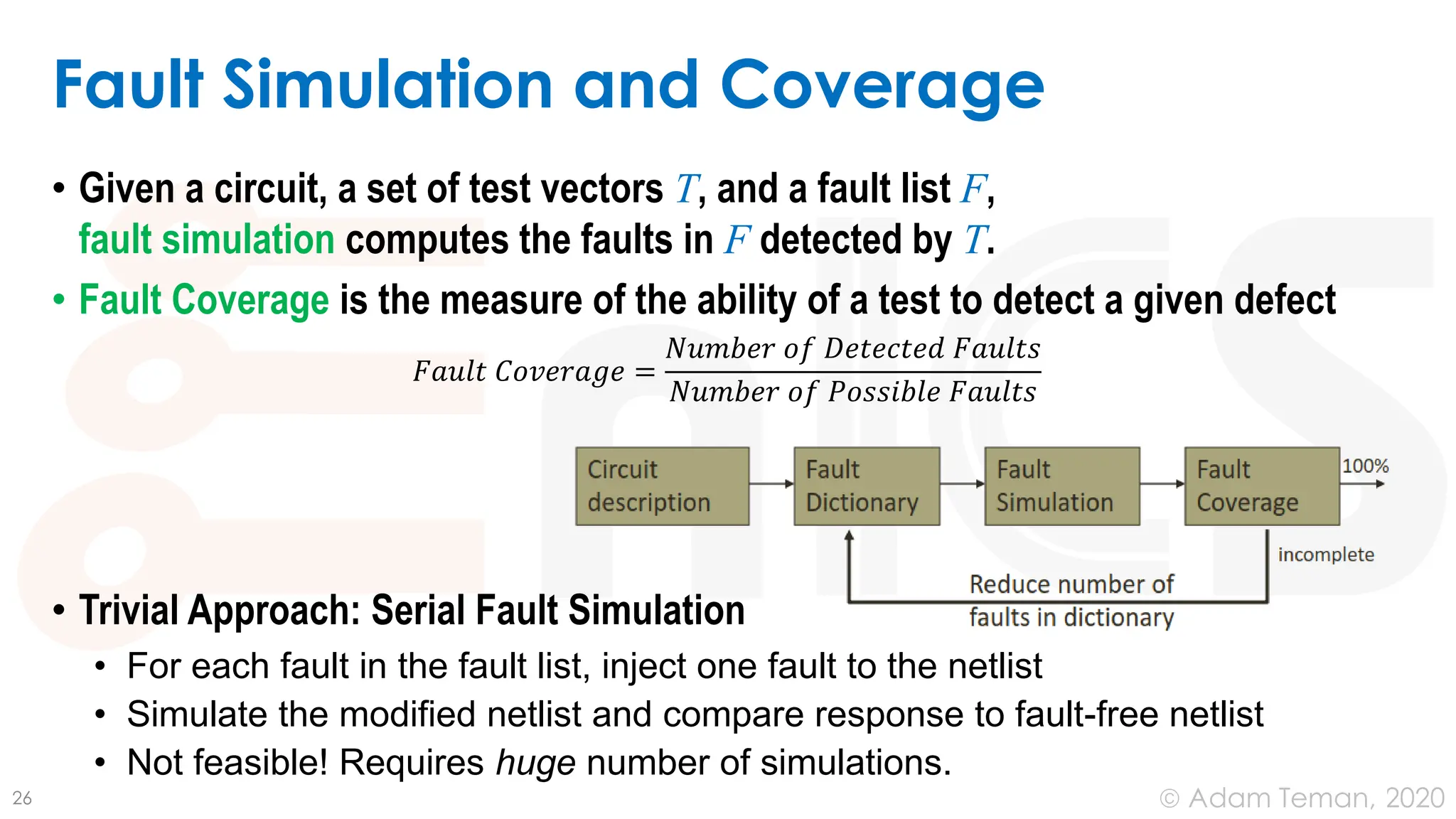
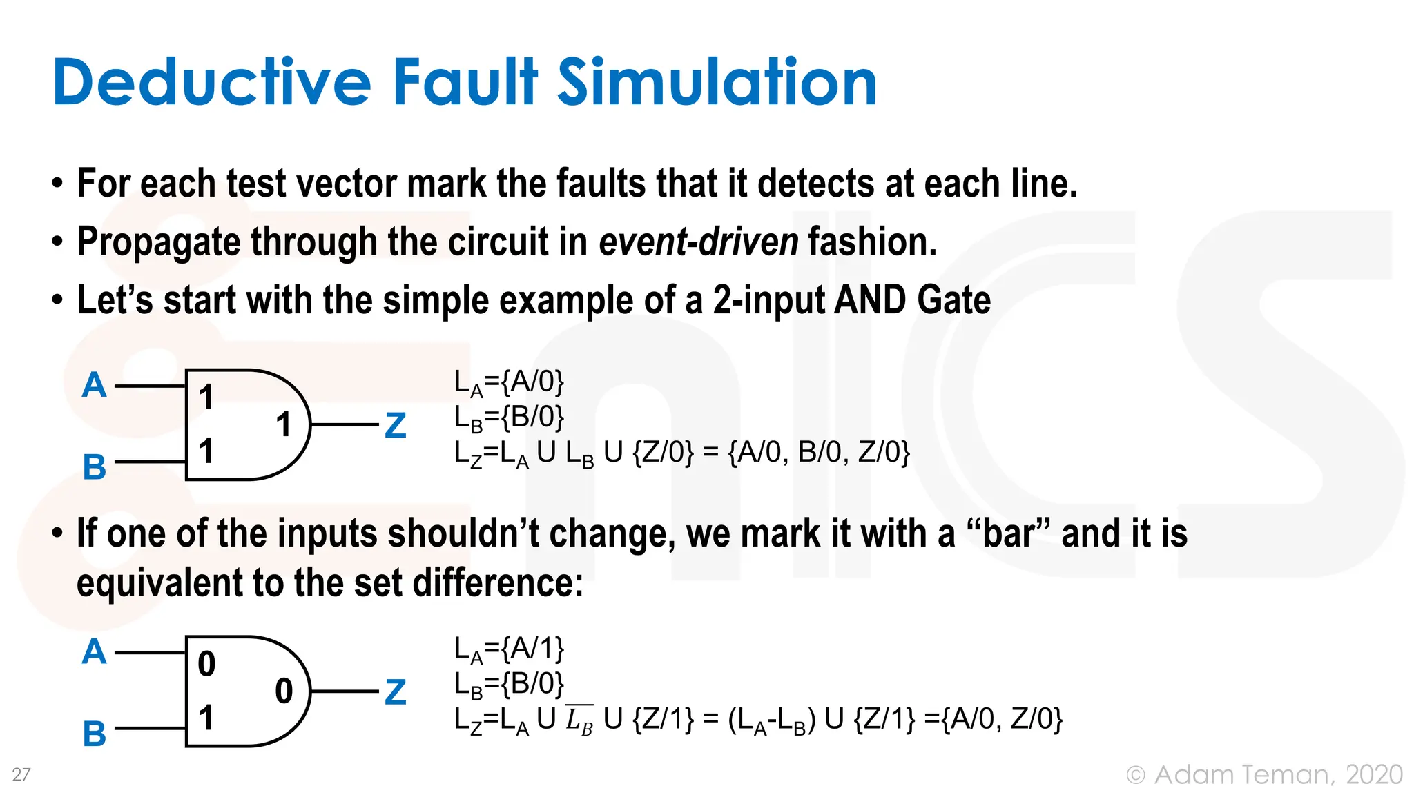
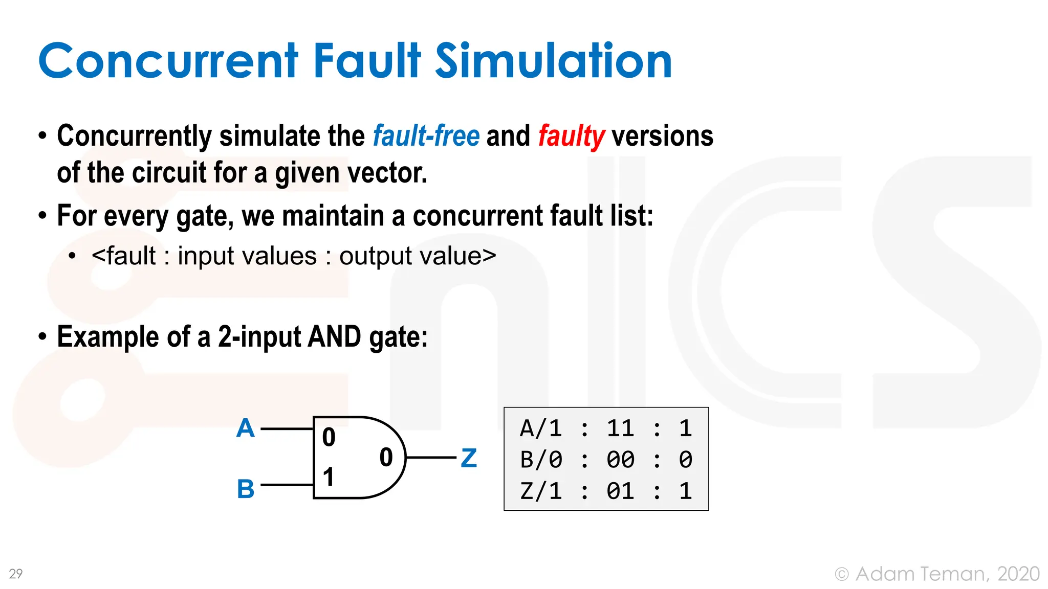
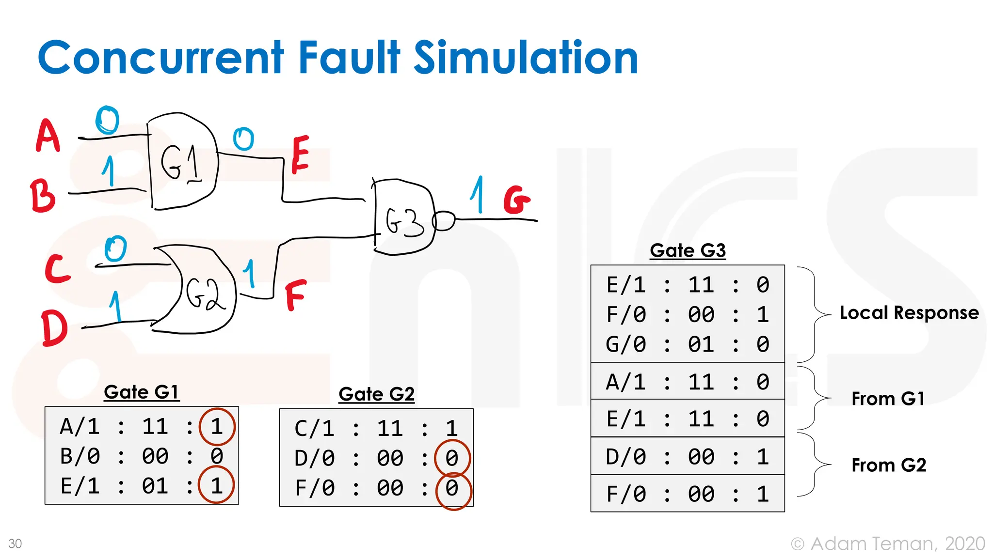
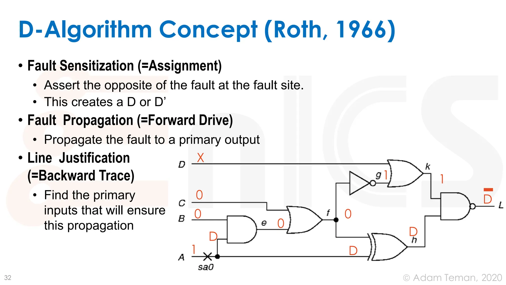
- Common fault models like stuck-at faults that are used to model defects and simplify testing. Deductive and concurrent fault simulation techniques are also discussed.


![Design for Test [DFT]-1 (1).pdf DESIGN DFT](https://cdn.slidesharecdn.com/ss_thumbnails/designfortestdft-11-231227151941-28a508a3-thumbnail.jpg?width=640&height=640&fit=bounds)