Downloaded 1,123 times
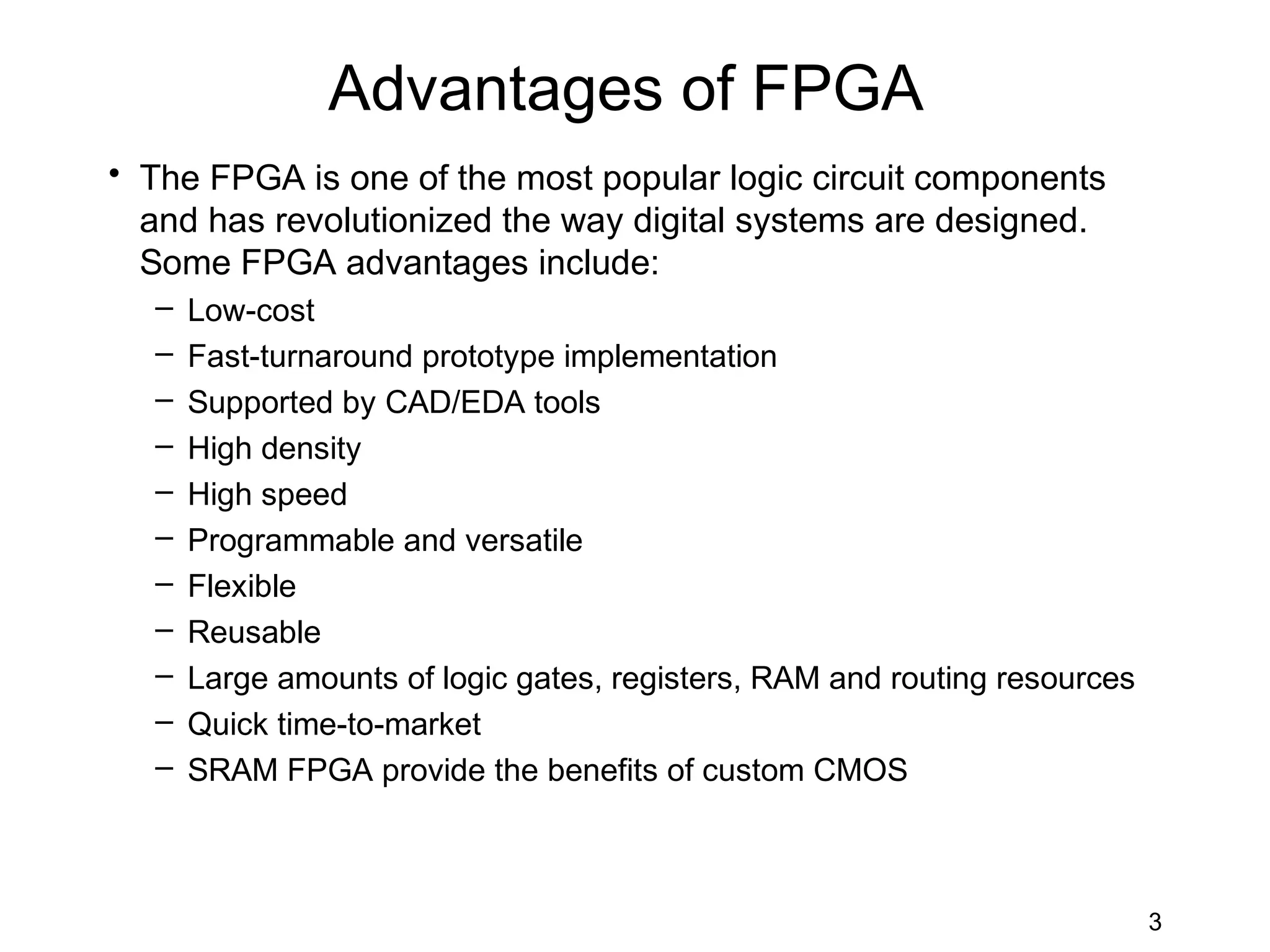
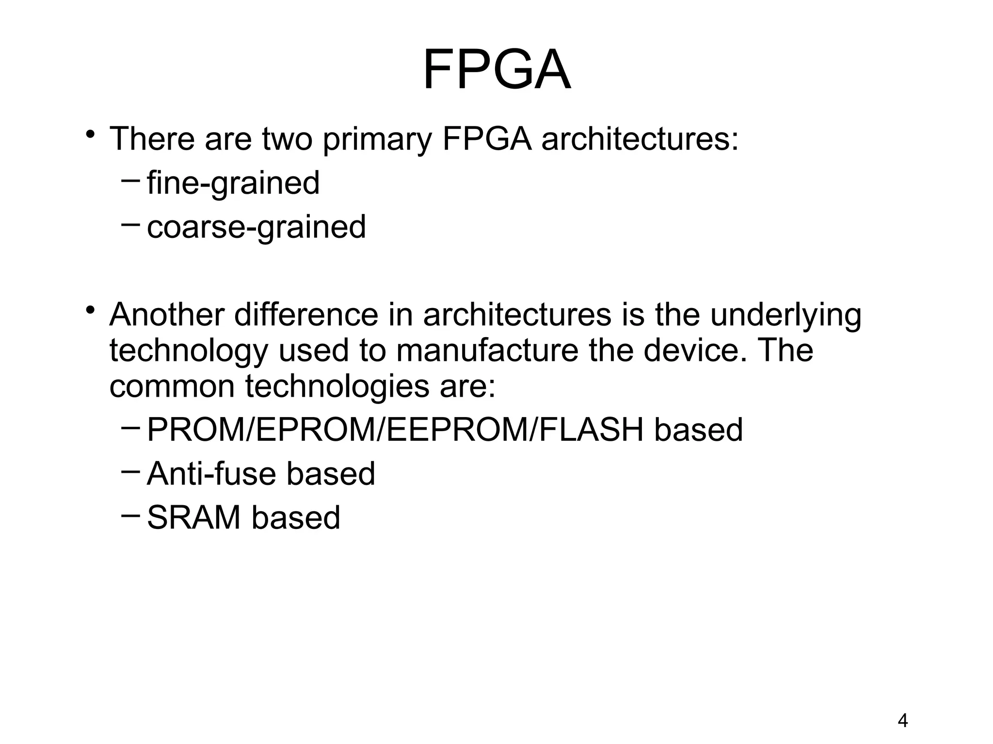
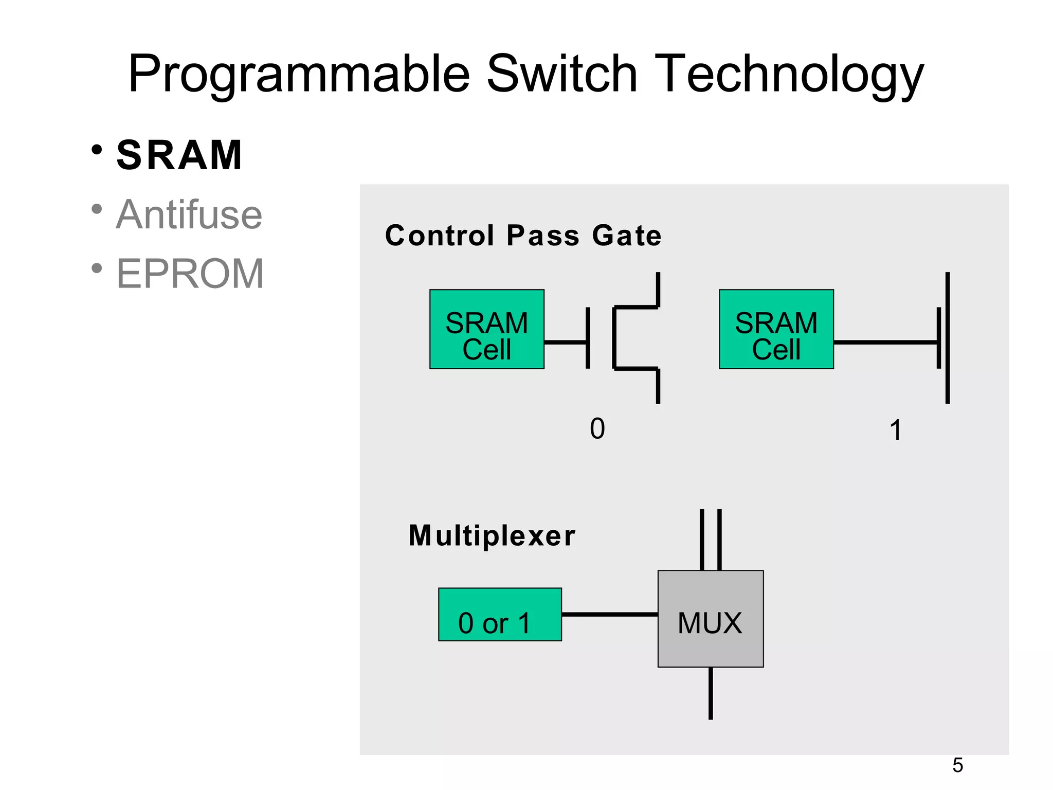
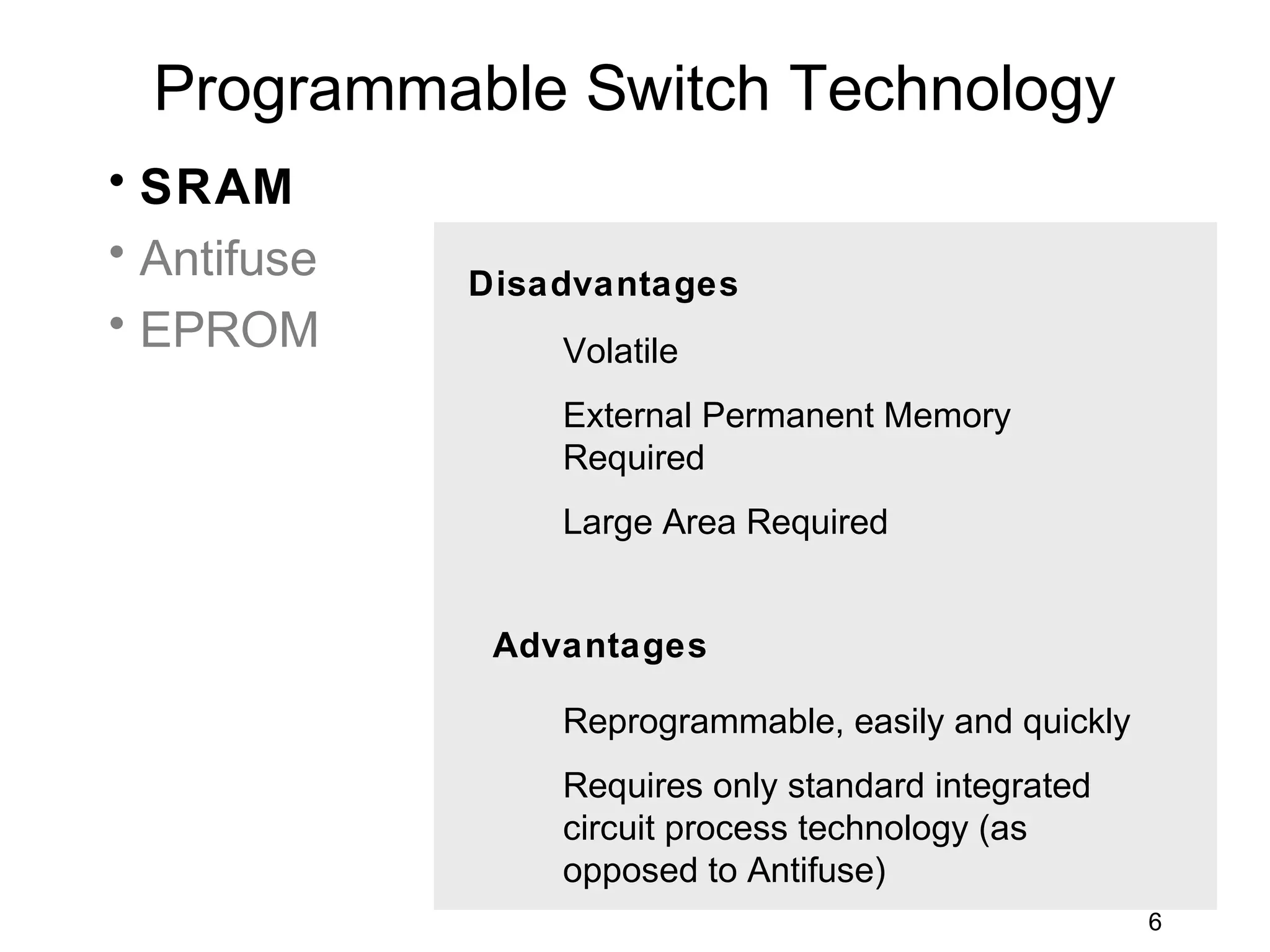
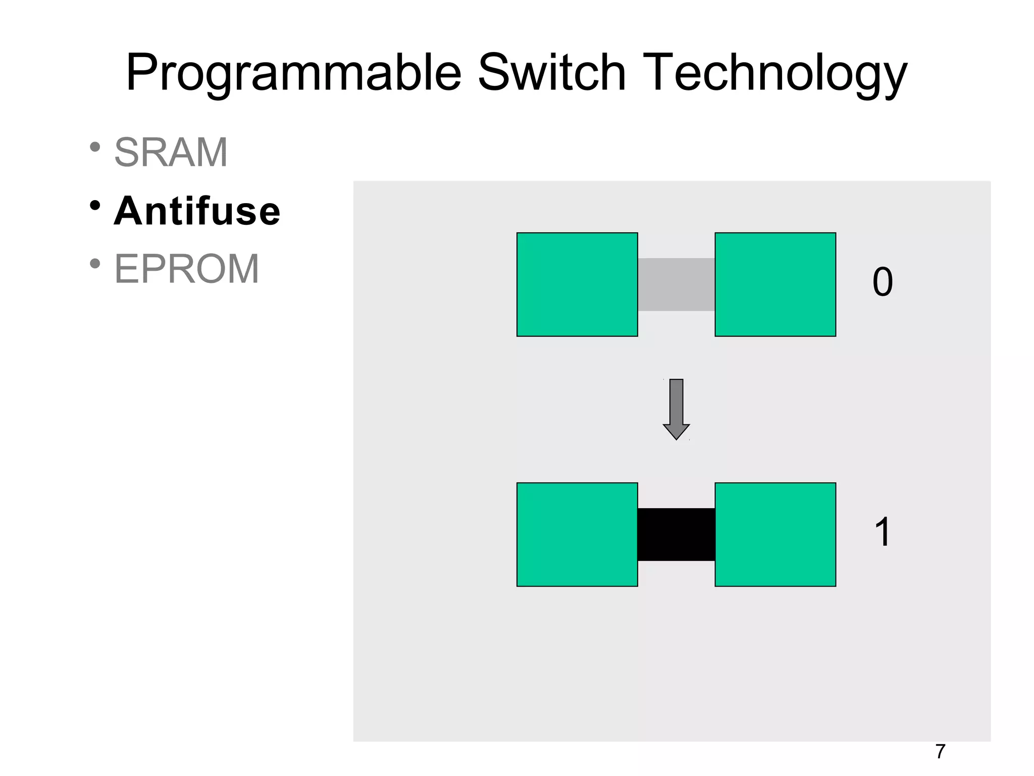
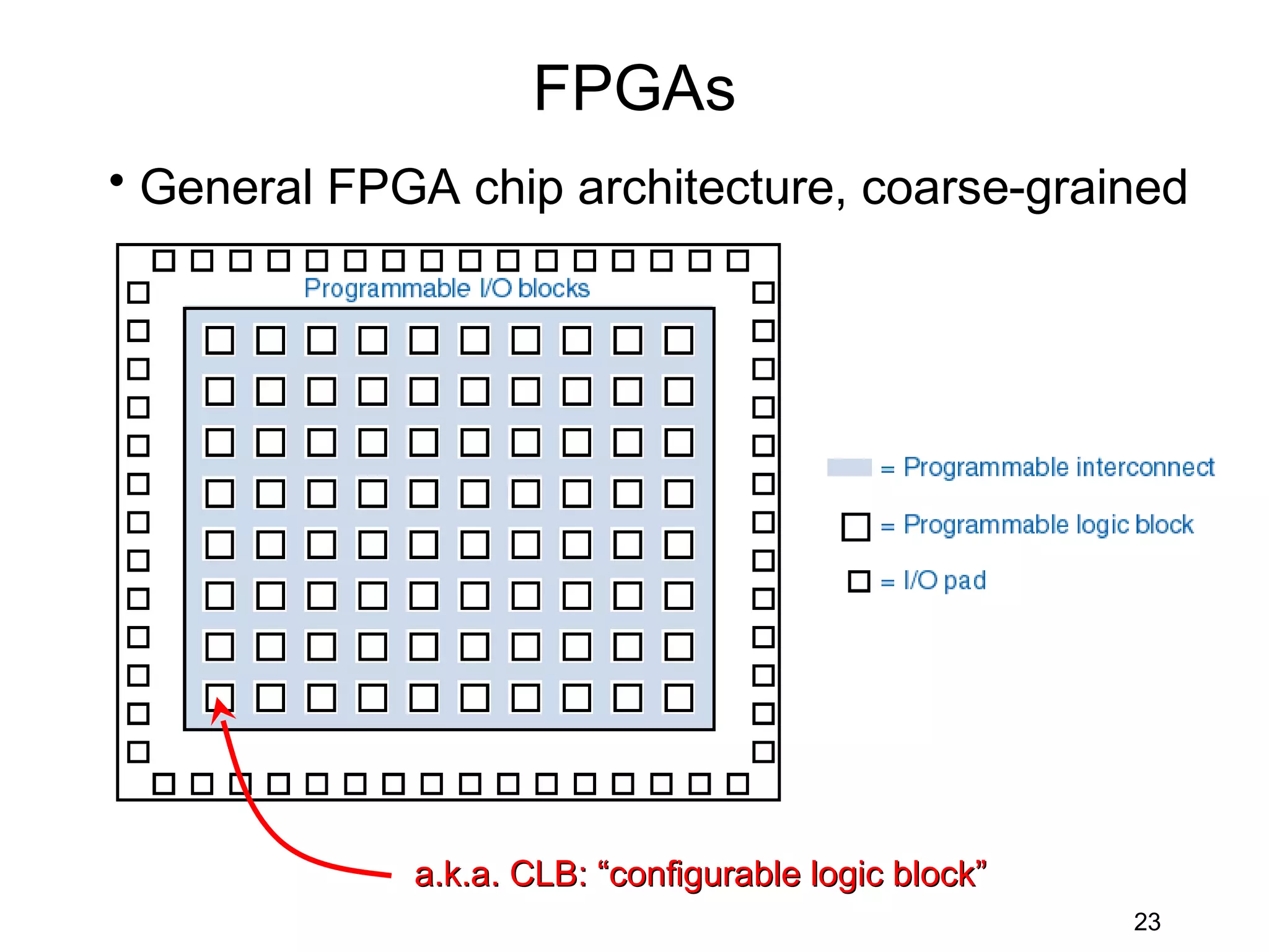
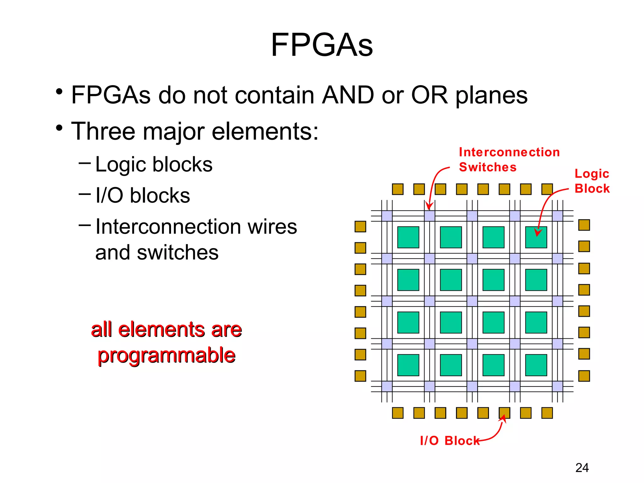
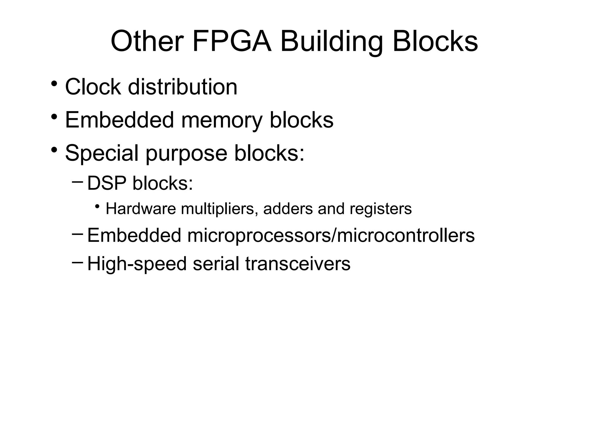
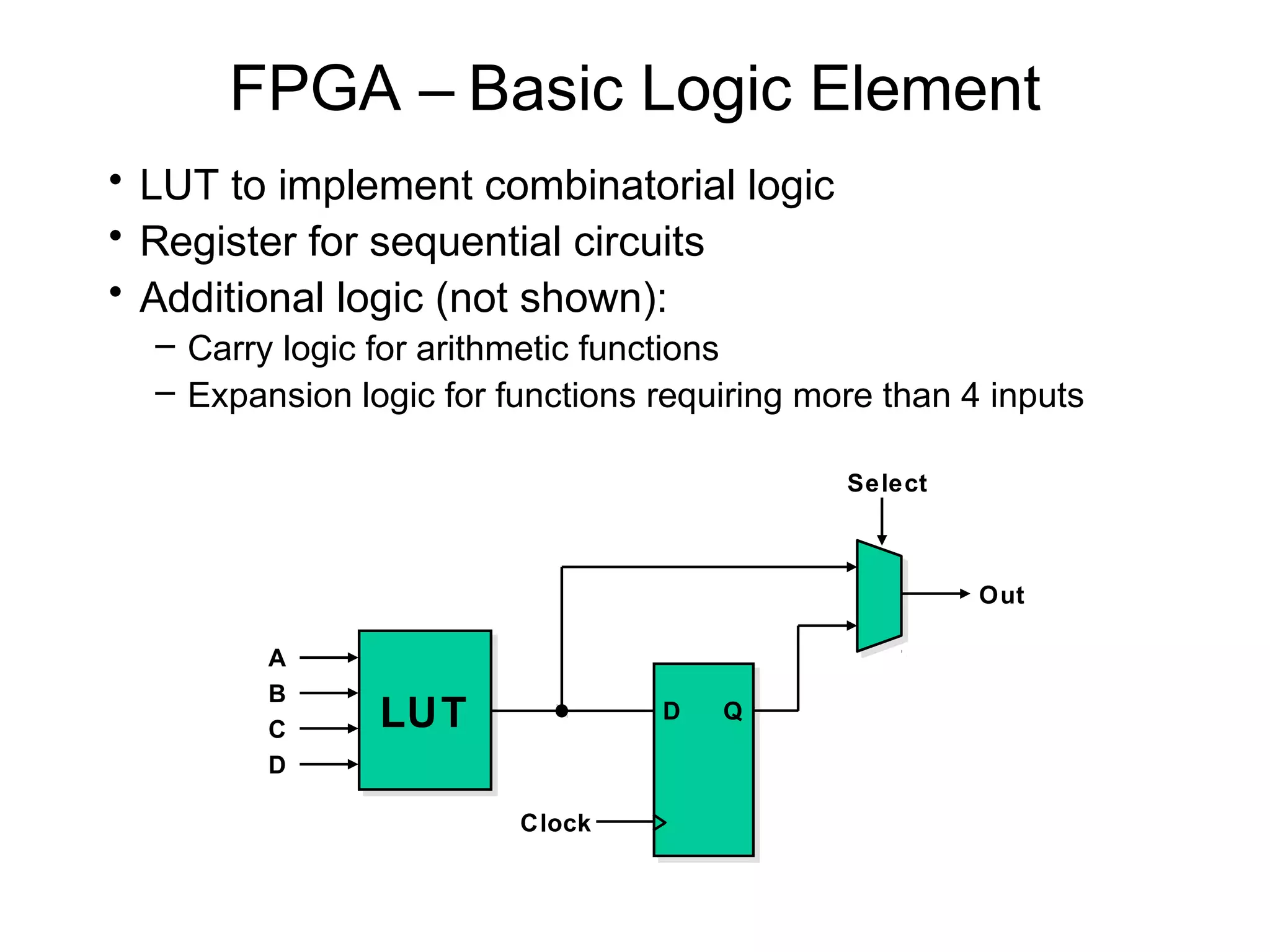
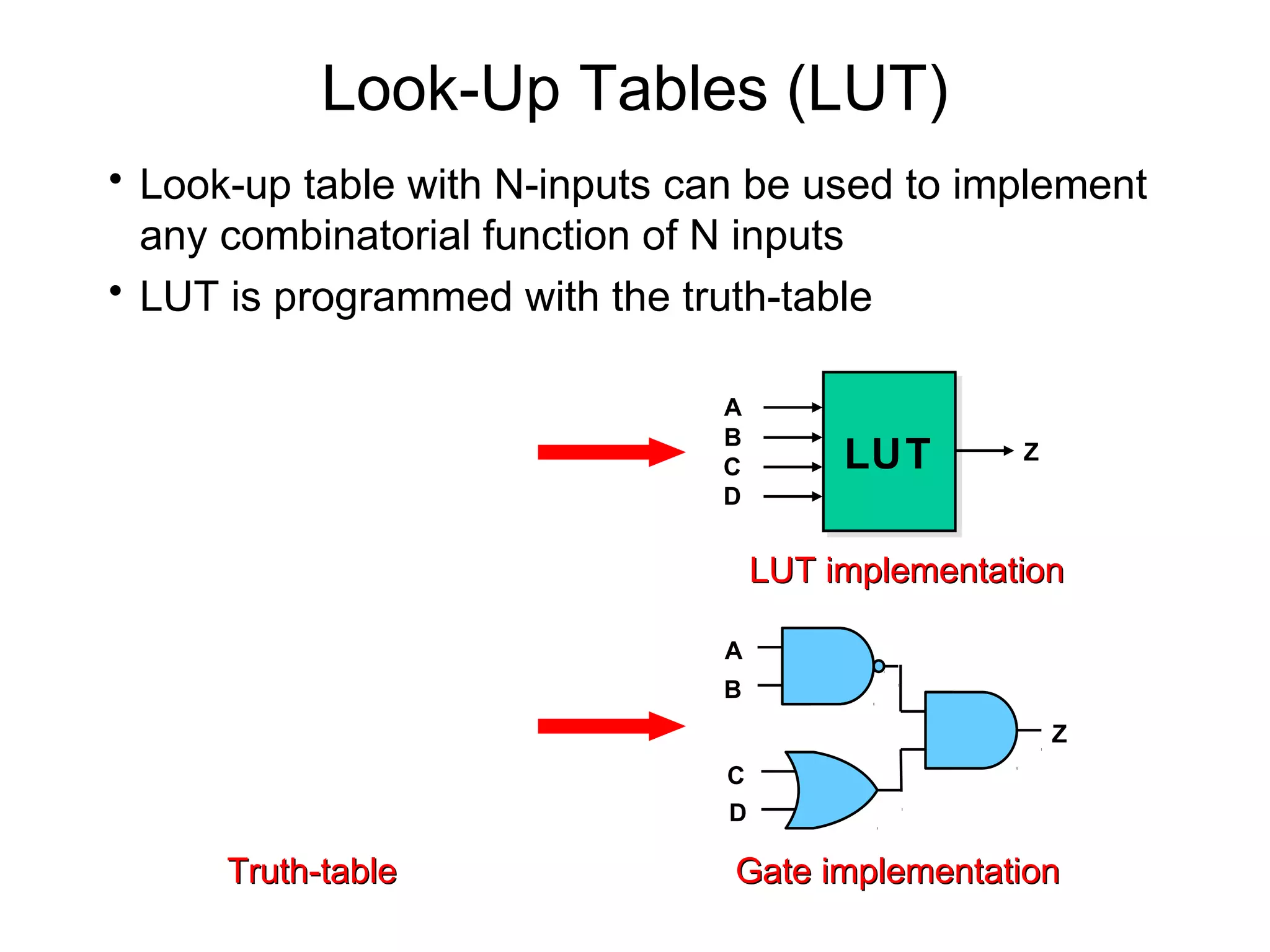
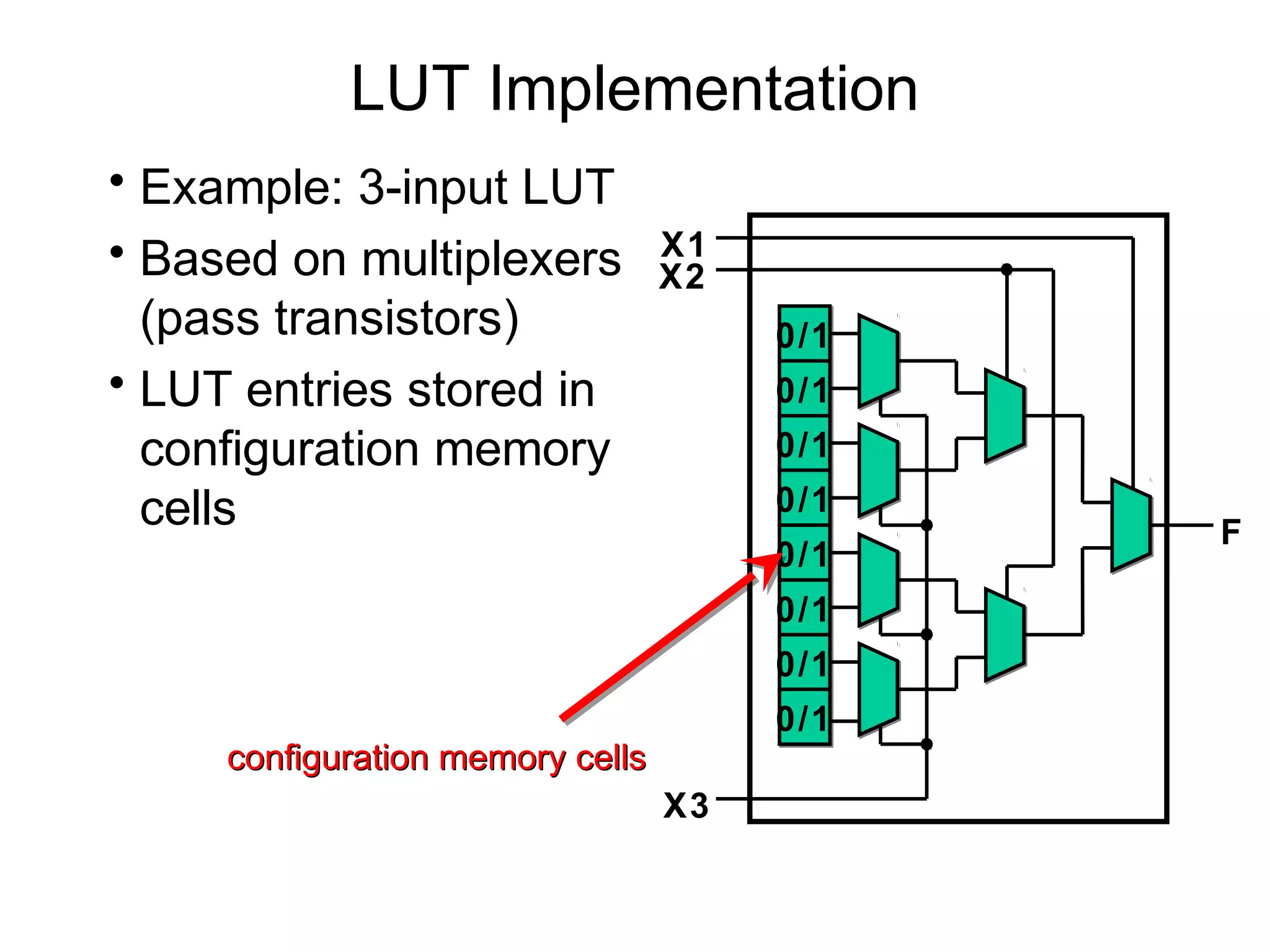

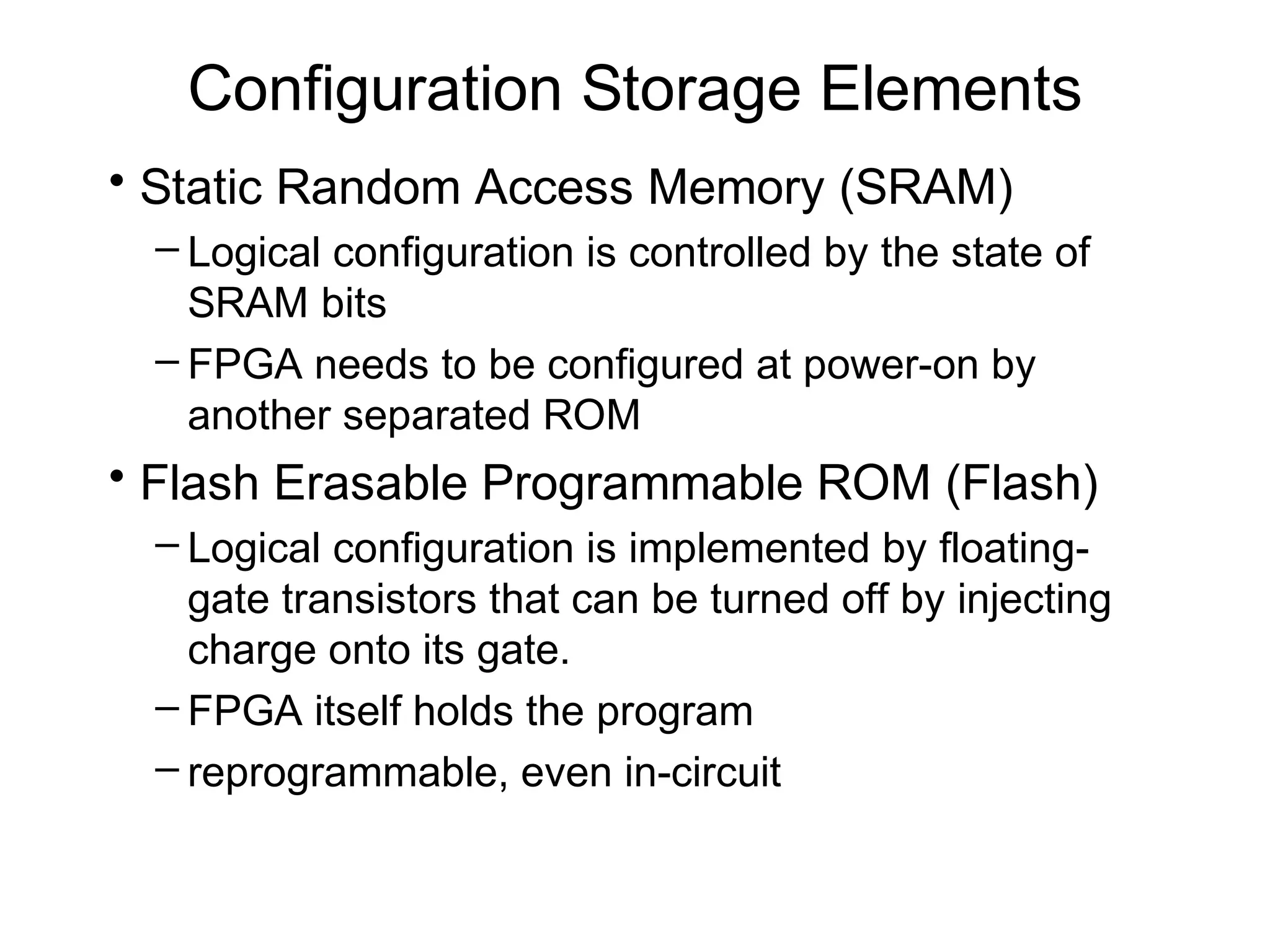
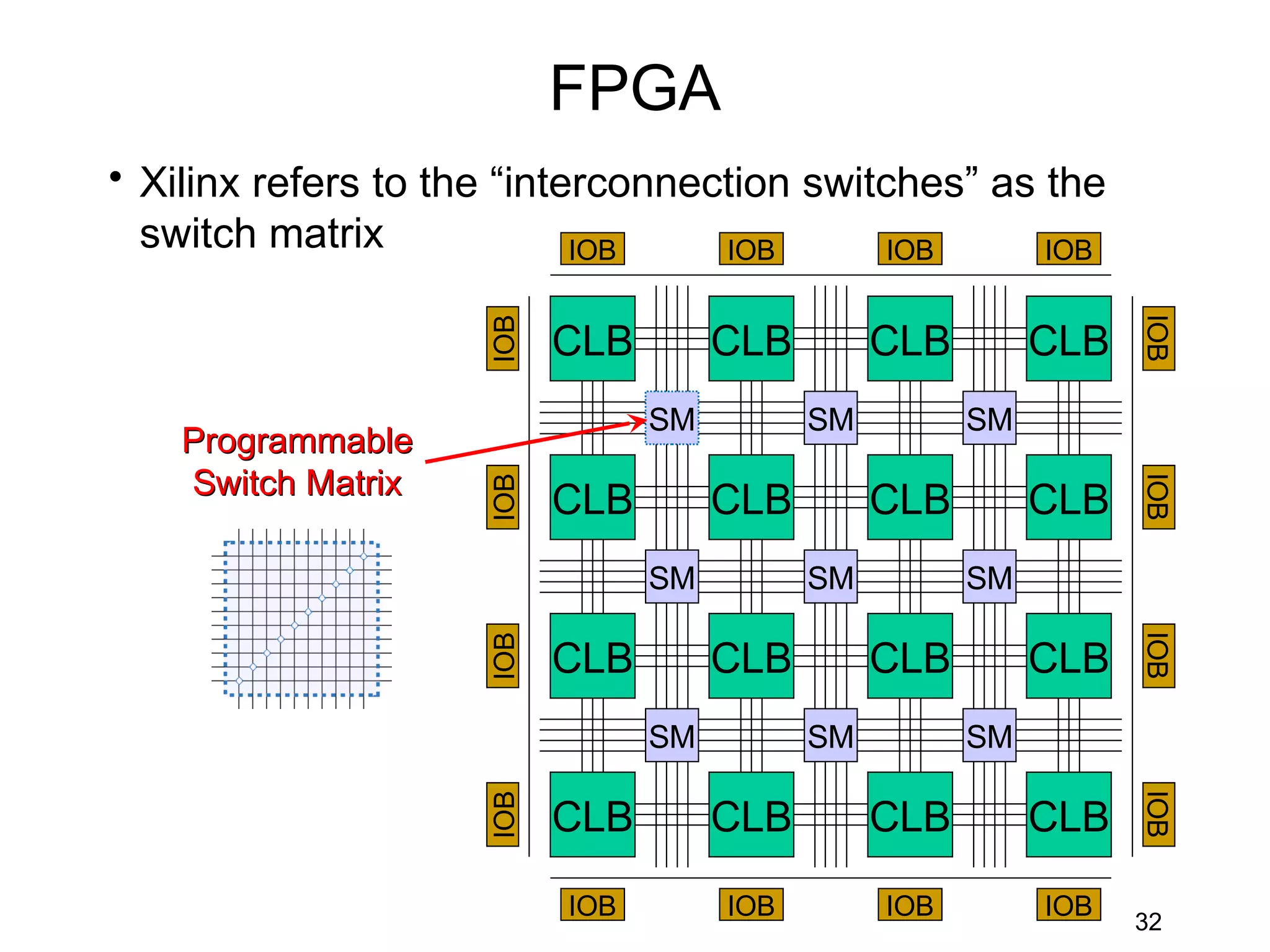
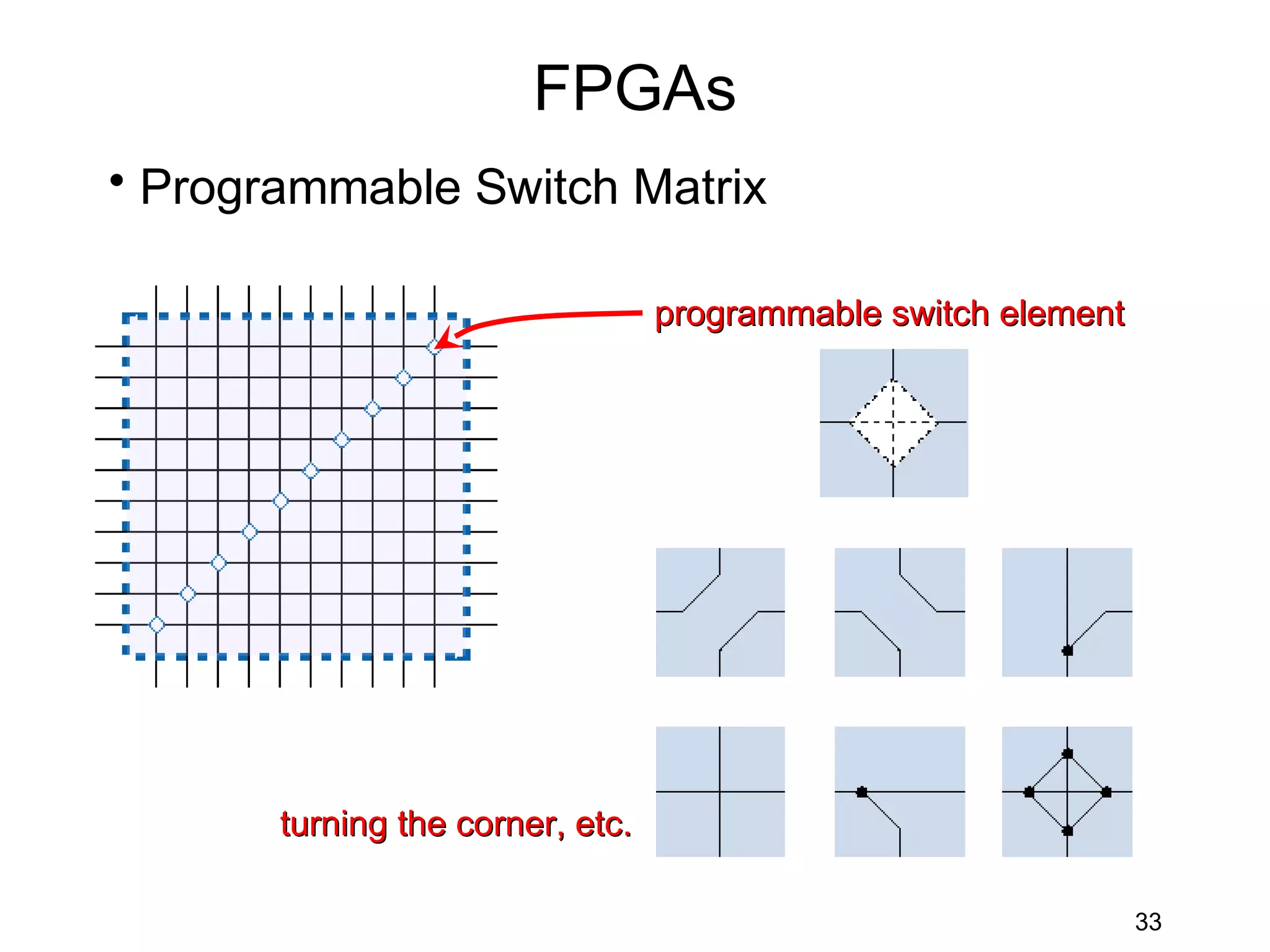
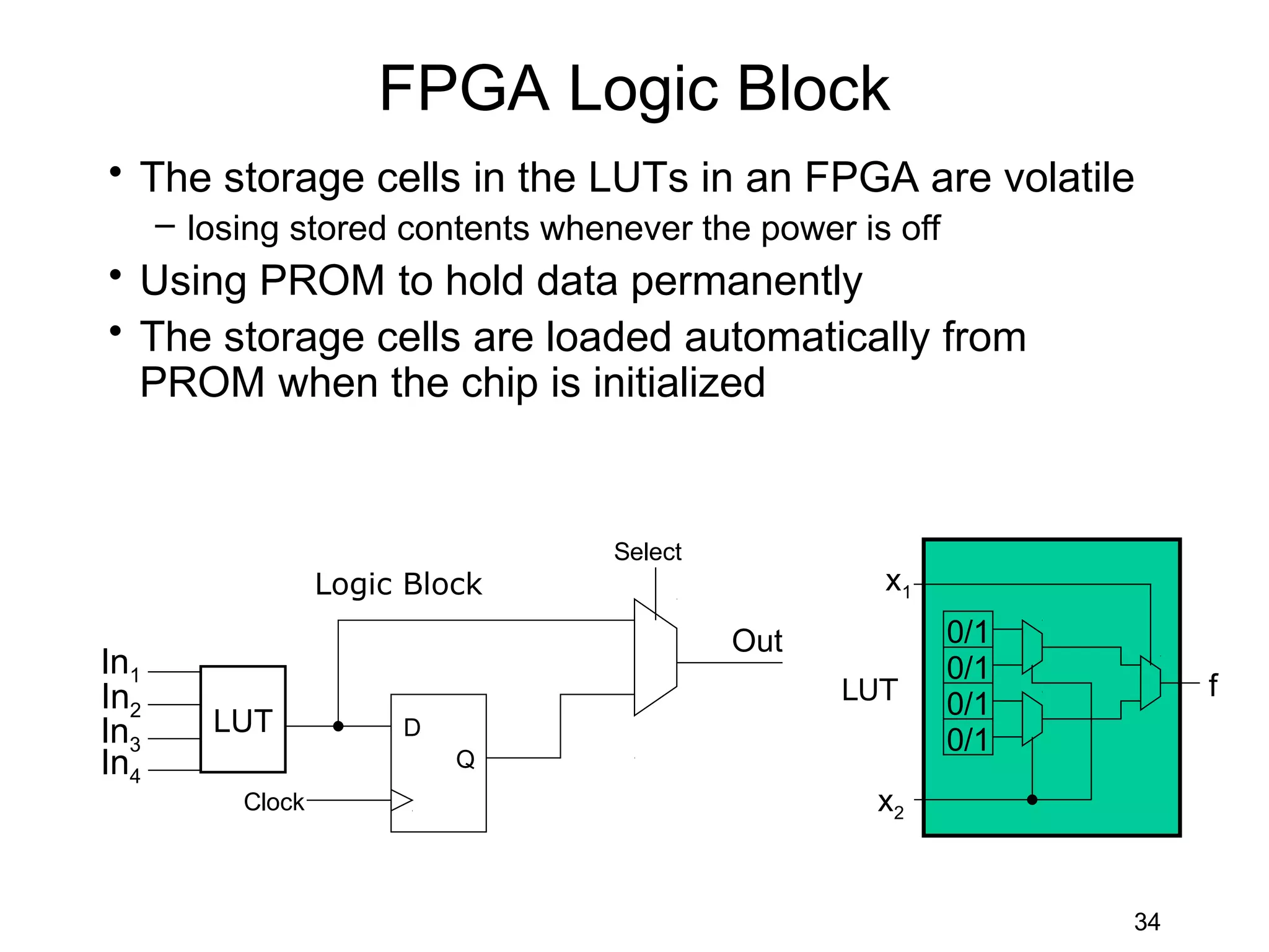
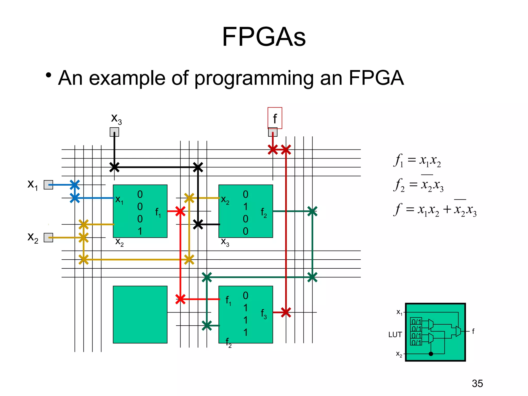
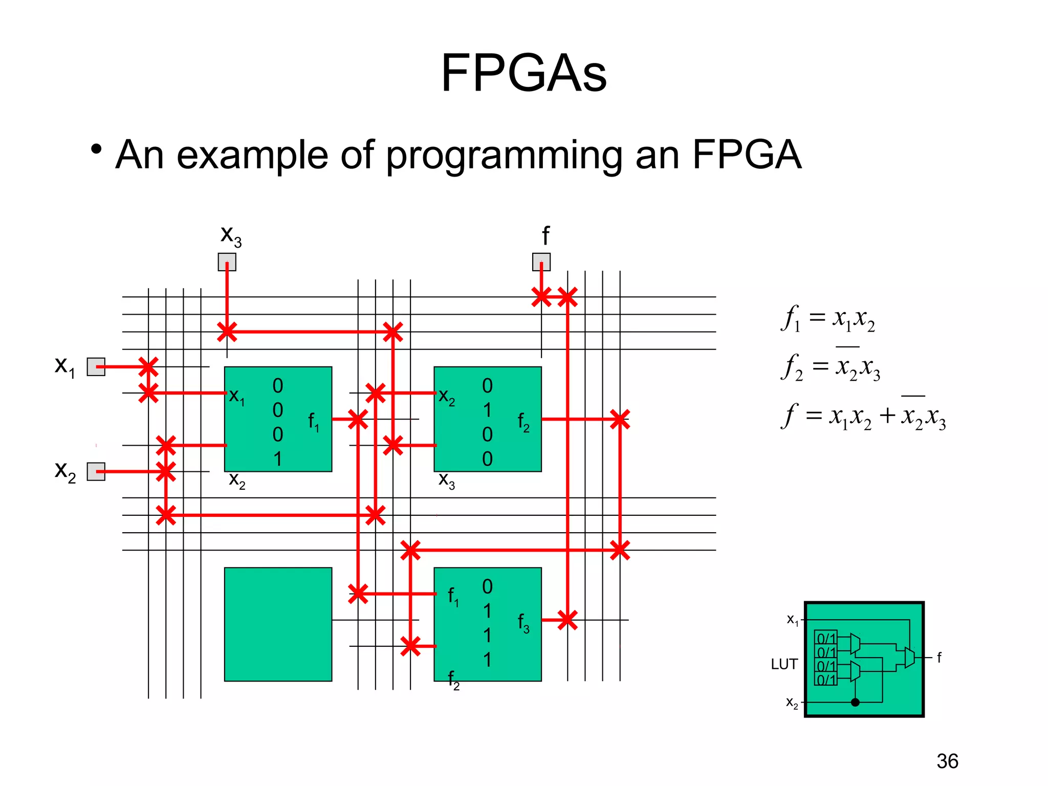
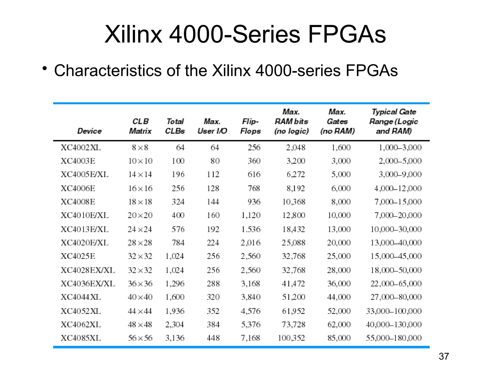
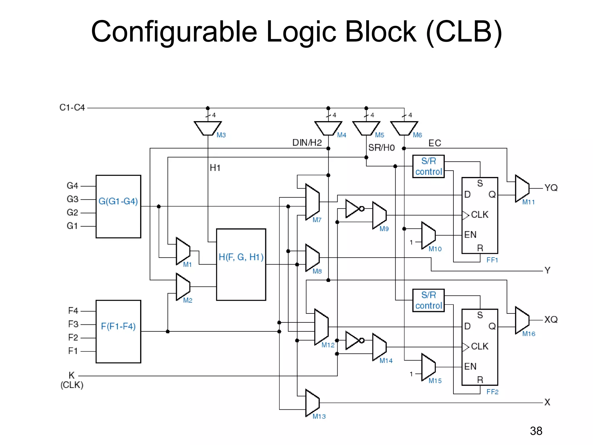
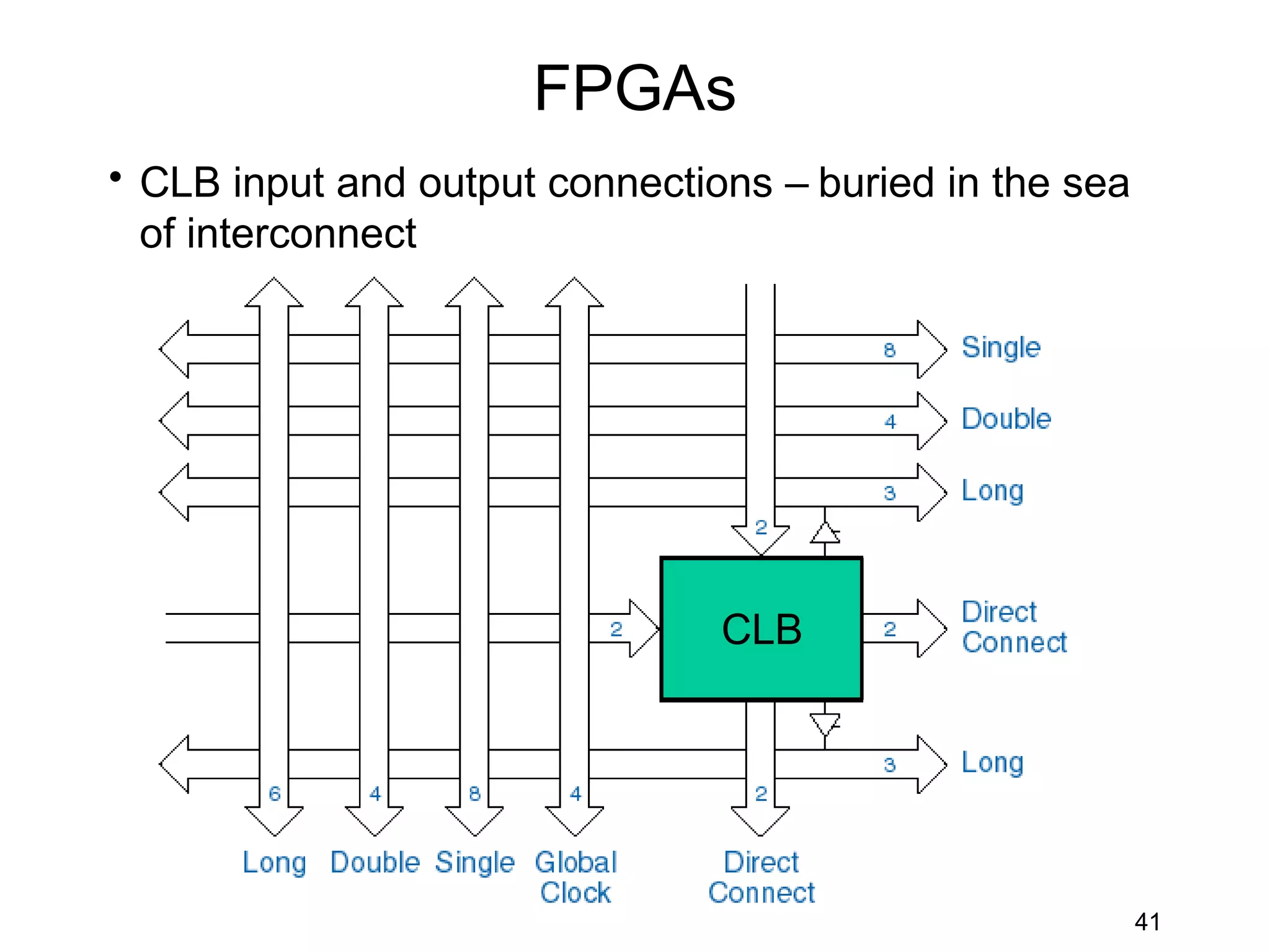
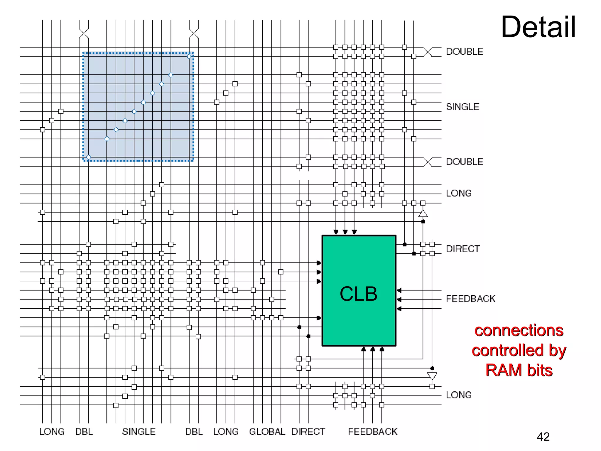
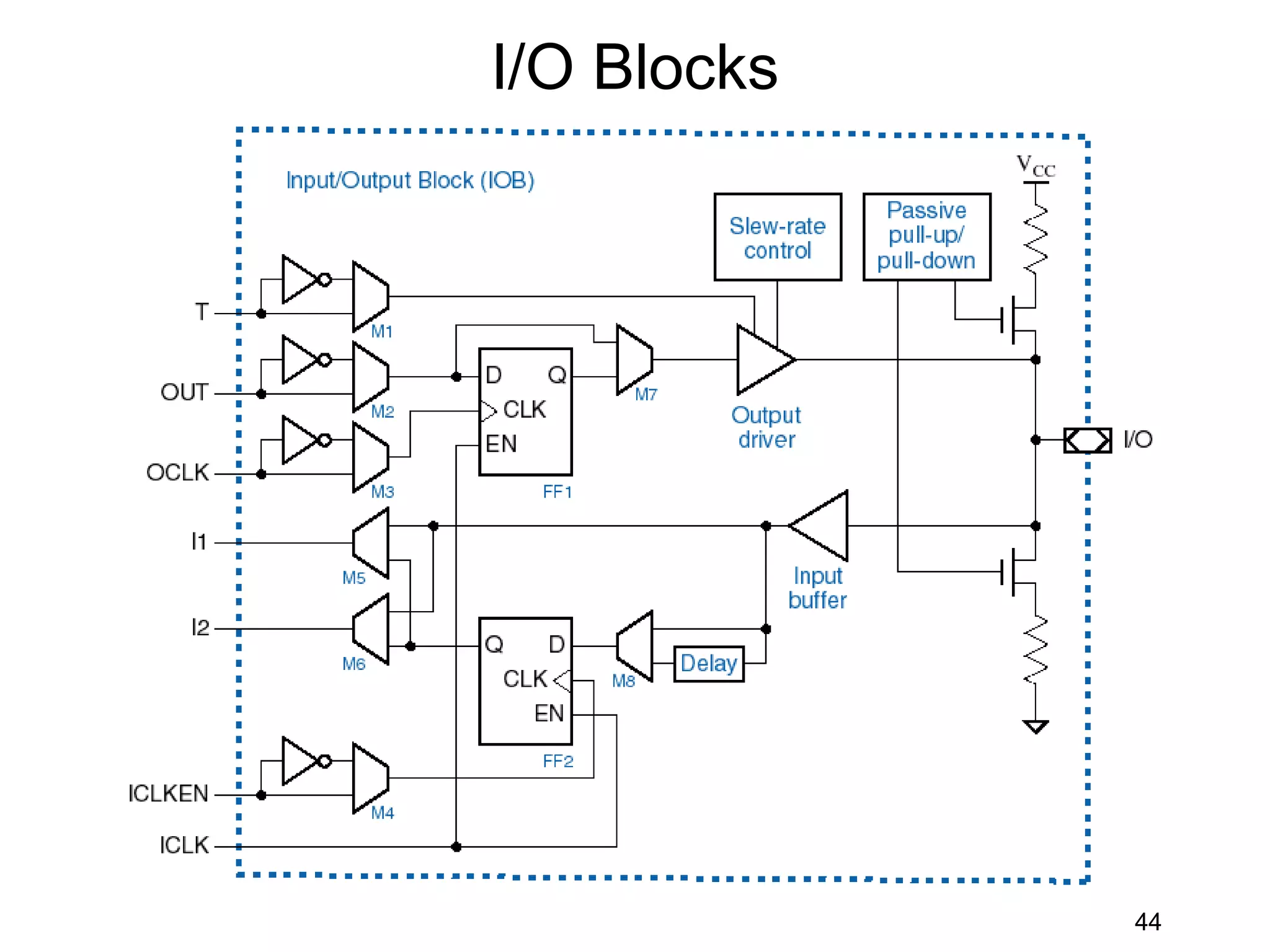
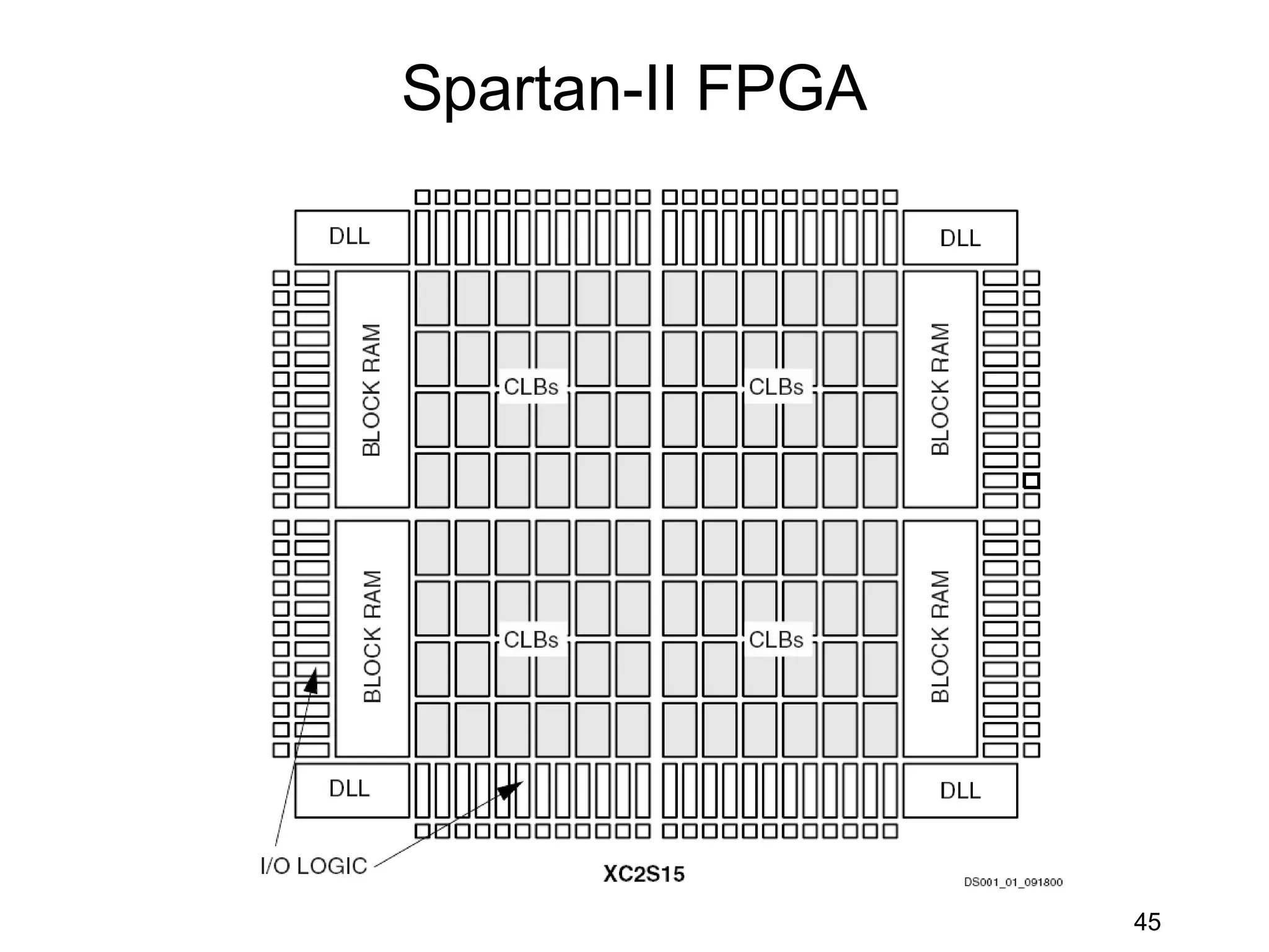
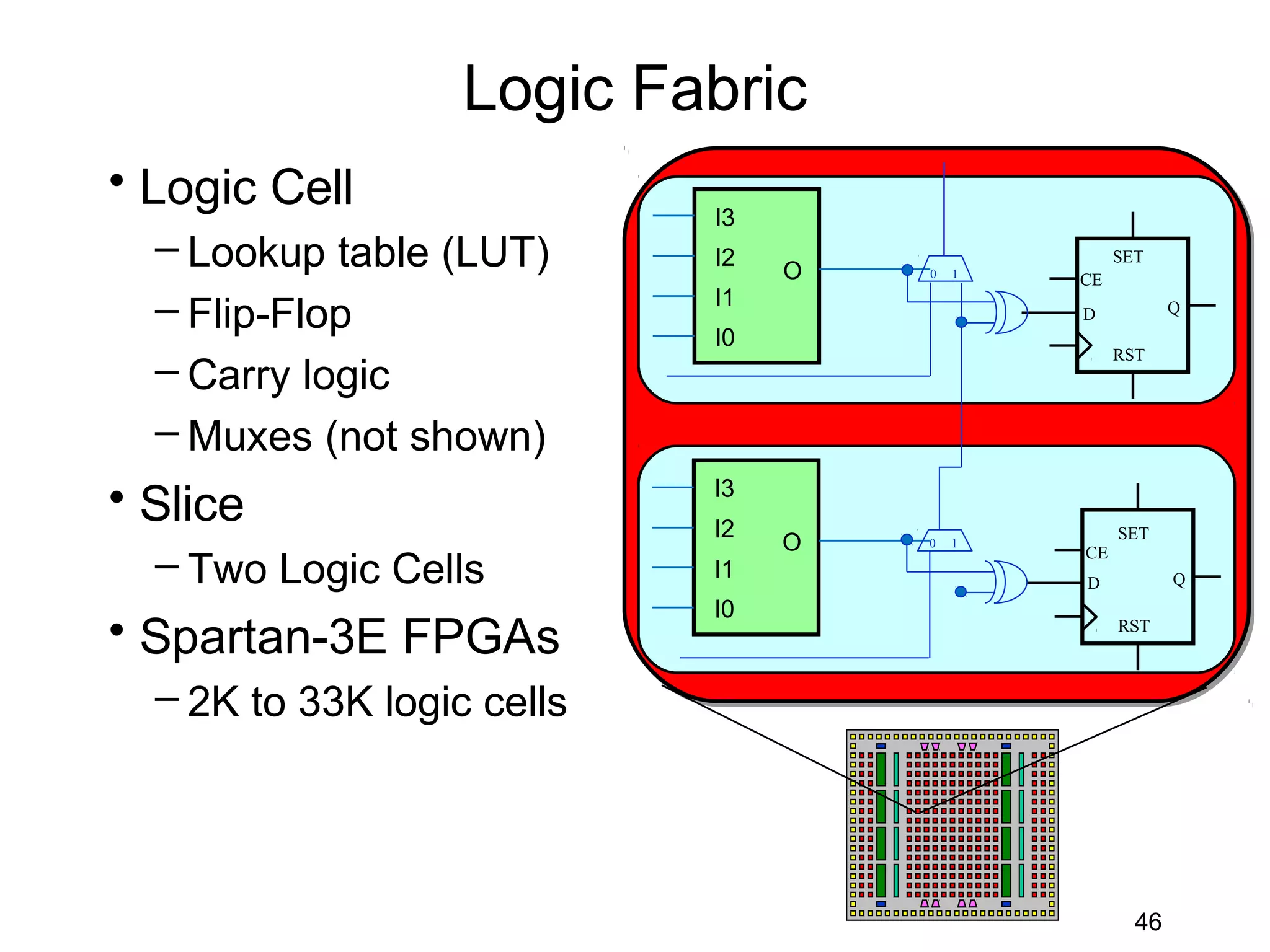
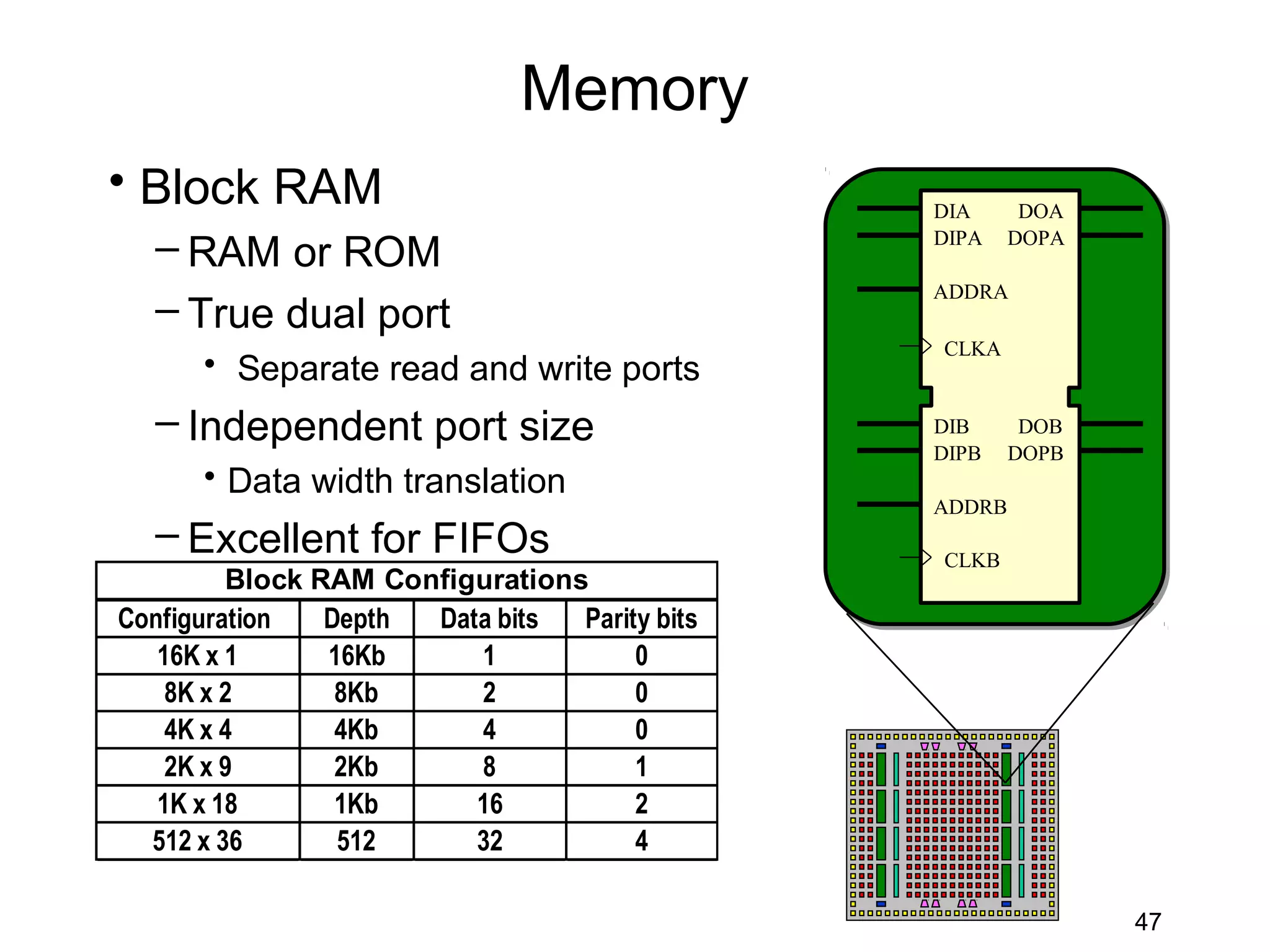
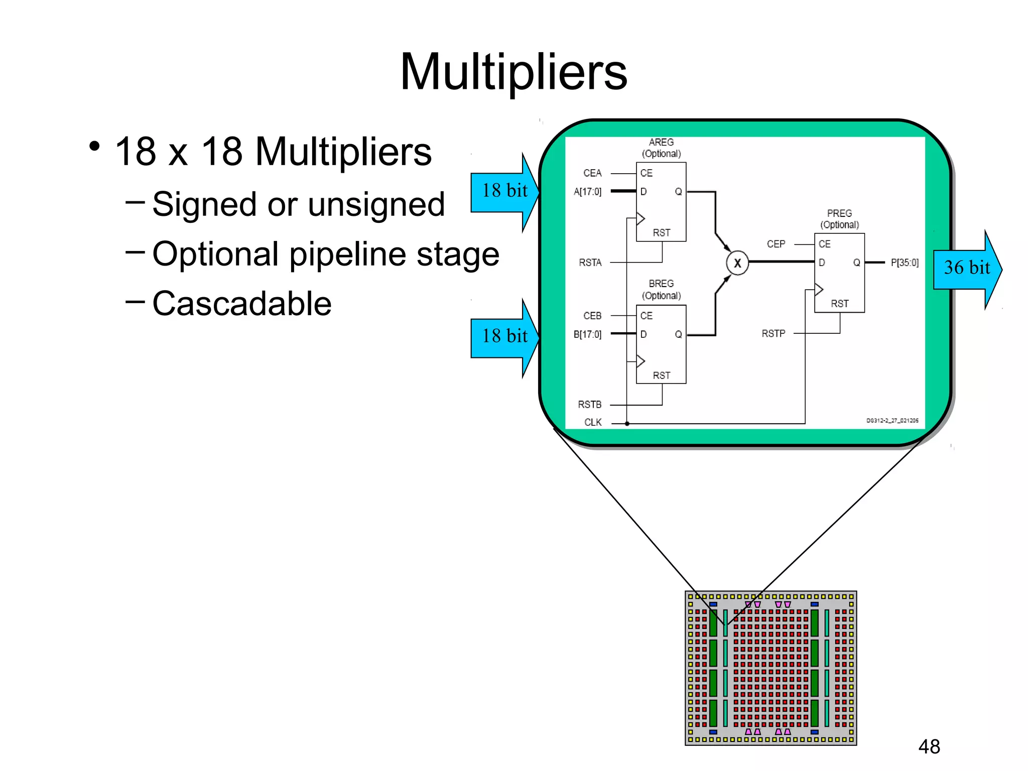
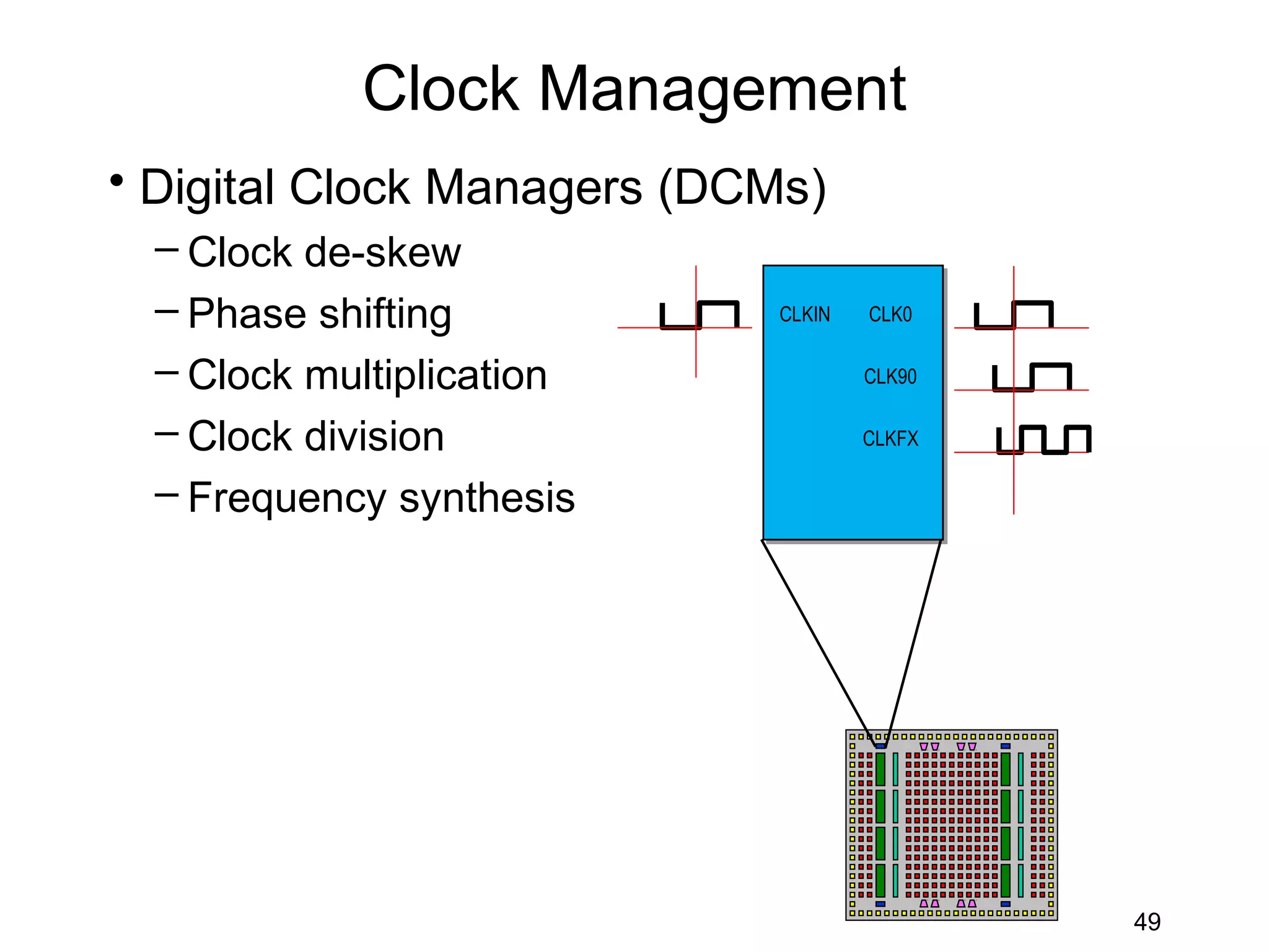
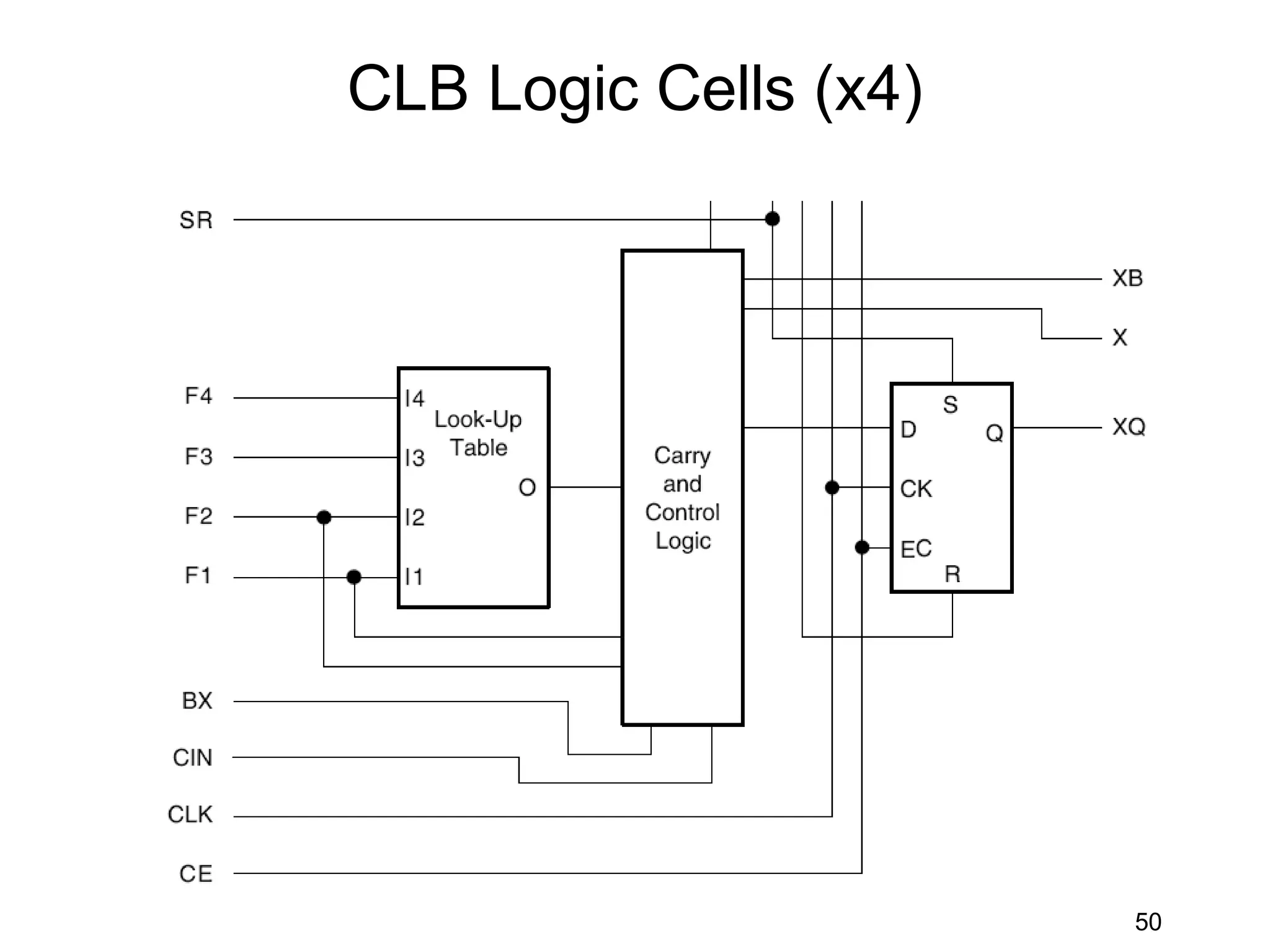
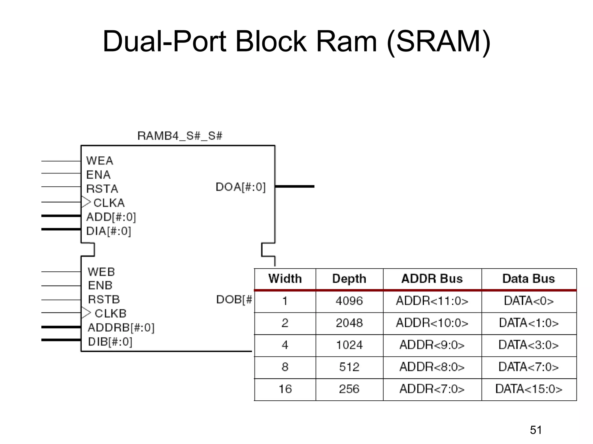
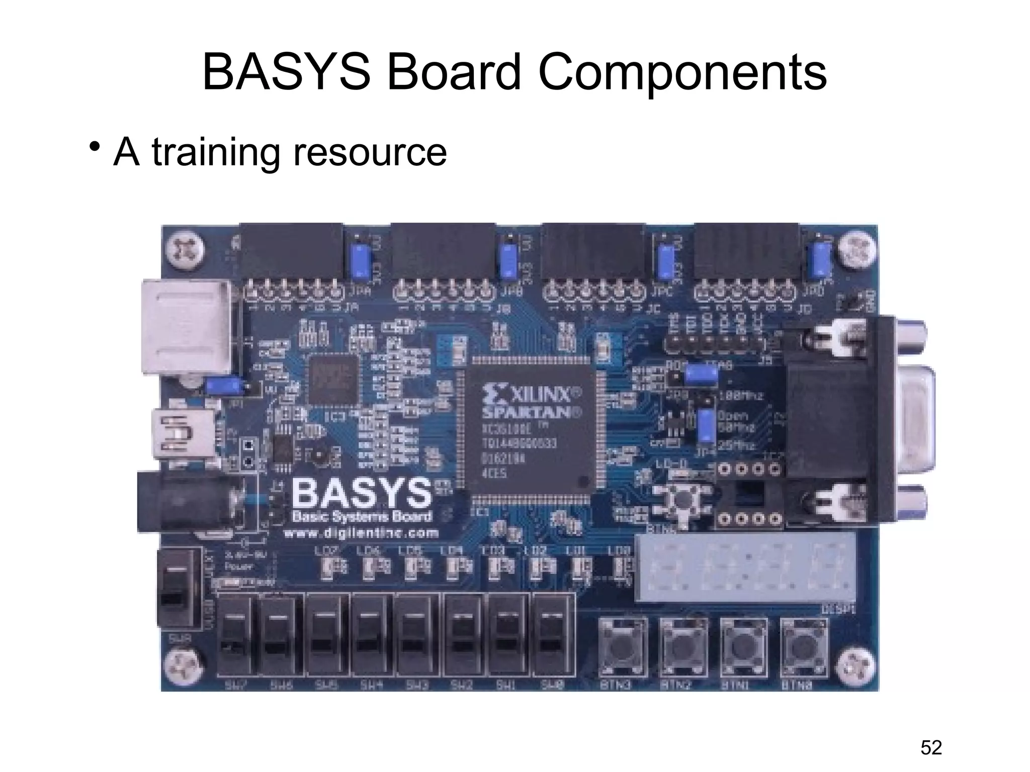
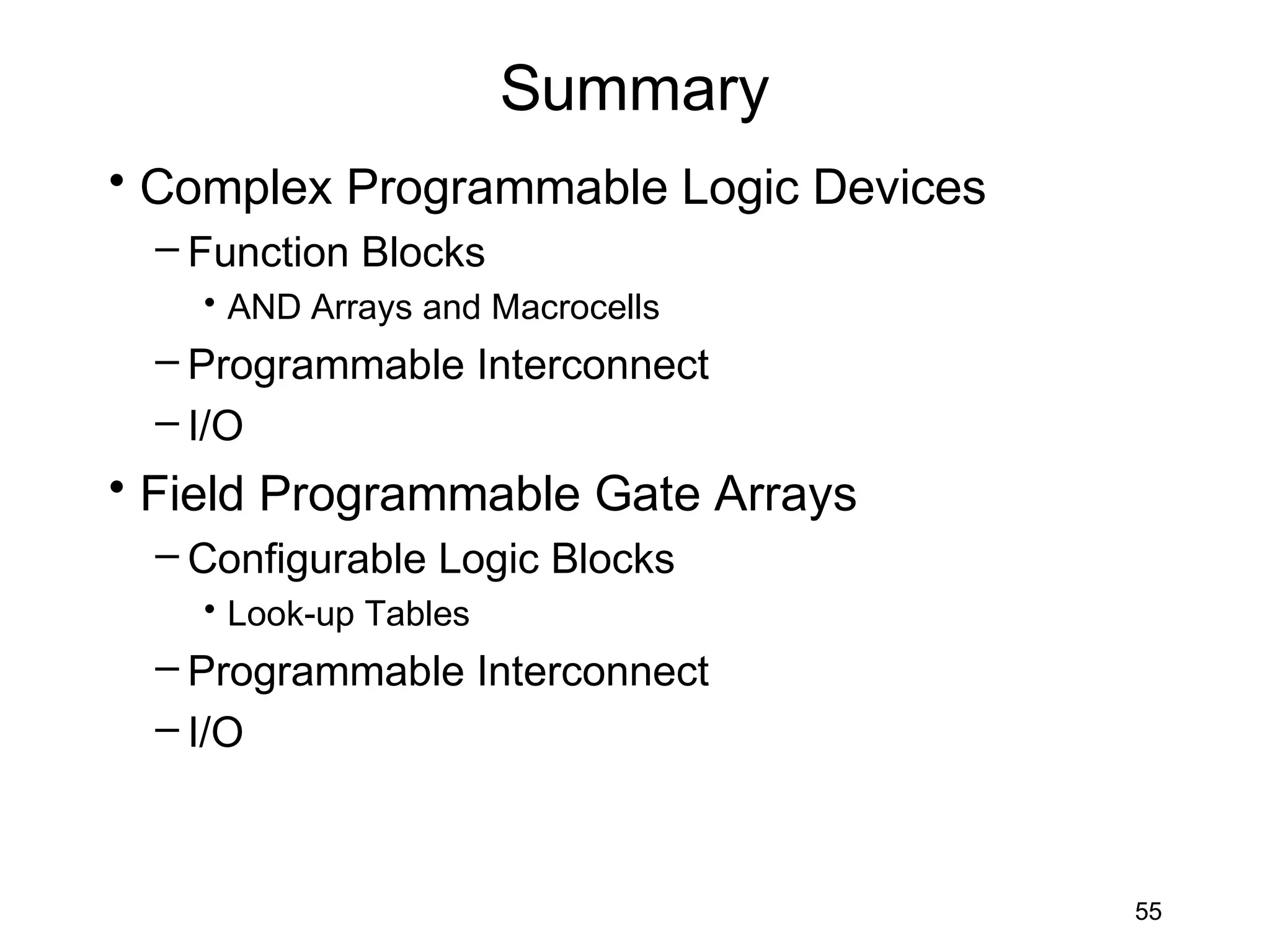

This document discusses field programmable gate arrays (FPGAs). It begins by describing FPGA basics and architecture, including configurable logic blocks (CLBs), I/O blocks, and switch matrices. It then discusses FPGA advantages such as low cost, fast prototyping, and reusability. The document also covers FPGA process technologies including SRAM, antifuse, and EPROM/EEPROM/Flash. It provides details on FPGA architectures, logic elements, routing, memory blocks, and examples of Xilinx FPGAs.