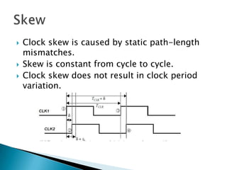
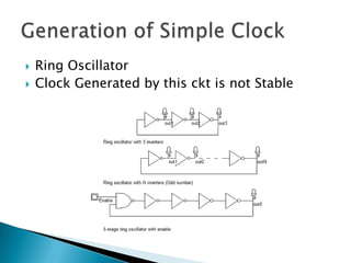
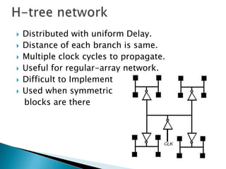
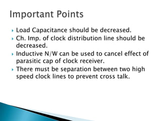
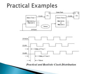
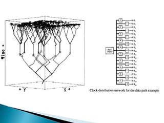
3. Introduction Ideally Minimum Rise time & Fall time Specified Duty Cycles Zero Skew In Practical Considerable Rise time and Fall Time Duty Cycle can also very Non Zero Skew Jitter
4. Clock skew is caused by static path-length mismatches. Skew is constant from cycle to cycle. Clock skew does not result in clock period variation. Skew
5. Clock period can reduce or expand on a cycle-by-cycle basis. It is strictly a temporal uncertainty measure and is often specified at a given point on the chip. Jitter directly impacts the performance of a sequential system. Jitter
7. For high performance clk we required separate clock chip which use crystal Oscillator. Pierce Crystal Oscillator
8. VLSI chip receives one or more primary clock signals. Many time we require two non-overlapping signals. Generation Of Non-Overlapping Signal
9. H-tree network Distributed with uniform Delay. Distance of each branch is same. Multiple clock cycles to propagate. Useful for regular-array network. Difficult to Implement Used when symmetric blocks are there
10. Route main signals to each macro block. Use clock decoders to carefully balance the delays. Clock decoder will generate different phase signals which are required for different macro block. Clock Decoder
11. If we want to handle large fanout loads then clock signal must be buffered. There may be possiblity that we get phase errors and different clock skew at each o/p. Buffer
12. Here we are cross connecting all buffer lines. Clock skew and phase problem is eliminated. It is important that every buffer stage drives the same number of fanout gates. Buffer and Cross Connections
13. Load Capacitance should be decreased. Ch. Imp. of clock distribution line should be decreased. Inductive N/W can be used to cancel effect of parasitic cap of clock receiver. There must be separation between two high speed clock lines to prevent cross talk. Important Points