Downloaded 115 times
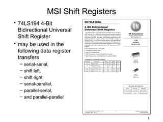
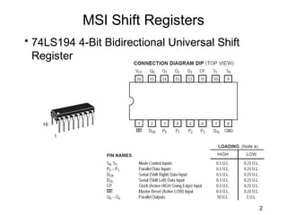
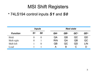
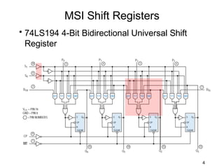
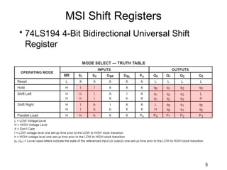
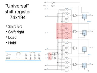
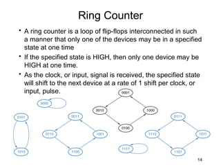
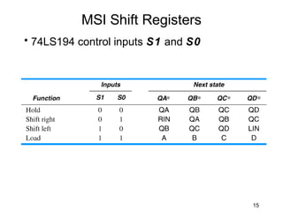
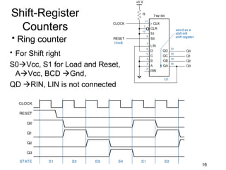
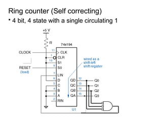
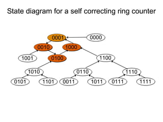
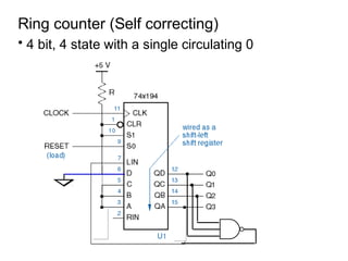
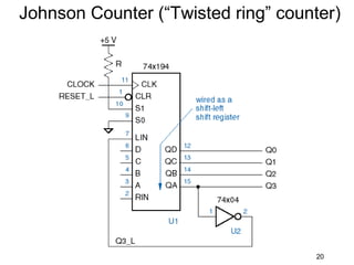
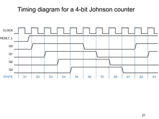
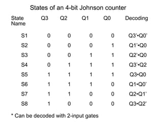
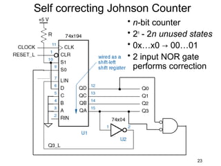
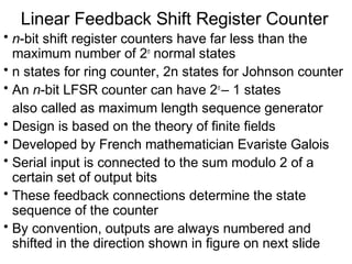
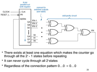
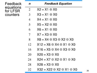
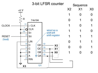
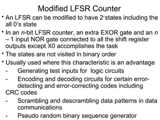
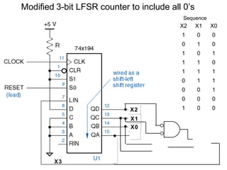

The document discusses various types of shift registers including the 74LS194 4-bit bidirectional universal shift register which can perform shift left, shift right, serial-serial, serial-parallel, parallel-serial, and parallel-parallel transfers. It also describes ring counters, Johnson counters, and linear feedback shift register (LFSR) counters. LFSR counters can cycle through all possible 2^n-1 states using feedback connections to determine the state sequence.