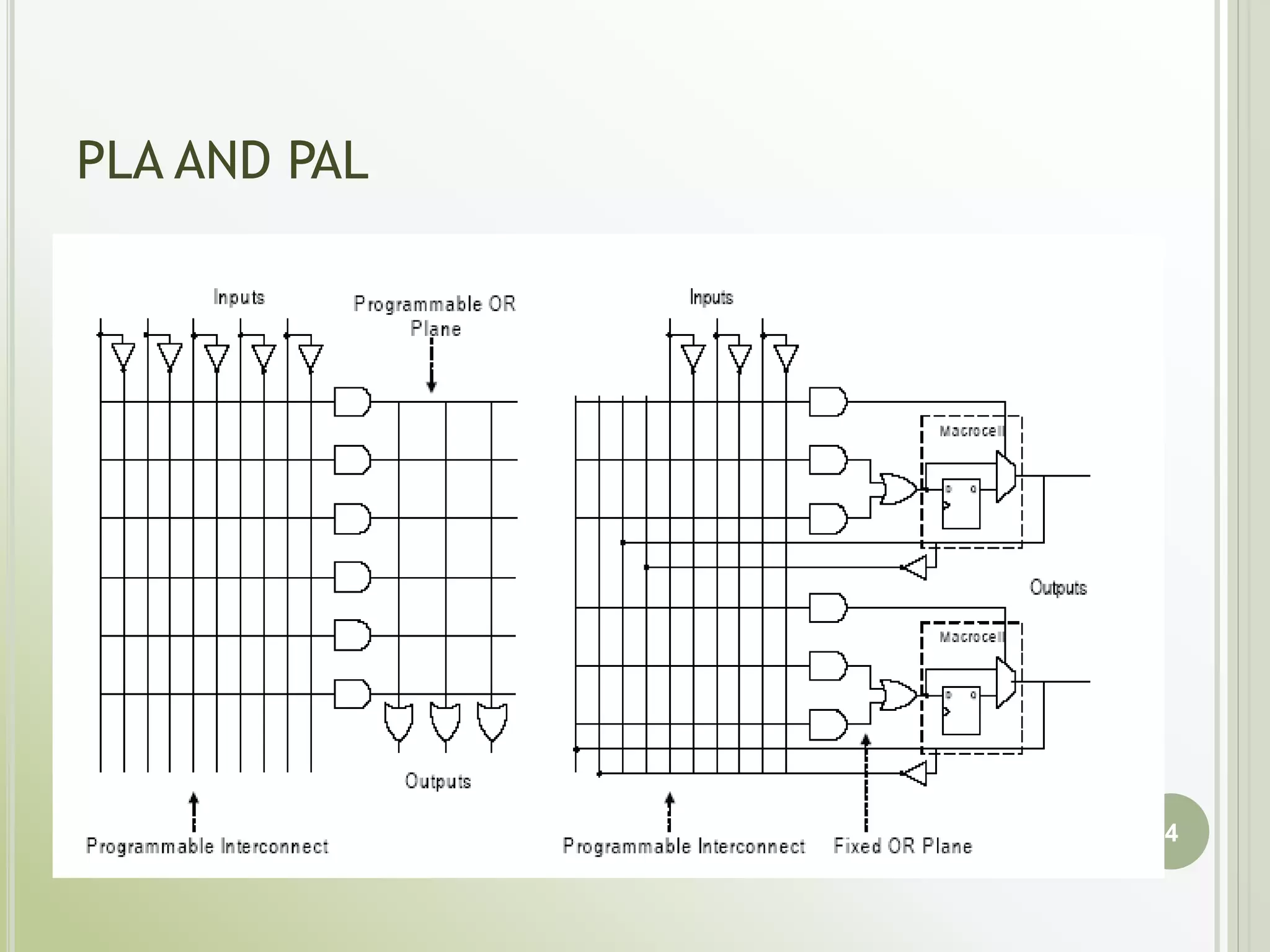
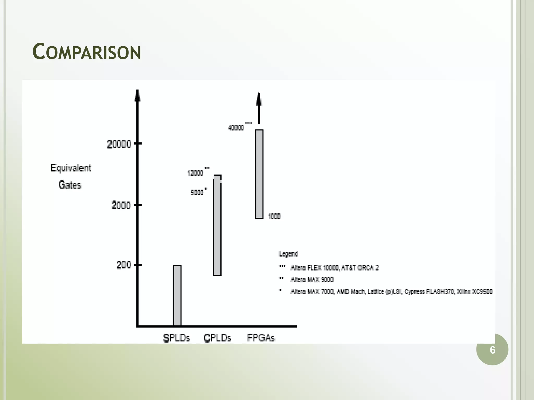
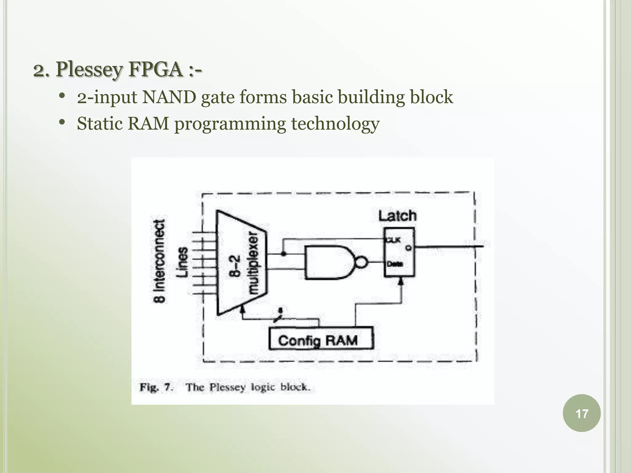
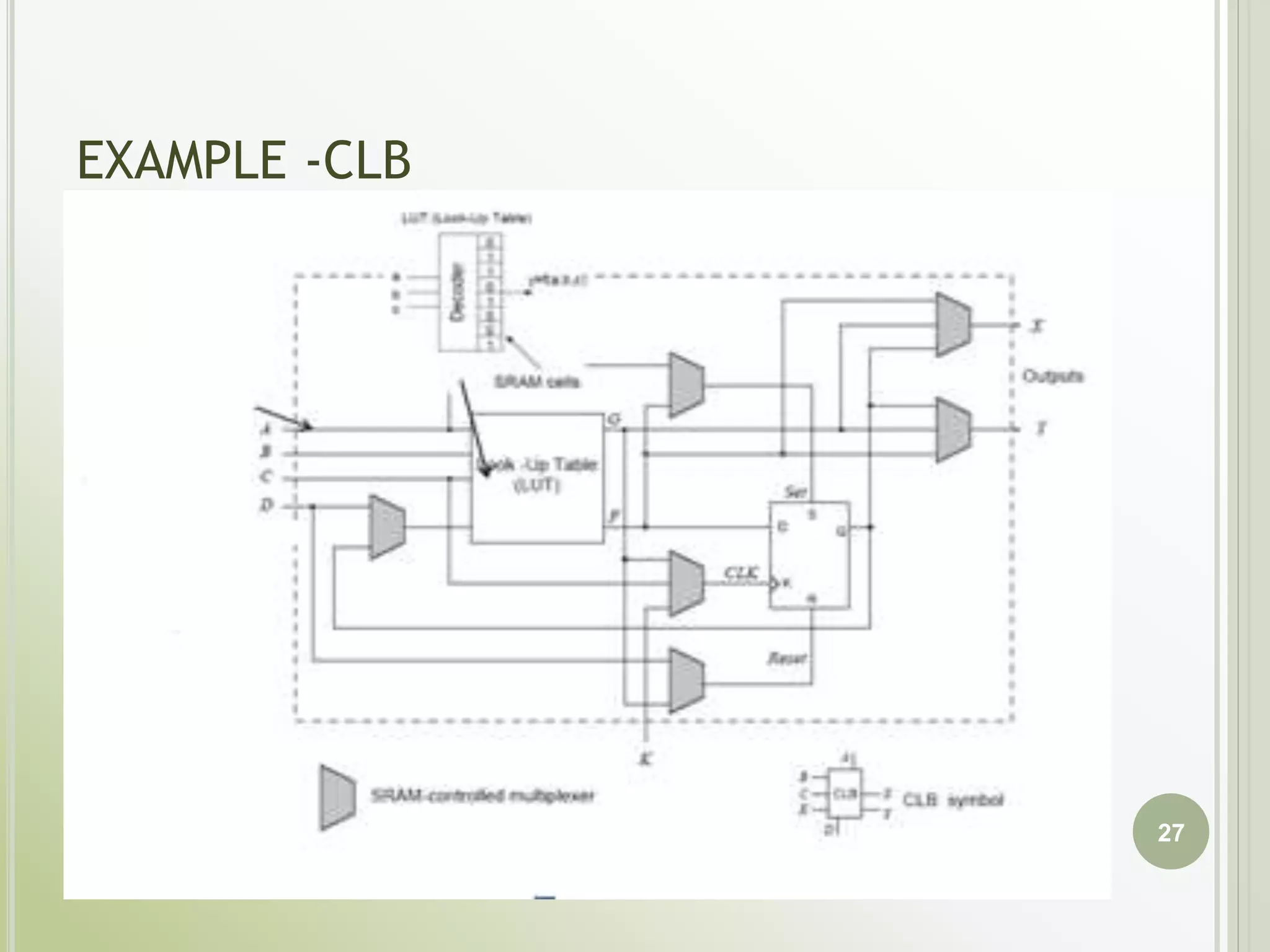
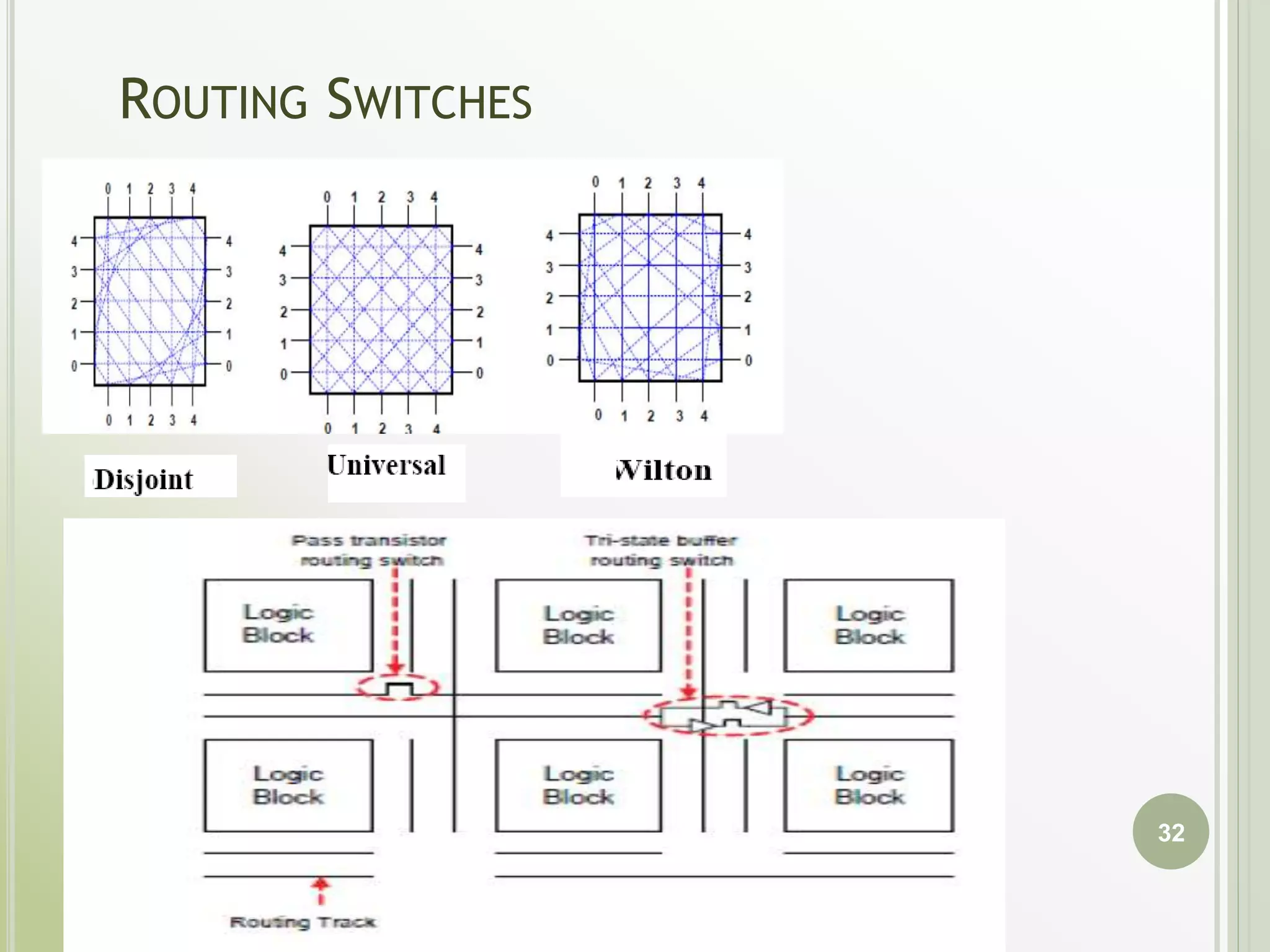
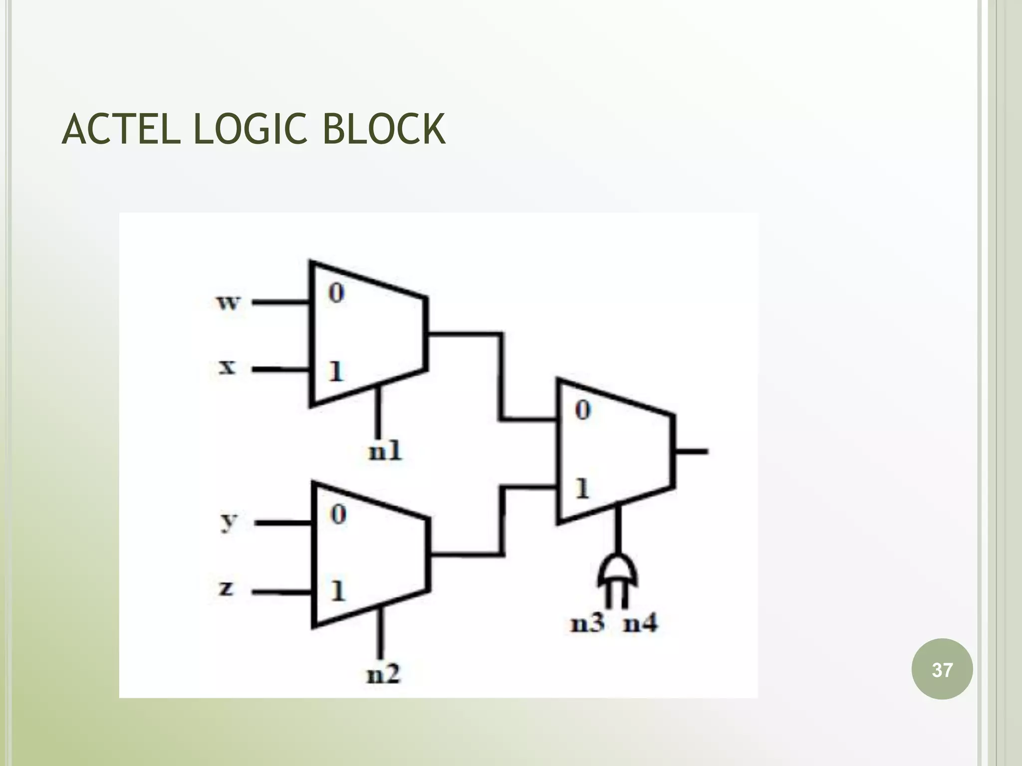
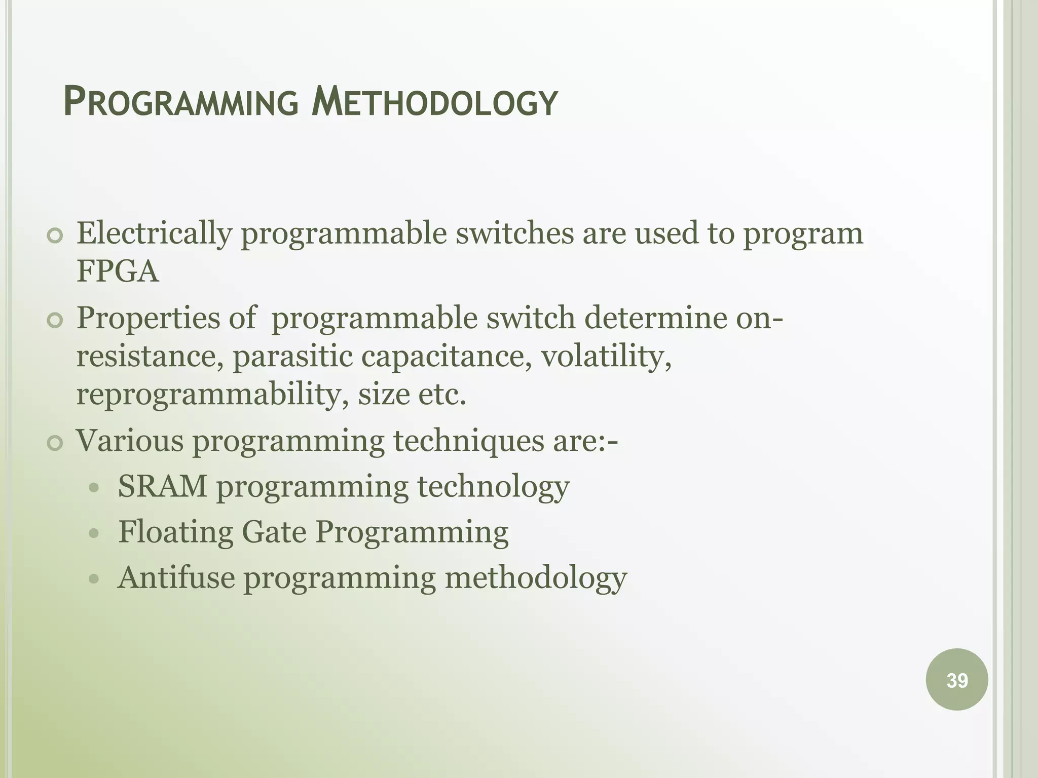
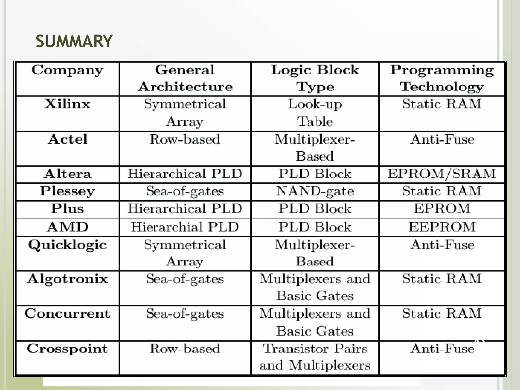
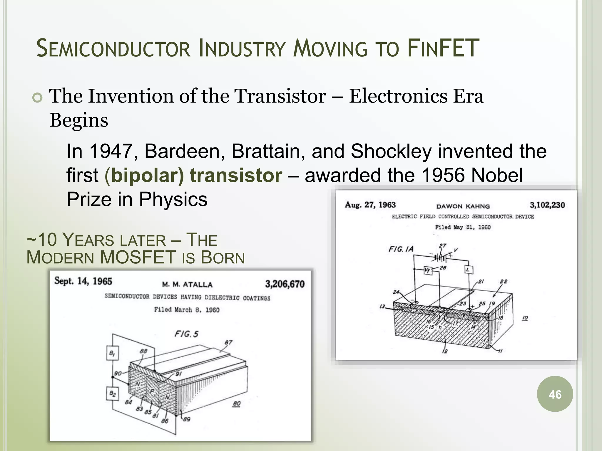
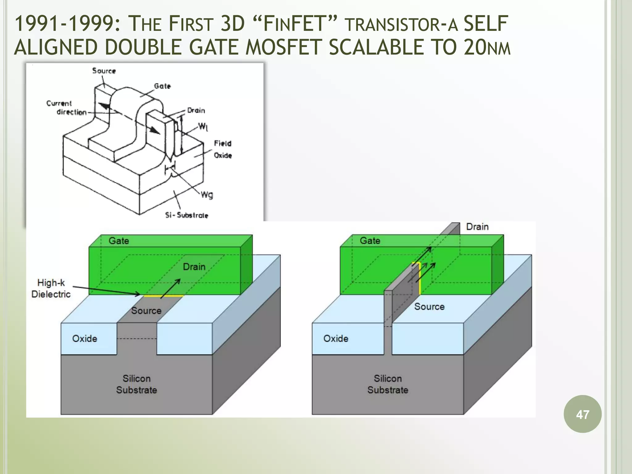
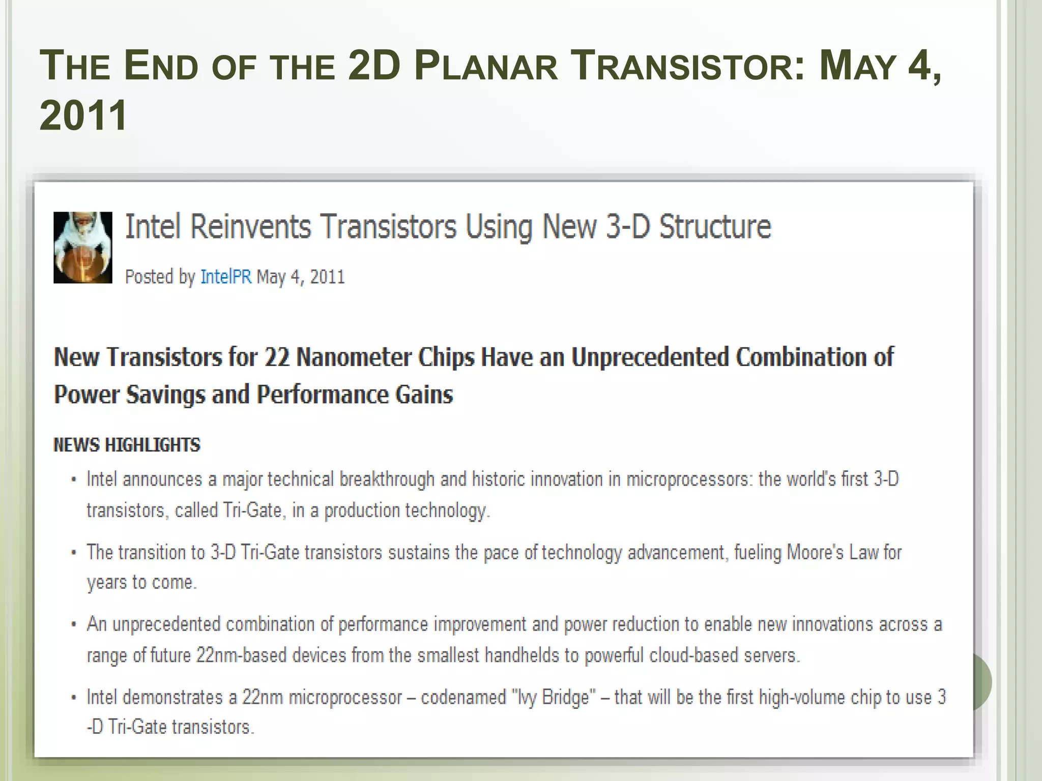
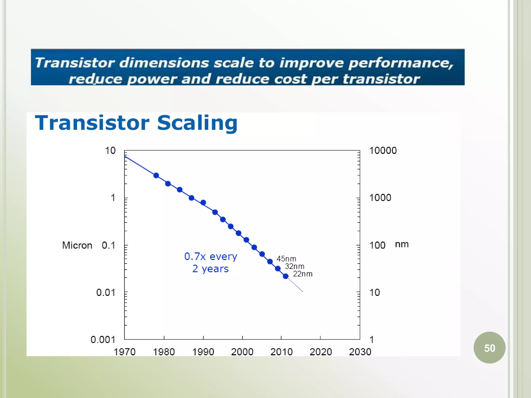
FPGA AND ITS LOW POWER
TECHNIQUE
(FIELD PROGRAMMABLE GATE ARRAY)
Presented by :
Dr.D.RUKMANIDEVI
PROFESSOR
R.M.D.ENGINEERING COLLEGE
1
HISTORY
Programmable Read Only Memory (PROM)-1970
 fuse programming
 n- address i/p can implement n i/p logic fun.
Problem:
 Area efficiency.
Programmable Logic Array (PLA)-1977
 Programmable AND plane followed by
programmable or wired OR plane.
 Sum of product form
Problem :
 Two level programming adds delay
2
NEXT -
Programmable Array Logic (PAL)-1977
 Programmable AND plane and fixed OR plane.
 Flexible comparably.
All these PLA and PAL are Simple Programmable
Logic Devices (SPLD).
Problem:
 Logic plane structure grows rapidly with number of
inputs
3
PLA AND PAL
4
NEXT -
To mitigate the problem
Complex Programmable Logic Devices (CPLD)
 programmably interconnect multiple SPLDs.
Problem :
 Extending to higher density difficult
 Less flexibility
5
COMPARISON
6
FPGA -1984
A Field Programmable Gate Array (FPGA) is a
Programmable Logic Device(PLD) with higher densities
and capable of implementing different functions in a short
period of time.
 FPGA is an IC with ability to reconfigure its circuitry for a
desired application or function at any time after
manufacturing
 Adaptive hardware that continuously changes in response
to the input data or processing environment
 Combination of general-purpose processors and ASICs
7
 You can download FPGAs as many time as you want
no limit - with different functionalities every time if
you want. If you make a mistake in your design, just
fix your "logic function", re-compile and re-
download it. No PCB, solder or component to
change.
 The designs can run much faster than if you were to
design a board with discrete components, since
everything runs within the FPGA, on its silicon die.
 FPGAs loose their functionality when the power
goes away (like RAM in a computer that looses its
content).
 You have to re-download them when power goes
back up to restore the functionality.
8
FPGA OVERVIEW
 2-D array of logic blocks and flip-flops with
programmable interconnections.
 Compact design
 User can configure
 Intersections between the logic blocks
 The function of each block
9
Full-Custom
ASICs
Semi-Custom
ASICs
User
Programmable
PLD FPGA
WORLD OF INTEGRATED CIRCUITS
Why do we need FPGAs?
10
WHICH WAY TO GO?
Low development cost
Short time to market
Reprogrammable
High performance
ASICs FPGAs
Low power
Low cost in
high volumes
11
OTHER FPGA ADVANTAGES
 Manufacturing cycle for ASIC is very costly, lengthy
and engages lots of manpower
 Mistakes not detected at design time have large
impact on development time and cost
 FPGAs are perfect for rapid prototyping of digital
circuits
 Easy upgrades like in case of software
 Unique applications
 FPGA Weaknesses: cost, density, speed
 FPGA Vendors: Xilinx, Altera, Actel, Atmel, Lucent,
Cypress, QuickLogic, IBM, Motorola 12
SOME OF THE EXAMPLES OF FPGA USAGE ARE:
 Fast prototypes of large designs for simulation/
verification later to be implemented in ICs
 Signal, image processing: filters, warping, music
 Graphics, UART and other device controllers
 Military: target dependent correlation/recognition
 Cryptography: DES search
 “Hardware” genetic algorithms
13
FPGA – A DETAILED LOOK
Based on the principle of functional completeness
 FPGA: Functionally complete elements (Logic
Blocks) placed in an interconnect framework
 Interconnection framework comprises of wire
segments and switches; Provide a means to
interconnect logic blocks
 Circuits are partitioned to logic block size,
mapped and routed
14
LOGIC BLOCKS
 Purpose: to implement combinational and sequential
logic functions.
 Logic blocks can be implemented by:-
• Transistor pairs
• Multiplexers
• Look up tables( LUT)
• Wide fan-in AND-OR structure.
Granularity: is the hardware abstraction level.
According to granularity, two types of Blocks :
 Fine Grain Logic Blocks
 Coarse Grain Logic Blocks
15
FINE GRAIN
1. The Cross Point
FPGA
 Transistors are
interconnected.
 Logic block is
implemented using
transistor pair tiles.
16
2. Plessey FPGA :-
• 2-input NAND gate forms basic building block
• Static RAM programming technology
17
FINE GRAIN
Advantage:
 Blocks are fully utilized.
Disadvantage:
 Require large numbers of wire segments and
programmable switches.
 Need more area.
18
COARSE GRAIN LOGIC BLOCKS
 Many types exists according to implementations
 Multiplexer Based and Look-up-Table Based are most
common
1. The Xilinx Logic Block:
 A SRAM function as a LUT.
 Address line of SRAM as input
 Output of SRAM gives the logic output
 k-input logic function =2^k size SRAM
 K-i/p LUT gives 2^2^k logic functions
19
SPARTAN3E
20
SPARTAN 6
21
ALTERA BOARD
22
ACTEL BOARD
23
FPGA ARCHITECTURE
24
SPARTAN 3E
Standard Performance -4
High Performance -5
I-Industrial (–40°C to 100°C)
C-Commercial (0°C to 85°C)
Package Type
Plastic Quad Flat Pack
Fine-Pitch Ball Grid Array
25
Advantage:
 High functionality
 k inputs logic block can be implemented in no. of ways
Disadvantage:
 Large no of memory cells required if i/p is large
CONFIGURABLE LOGIC BLOCK
26
EXAMPLE -CLB
27
FPGA ROUTING ARCHITECTURE
 Island – Style FPGA
 Row – Based FPGA
 Sea – Gates FPGA
 Hierarchical FPGA
Commercial FPGAs can be classified into the
four groups, based on their routing
architecture.
28
FPGA ROUTING STYLES
29
PROGRAMMABLE INTERCONNECT:
30
PROGRAMMABLE INTERCONNECT
31
ROUTING SWITCHES
32
2. Altera logic block:-
 Wide fan-in
 Up to 100 i/p AND gate fed into OR gate with 3-8 i/ps
Advantage:-
 Few logic block can implement the entire functionality
 Less area required
Disadvantage:-
 If i/ps are less, usage density of block will be low
 Pull up devices consume static power
33
ALTERA LOGIC BLOCK
34
Altera routing methodology
 It has two level hierarchy.
 first level => 16 or 32 of the logic
blocks are grouped into a Logic Array Block(LAB)
 connections are formed using EPROM
 Second level=> LABs are interconnected using
Programmable Interconnect Array(PIA)
35
ALTERA ROUTING ARCHITECTURE
36
ACTEL LOGIC BLOCK
37
Actel routing methodology
 more wire segments in horizontal direction.
 i/p & o/p vertical tracks can make connection with
every horizontal track.
 Routing is flexible.
 Drawback:-
more switches are required => more capacitive load.
38
PROGRAMMING METHODOLOGY
 Electrically programmable switches are used to program
FPGA
 Properties of programmable switch determine on-
resistance, parasitic capacitance, volatility,
reprogrammability, size etc.
 Various programming techniques are:-
 SRAM programming technology
 Floating Gate Programming
 Antifuse programming methodology
39
SRAM programming technology
 Use Static RAM cells to control pass gates or multiplexers.
 1= closed switch connection
0= open
 For mux, SRAM determines the mux input selection
process.
Advantage
• Fast re-programmability
• Standard IC fabrication Tech. is used
Disadvantage
• SRAM volatile
• Requires large area
40
Floating gate programming
 Tech used in EPROM and
EEPROM devices is used
 Switch is disable by applying high
voltage to gate-2 between gate-1
and drain.
 The charge is removed by UV light
Advantage:-No external permanent
memory is needed to program it at
power-up
Disadvantage:-
 Extra processing steps
 Static power loss due to pull up
resistor and high on resistance
41
Antifuse programming methodology
 2 terminal device with an un programmed state
present very high resistance.
 By applying high voltage create a low resistance link.
Advantage:-
 Small size
 Low series resistance and low parasitic capacitance
42
SUMMARY
43
WHY BETTER ?
 FPGA programmed using electrically programmable
switches
 Routing architectures are complex.
 Logic is implemented using multiple levels of lower
fan-in gates.
 Shorter time to market
 Ability to re-program in the field to fix bugs
FPGA DISADVANTAGE
 FPGAs are generally slower than their application-
specific integrated circuit (ASIC)
 Can't handle as complex a design, and draw more
power.
44
LOW POWER DESIGN
45
SEMICONDUCTOR INDUSTRY MOVING TO FINFET
 The Invention of the Transistor – Electronics Era
Begins
46
In 1947, Bardeen, Brattain, and Shockley invented the
first (bipolar) transistor – awarded the 1956 Nobel
Prize in Physics
~10 YEARS LATER – THE
MODERN MOSFET IS BORN
47
1991-1999: THE FIRST 3D “FINFET” TRANSISTOR-A SELF
ALIGNED DOUBLE GATE MOSFET SCALABLE TO 20NM
48
Allows smaller
junction sizes
3D TRANSISTOR (TRI-GATE AND FINFET) ADVANTAGE SUMMARY
Intel’s 14 nm
Tri-Gate
Technology
Higher Effective
Channel Width
Lower Leakage
Current
And 2nd
Generation
Technology
> 2X Core
Performance
Improved SEU
Resistance
> 50% Power
Reduction
Higher
Densities
Technology
Leadership
49
THE END OF THE 2D PLANAR TRANSISTOR: MAY 4,
2011
50
51
THANK YOU
52

Dr.D.RUKMANIDEVI PPT.ppt

  • 1.
    FPGA AND ITSLOW POWER TECHNIQUE (FIELD PROGRAMMABLE GATE ARRAY) Presented by : Dr.D.RUKMANIDEVI PROFESSOR R.M.D.ENGINEERING COLLEGE 1
  • 2.
    HISTORY Programmable Read OnlyMemory (PROM)-1970  fuse programming  n- address i/p can implement n i/p logic fun. Problem:  Area efficiency. Programmable Logic Array (PLA)-1977  Programmable AND plane followed by programmable or wired OR plane.  Sum of product form Problem :  Two level programming adds delay 2
  • 3.
    NEXT - Programmable ArrayLogic (PAL)-1977  Programmable AND plane and fixed OR plane.  Flexible comparably. All these PLA and PAL are Simple Programmable Logic Devices (SPLD). Problem:  Logic plane structure grows rapidly with number of inputs 3
  • 4.
  • 5.
    NEXT - To mitigatethe problem Complex Programmable Logic Devices (CPLD)  programmably interconnect multiple SPLDs. Problem :  Extending to higher density difficult  Less flexibility 5
  • 6.
  • 7.
    FPGA -1984 A FieldProgrammable Gate Array (FPGA) is a Programmable Logic Device(PLD) with higher densities and capable of implementing different functions in a short period of time.  FPGA is an IC with ability to reconfigure its circuitry for a desired application or function at any time after manufacturing  Adaptive hardware that continuously changes in response to the input data or processing environment  Combination of general-purpose processors and ASICs 7
  • 8.
     You candownload FPGAs as many time as you want no limit - with different functionalities every time if you want. If you make a mistake in your design, just fix your "logic function", re-compile and re- download it. No PCB, solder or component to change.  The designs can run much faster than if you were to design a board with discrete components, since everything runs within the FPGA, on its silicon die.  FPGAs loose their functionality when the power goes away (like RAM in a computer that looses its content).  You have to re-download them when power goes back up to restore the functionality. 8
  • 9.
    FPGA OVERVIEW  2-Darray of logic blocks and flip-flops with programmable interconnections.  Compact design  User can configure  Intersections between the logic blocks  The function of each block 9
  • 10.
  • 11.
    WHICH WAY TOGO? Low development cost Short time to market Reprogrammable High performance ASICs FPGAs Low power Low cost in high volumes 11
  • 12.
    OTHER FPGA ADVANTAGES Manufacturing cycle for ASIC is very costly, lengthy and engages lots of manpower  Mistakes not detected at design time have large impact on development time and cost  FPGAs are perfect for rapid prototyping of digital circuits  Easy upgrades like in case of software  Unique applications  FPGA Weaknesses: cost, density, speed  FPGA Vendors: Xilinx, Altera, Actel, Atmel, Lucent, Cypress, QuickLogic, IBM, Motorola 12
  • 13.
    SOME OF THEEXAMPLES OF FPGA USAGE ARE:  Fast prototypes of large designs for simulation/ verification later to be implemented in ICs  Signal, image processing: filters, warping, music  Graphics, UART and other device controllers  Military: target dependent correlation/recognition  Cryptography: DES search  “Hardware” genetic algorithms 13
  • 14.
    FPGA – ADETAILED LOOK Based on the principle of functional completeness  FPGA: Functionally complete elements (Logic Blocks) placed in an interconnect framework  Interconnection framework comprises of wire segments and switches; Provide a means to interconnect logic blocks  Circuits are partitioned to logic block size, mapped and routed 14
  • 15.
    LOGIC BLOCKS  Purpose:to implement combinational and sequential logic functions.  Logic blocks can be implemented by:- • Transistor pairs • Multiplexers • Look up tables( LUT) • Wide fan-in AND-OR structure. Granularity: is the hardware abstraction level. According to granularity, two types of Blocks :  Fine Grain Logic Blocks  Coarse Grain Logic Blocks 15
  • 16.
    FINE GRAIN 1. TheCross Point FPGA  Transistors are interconnected.  Logic block is implemented using transistor pair tiles. 16
  • 17.
    2. Plessey FPGA:- • 2-input NAND gate forms basic building block • Static RAM programming technology 17
  • 18.
    FINE GRAIN Advantage:  Blocksare fully utilized. Disadvantage:  Require large numbers of wire segments and programmable switches.  Need more area. 18
  • 19.
    COARSE GRAIN LOGICBLOCKS  Many types exists according to implementations  Multiplexer Based and Look-up-Table Based are most common 1. The Xilinx Logic Block:  A SRAM function as a LUT.  Address line of SRAM as input  Output of SRAM gives the logic output  k-input logic function =2^k size SRAM  K-i/p LUT gives 2^2^k logic functions 19
  • 20.
  • 21.
  • 22.
  • 23.
  • 24.
  • 25.
    SPARTAN 3E Standard Performance-4 High Performance -5 I-Industrial (–40°C to 100°C) C-Commercial (0°C to 85°C) Package Type Plastic Quad Flat Pack Fine-Pitch Ball Grid Array 25
  • 26.
    Advantage:  High functionality k inputs logic block can be implemented in no. of ways Disadvantage:  Large no of memory cells required if i/p is large CONFIGURABLE LOGIC BLOCK 26
  • 27.
  • 28.
    FPGA ROUTING ARCHITECTURE Island – Style FPGA  Row – Based FPGA  Sea – Gates FPGA  Hierarchical FPGA Commercial FPGAs can be classified into the four groups, based on their routing architecture. 28
  • 29.
  • 30.
  • 31.
  • 32.
  • 33.
    2. Altera logicblock:-  Wide fan-in  Up to 100 i/p AND gate fed into OR gate with 3-8 i/ps Advantage:-  Few logic block can implement the entire functionality  Less area required Disadvantage:-  If i/ps are less, usage density of block will be low  Pull up devices consume static power 33
  • 34.
  • 35.
    Altera routing methodology It has two level hierarchy.  first level => 16 or 32 of the logic blocks are grouped into a Logic Array Block(LAB)  connections are formed using EPROM  Second level=> LABs are interconnected using Programmable Interconnect Array(PIA) 35
  • 36.
  • 37.
  • 38.
    Actel routing methodology more wire segments in horizontal direction.  i/p & o/p vertical tracks can make connection with every horizontal track.  Routing is flexible.  Drawback:- more switches are required => more capacitive load. 38
  • 39.
    PROGRAMMING METHODOLOGY  Electricallyprogrammable switches are used to program FPGA  Properties of programmable switch determine on- resistance, parasitic capacitance, volatility, reprogrammability, size etc.  Various programming techniques are:-  SRAM programming technology  Floating Gate Programming  Antifuse programming methodology 39
  • 40.
    SRAM programming technology Use Static RAM cells to control pass gates or multiplexers.  1= closed switch connection 0= open  For mux, SRAM determines the mux input selection process. Advantage • Fast re-programmability • Standard IC fabrication Tech. is used Disadvantage • SRAM volatile • Requires large area 40
  • 41.
    Floating gate programming Tech used in EPROM and EEPROM devices is used  Switch is disable by applying high voltage to gate-2 between gate-1 and drain.  The charge is removed by UV light Advantage:-No external permanent memory is needed to program it at power-up Disadvantage:-  Extra processing steps  Static power loss due to pull up resistor and high on resistance 41
  • 42.
    Antifuse programming methodology 2 terminal device with an un programmed state present very high resistance.  By applying high voltage create a low resistance link. Advantage:-  Small size  Low series resistance and low parasitic capacitance 42
  • 43.
  • 44.
    WHY BETTER ? FPGA programmed using electrically programmable switches  Routing architectures are complex.  Logic is implemented using multiple levels of lower fan-in gates.  Shorter time to market  Ability to re-program in the field to fix bugs FPGA DISADVANTAGE  FPGAs are generally slower than their application- specific integrated circuit (ASIC)  Can't handle as complex a design, and draw more power. 44
  • 45.
  • 46.
    SEMICONDUCTOR INDUSTRY MOVINGTO FINFET  The Invention of the Transistor – Electronics Era Begins 46 In 1947, Bardeen, Brattain, and Shockley invented the first (bipolar) transistor – awarded the 1956 Nobel Prize in Physics ~10 YEARS LATER – THE MODERN MOSFET IS BORN
  • 47.
    47 1991-1999: THE FIRST3D “FINFET” TRANSISTOR-A SELF ALIGNED DOUBLE GATE MOSFET SCALABLE TO 20NM
  • 48.
    48 Allows smaller junction sizes 3DTRANSISTOR (TRI-GATE AND FINFET) ADVANTAGE SUMMARY Intel’s 14 nm Tri-Gate Technology Higher Effective Channel Width Lower Leakage Current And 2nd Generation Technology > 2X Core Performance Improved SEU Resistance > 50% Power Reduction Higher Densities Technology Leadership
  • 49.
    49 THE END OFTHE 2D PLANAR TRANSISTOR: MAY 4, 2011
  • 50.
  • 51.
  • 52.